
Experimental and computational analysis of transition metal ion-doped AlInN/GaN thin films
Abdul Majid*
Department of Physics, University of Gujrat, Gujrat 50700, Pakistan. E-mail: abdulmajid40@yahoo.com; Tel: +92 3328009610
First published on 10th August 2015
Abstract
To study ion beam modification on the structural and magnetic properties of metal organic chemical vapor deposition (MOCVD)-grown wurtzite AlInN layers, 200 keV ions of transition metals (TM) Cr, Mn, Co and V were implanted at doses of 5 × 10¹⁴, 5 × 10¹⁵ and 5 × 1016 cm−2 into AlInN/GaN thin films. The structural properties of the materials were studied by X-ray diffraction (XRD) and Rutherford backscattering spectroscopy (RBS) techniques. XRD analysis revealed that the GaN-related peak for all the samples remained at its usual Bragg position of 2θ = 34.56°, whereas there was a shift in the AlInN peak from its position of 2θ = 35.51° for the as-grown samples. RBS analysis exhibited a shift in the position of the indium-related peak, indicating a migration of indium atoms towards the interface of heterostructures. Moreover, this peak was observed to split into two peaks, which is an indication of the depth-wise redistribution of indium atoms within the material. The measurements of magnetization versus temperature as well as the applied magnetic field performed using a SQUID magnetometer indicated the room temperature ferromagnetism in the materials. The density functional theory based calculations of TM-doped AlInN predicted that the dopant ions would preferably substitute In sites in the alloy.
1. Introduction
Ion implantation has become a resourceful technology for material processing and for modifying the structural, optical, electrical and magnetic properties of semiconductors for their applications in devices.1,2 It offers control over concentration, depth profile, incorporation above solid solubility limits and selective area doping of atoms of any desired elements, which is unattainable via in situ doping using conventional semiconductor fabrication techniques.3 The ion-implanted materials not only find applications in electronic, optoelectronic, spintronic and memory devices but are also attractive for studying defects and microstructures.4,5 The availability of modern ion-implanters is a blessing for community that is working on the post-growth doping/processing of wide-gap compound semiconductors due to the limitations of the fabrication methods of functional semiconductor crystals.1,6In the range of compound semiconductors, III-nitrides are exceptionally important due to their unique physical and chemical properties.7 These include a class of compounds and alloys that include binaries GaN, InN, and AlN; ternaries AlInN, AlGaN, and GaInN and quaternary AlGaInN. Although a lot of studies have been carried out on these materials, yet more is needed, especially an ion implantation study on AlInN. The alloy AlInN has attracted research interest due to its potential for applications in LEDs, laser diodes, photodetectors, distributed Bragg mirrors, and high electron mobility transistors.7,8 It is used as an alternative to AlGaN and InGaN due to its ability to be lattice matched with GaN at 17% indium content.9
Several research groups have studied ion-implanted III-nitrides to explore their additional functionalities and their use in defect analysis.10 However, unlike other nitride alloys, very little is known about the effects of ion implantation in AlInN layers. The depth profiles and luminescence properties of Eu and Er ion-implanted AlInN/GaN bilayers were studied using time-of-flight secondary ion mass spectrometry by Martin et al.11 Wang et al. reported cathodoluminescence studies of rare-earth-implanted AlInN and suggested AlInN as a robust host for rare earth ions.12 The structural modifications induced by neon ion13 and Mn ion14 implantation in AlInN/GaN were reported by A. Majid et al. The initial investigations on AlInN-based diluted magnetic semiconductors (DMS) realized by Mn doping were reported by A. Majid et al.15,16 The implantation of transition metal (TM) ions and rare earth ions into semiconductors is an attractive research area because the resulting ferromagnetic DMS materials are potential candidates for spintronic devices.17 Unlike AlInN, there have been a reasonable number of studies reporting DMSs based on the implantation of TM ions into nitride binary materials and also into other ternary materials.18 The present study was carried out with motivation to realize room temperature ferromagnetic ordering in TM ion-implanted AlInN thin films. A systematic study on the structural and magnetic properties of Cr, V, Mn and Co ion-implanted AlInN/GaN layers is reported here.
2. Experimental
The samples used in this study were AlInN/GaN/sapphire thin film layers prepared using low pressure Thomas Swan 3 × 2 CCS-MOCVD equipment. The first step was the growth of GaN template layers (∼4 μm thick) on c-plane (0001) sapphire at 1040 °C for a growth time of 850 s at a pressure of 200 torr, ammonia flow rate of 3500 sccm, TMGa flow rate of 51 sccm and a silane flow rate of 0.05 sccm. Prior to this, during the first 110 s, a 25 nm GaN buffer layer was deposited at 510 °C at a pressure of 500 torr, ammonia flow rate of 2500 sccm, and TMGa flow rate of 21.8 sccm with hydrogen as the carrier gas with a flux of 5500 sccm.During the second growth step, an epilayer of AlInN (∼200 nm thick) was grown at 820 °C for 4650 s at a pressure of 100 torr, ammonia flow rate of 5200 sccm, TMIn flow rate of 200 sccm and TMAl flow rate of 20 sccm. N2/H2 carrier gases, which facilitate ambient growth, were introduced at 1000/5000 sccm. The carrier gases and flow rates exhibited strong influence on the growth mechanism, which consequently influenced the properties of the subsequently prepared crystalline structures.19 Hardtdegen et al. convincingly showed the impact of carrier-gas-dynamics on the properties of III–V semiconductors.20,21 The thickness of the grown layers was monitored using an in situ laser reflection system.
The wafer used for this study was of high crystalline quality. The value of the out-of-plane lattice constant c of the AlInN epilayer, as determined from the XRD data, was found to be 5.009 Å using the formula cAlInN = (1 + ε⊥)cGaN, where ε⊥ = −cot![[thin space (1/6-em)]](https://www.rsc.org/images/entities/char_2009.gif) θBΔθ with Δθ = θAlInN − θGaN. The value of indium content x, as estimated using the Vegard's law, was found to be 3.4%. The wafer was cut into pieces of size 5 mm × 5 mm, after which one piece was taken as the as-grown sample and rest were used for the implantation of the ions. TM ions of Cr, Mn, Co and V were implanted at a beam incidence angle of 7° on samples using an LC-4 high energy ion implanter. The implantation was carried out at room temperature with the conditions given in Table 1. The values of the estimated mean depth of implanted ions found using SRIM simulation22 are also given in the table.
θBΔθ with Δθ = θAlInN − θGaN. The value of indium content x, as estimated using the Vegard's law, was found to be 3.4%. The wafer was cut into pieces of size 5 mm × 5 mm, after which one piece was taken as the as-grown sample and rest were used for the implantation of the ions. TM ions of Cr, Mn, Co and V were implanted at a beam incidence angle of 7° on samples using an LC-4 high energy ion implanter. The implantation was carried out at room temperature with the conditions given in Table 1. The values of the estimated mean depth of implanted ions found using SRIM simulation22 are also given in the table.
| Ion | Energy | Dose | Sample name | Beam current | Projected range |
|---|---|---|---|---|---|
| Cr | 200 keV | 5 × 1014 cm−2 | ACr11 | 3 μA | 205 nm |
| 5 × 1015 cm−2 | ACr21 | 2.5 μA | |||
| 5 × 1016 cm−2 | ACr31 | 2 μA | |||
| Mn | 200 keV | 5 × 1014 cm−2 | AMn11 | 3 μA | 202 nm |
| 5 × 1015 cm−2 | AMn21 | 10 μA | |||
| 5 × 1016 cm−2 | AMn31 | 20 μA | |||
| Co | 200 keV | 5 × 1014 cm−2 | ACo11 | 1.4 μA | 190 nm |
| 5 × 1015 cm−2 | ACo21 | 2.6 μA | |||
| 5 × 1016 cm−2 | ACo31 | 3 μA | |||
| V | 200 keV | 5 × 1014 cm−2 | AV11 | 3.1 μA | 201 nm |
| 5 × 1015 cm−2 | AV21 | 4 μA | |||
| 5 × 1016 cm−2 | AV31 | 4 μA |
It has been seen that rapid thermal annealing (RTA) is an effective way to recover the implanted III-nitrides from implantation-induced damages and to activate the dopants. The implanted samples were thermally annealed at 750 °C for 30 s in a nitrogen atmosphere using an RTA furnace RTP-300 equipped with 13 tungsten halogen lamps of 1250 W each as a heat source. To protect the samples from possible thermal decomposition and nitrogen loss, the samples were placed with their faces downwards on another GaN wafer during annealing.
Triple axis X-ray diffraction measurements and symmetric (0002) reflections were recorded using a Rigaku SLX-1A X-ray diffractometer equipped with a silicon (220) analyzer. For the Rutherford backscattering spectroscopy (RBS) measurements, a 2 MeV He ions beam of 1 mm diameter was used. Backscattered alpha particles were detected at 165° using a silicon detector of 18 keV resolution. The detector, with an aperture diameter of 5 mm, was placed at a distance of 80 mm away from the sample holder.
For magnetic measurements, a superconducting quantum interference device (SQUID) magnetometer was used to perform magnetic-field-dependent (MH) and temperature-dependent (MT) magnetization analyses of the materials. To avoid the effects of any contamination on the magnetic measurements, the samples were carefully cleaned and handled. It was ensured that SQUID did not exhibit any spurious magnetic features and that the recorded signal actually came from the fabricated DMS rather than from metallic/magnetic contaminations on the samples. The samples were cleaned with acetone using an ultrasonic bath and rinsed with de-ionized water several times. The MH curves recorded for the as-grown and implanted/annealed samples exhibited typical diamagnetic behavior and did not show any sign of ferromagnetism within the resolution of the magnetometer. The MH curves recorded for all the implanted samples were corrected for the diamagnetic background of the samples.
3. Results and discussion
A. Electronic properties
The electronic properties of pure and TM-doped AlInN were investigated using density functional theory implemented in the ADF-BAND program.23 The study includes 64 atoms supercell Al27In5N32 for pure AlInN and Al27In3Mn2N32 (2 Mn atoms substituting 2 In atoms), Al27In4Mn1N32 (1 Mn atom substituting 1 In atom) and Al26In5Mn1N32 (1 Mn atom substituting 1 Al atom) supercells for Mn (TM)-doped wurtzite structured bulk AlInN. The choice of supercells for the doped materials was based on the fact that dopant Mn may independently substitute the cationic sublattice of Al or In. In this study, the electrons in Al (3s23p1), In (4d105s25p1), and N (2s22p3) orbitals were treated as valance electrons in a self-consistent treatment.All the calculations were carried out under local density approximation (LDA). Although LDA calculations for III–V semiconductors have renowned discrepancy for band-gap estimations,24 LDA was used because author was mainly interested in only comparing the effects of doping with un-doped materials. A detailed analysis of the band structure (BS) diagram and density of states of the materials under study was made to explore the effects of Mn doping into AlInN. Fig. 1 shows a comparison of the BS of pure and Mn-doped AlInN near the Г point. All the materials exhibited a direct band gap of 3.72 eV with the emergence of impurity states in the band gap. The Mn-related impurity band comprising the energy states of a 2p, 3d and 4s character was located close to the CB for Al26In5Mn1N32. On the other hand, in the case of Al27In4Mn1N32, the impurity band was deeper in the band gap. There was no indication of merging of this Mn-related impurity band with VB or CB and it appeared to be of a localized nature. It exhibited nearly the same shape for both types of doped material but with a difference in energy location. Another difference observed was the comparatively higher splitting of 3d and 4s states on the Г point for Al26In5Mn1N32 in comparison to that of Al27In4Mn1N32. A lot of studies have been carried out on Mn in III–V,25–27 but studies on Mn in AlInN are still lacking. The calculations performed for the two Mn atoms doped material Al26In3Mn2N32 on indium sites showed similar results, with the main difference being that the impurity band is wider compared to a single Mn atom substituting any of the two cationic sites.
 | ||
| Fig. 1 Calculated BS of (a) pure and Mn-doped AlInN with Mn substitution (b) Al site, (c) In site, and (d) two Mn atoms substituting In sites. The conduction and valance bands are shown shaded. | ||
Mn [3d5 4s2] doped into AlInN may favor the substitution of the cationic sublattice containing Al [3s2 3p1] and In [5s2 5p1]. The analysis indicated that Mn substituting Al (written as MnAl) or In (written as MnIn) will give its 4s electrons to the crystal for bonding purposes in the same way that the substituted Al or In had provided their 3s and 5s electrons, respectively. Unlike Al and In, in the case of MnAl and MnIn, the missing valance 4p electron will have an acceptor character because it has a missing hole (represented by d5 + hole in the neutral state). In the neutral state, for Mn (3d5), when Al is substituted, 3 out of its 7 electrons will replace 3 Al (or In) electrons in VB and the remaining 4 electrons will be placed into a localized gap state of 3d character with a high spin state configuration. These considerations and the calculated location of Fermi level within the spin-up Mn band predicts Mn:AlInN to be in a half-metallic state like other Mn-doped III-nitrides.28 The calculated results indicate that the Mn d band is partially filled for Al27In4Mn1N32 and Al27In3Mn2N32, whereas it is completely empty for Al26In5Mn1N32. It can be inferred that either one or two Mn atoms substituting the In sites can be expected to produce a half-metallic AlInN, whereas Mn substituting the Al sites turns out to be an unacceptable option. It can therefore be predicted that Mn will preferably substitute indium in AlInN.
B. Structural properties
Fig. 2 demonstrates the XRD curves of the as-grown and AlInN/GaN samples implanted with a dose of 5 × 1014 cm−2, in which the (0002) peaks related to GaN at 2θ = 34.56° and the (0002) peak related to AlInN are present. The peak related to AlInN originally lying at 2θ = 35.76° for the as-grown samples is shifted to a lower angle side at 2θ = 35.62° for the Cr (0.52 Å), 2θ = 35.61° for Mn (0.64 Å for 3+), 2θ = 35.60° for V (0.69 Å) and 2θ = 35.58° for Co (0.745 Å) implanted samples. The peak related to GaN for all the implanted samples remains unmoved at 2θ = 34.56°, which indicates that the peak separation for GaN and AlInN is Δθpure = 1.20° for the pure samples and ΔθCr = 1.06°, ΔθMn = 1.05°, ΔθV = 1.04° and ΔθCo = 1.02° for the doped samples. On the other hand, the ionic radii for the elements of the cationic sublattice are Al (0.67 Å) and In (0.94 Å). In our Al-rich samples, it is most probable that the TM ion will substitute Al to produce compression or tension in the lattice, depending on the size of the TM ion. In the case of Cr, Mn and V, the ionic size of the TM is smaller than that of the host Al (and In), which could be expected to cause a decrease in the lattice constant of the AlInN epilayer. However, a shift of the AlInN-related peak to the lower angle side represents an unexpected increase in the lattice constant of AlInN. This unusual trend of lattice constant of the AlInN epilayer may be interpreted in terms of a kick-out or interstitialcy interaction,29 in which the implanted TM dopant substitutes most probably the host cationic site, thereby kicking out an Al or In atom to an interstitial position, thereby generating substitutional-interstitial defect pairs. | ||
| Fig. 2 X-ray diffraction scans in ω-2θ mode for the as-grown and Cr, Mn, V, and Co ion-implanted AlInN/GaN layers, with an implantation dose of 5 × 1014 cm−2. The peaks related to GaN and AlInN are shown highlighted, whereas the vertical dotted lines indicate a shift in the peak related to AlInN. | ||
To study the effect of implantation dose on structural properties, the same samples were implanted at higher doses. The XRD curves of AlInN/GaN samples implanted with the doses of 5 × 1015 cm−2 and 5 × 1016 cm−2 (not given) show a peak related to GaN at the usual position of 2θ = 34.56° but the peak related to AlInN is missing. It appears that the crystallinity of the AlInN layer is damaged to such an extent that the peak related to it becomes faint when compared with that of GaN.
To further explore the structural modifications of AlInN caused by TM ions implantation, detailed RBS measurements were carried out. Fig. 3 presents the RBS spectra of AlInN/GaN samples implanted by Cr, Mn, V and Co ions at a dose of 5 × 1014 cm−2. Arrows indicating the signal from indium, aluminum and gallium atoms are shown in the Fig. 3. The signal from indium shows interesting features, which have been highlighted and shown separately in Fig. 3(right panel). The as-grown samples exhibit a non-uniform indium distribution and their spectra may be split into two peaks, named as A and B. Peak B corresponds to the signal appearing due to the indium atoms lying in a near-surface-region, whereas peak A corresponds to the signal due to the indium atoms lying in a far-surface-region of the AlInN layers. The analysis of the RBS spectrum for the as-grown samples show a high indium content near the surface, as compared to the region away from the surface of the layers.
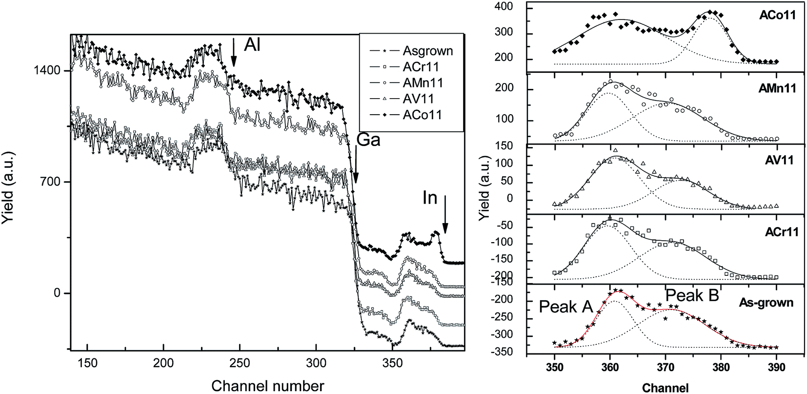 | ||
| Fig. 3 (left panel) RBS spectra for the as-grown and Cr, Mn, V, and Co ion-implanted AlInN/GaN layers, with an implantation dose of 5 × 1014 cm−2. Spectra are off-set along the Y-axis for the sake of comparison. (right panel) Indium part of the spectra. The data points and peak fitting are also shown. | ||
A negligible shift in the position of both peaks A and B is observed for Cr-, V- and Mn-implanted samples but the same effect is notable for the Co-implanted AlInN samples. The higher energy of backscattered alpha particles indicates the presence of target atoms near the surface. Therefore, the shift of the indium-related signal to a higher channel number indicates the migration of indium atoms towards the surface, which may be explained by assuming the interstitialcy interaction that was observed in the XRD results of the same samples.30 The high yield (less width) of the indium-related peak B and low yield (more width) of the indium-related peak A for the Co-implanted samples when compared to that of the as-grown samples indicates an upward shift of indium atoms. This likely happens due to the comparatively higher probability of the kick-out/interstitialcy process in the case of the relatively heavy ions of Co. A small diffusion of indium atoms towards the surface can be expected to produce a notable change in the relevant RBS signal because the indium content is already low in the currently used AlInN layers. The absence of any modification in Ga edge may rule out the possibility of the migration of the atoms of the host material and the penetration of implanted ions into the GaN layer. Moreover, the lack of any variation in the Al-related signal indicates the absence of any major change in Al distribution profile in the implanted samples.
Fig. 4 shows the RBS random spectra (and highlighted indium peak) of the ions implanted into the layers at a dose of 5 × 1015 cm−2. Similar to the RBS spectra measured for the samples implanted by the previous dose, the profile related to the Al and Ga edge remains unchanged after implantation at 5 × 1015 cm−2. The indium-related signal, however, shows considerable changes, especially for the cobalt-implanted samples. This indicates a decrease in the yield and area under the relevant curve, indicating a loss of indium atoms from the AlInN layer.
 | ||
| Fig. 4 (left panel) RBS spectra for the as-grown and Cr, Mn, V, Co ion-implanted AlInN/GaN layers, with an implantation dose of 5 × 1015 cm−2. The spectra are off-set along the Y-axis for the sake of comparison. (right panel) Indium part of the spectra. The data points and peak fitting are also shown. | ||
Fig. 5 presents the RBS random spectra as well as the separately highlighted indium peak for the samples implanted with the ions at a dose of 5 × 1016 cm−2. The results show modifications in the aluminum profile and Ga edge, indicating the redistribution of Al atoms and the penetration of implanted ions to GaN substrate. A notable loss of indium atoms is obvious for the Co-implanted samples. The spectra indicate the presence of implanted ions in the matrix, especially Mn and Cr for this highest implanted dose.
 | ||
| Fig. 5 (left panel) RBS spectra for the as-grown and Cr, Mn, V, Co ion-implanted AlInN/GaN layers, with an implantation dose of 5 × 1016 cm−2. The spectra are off-set along the Y-axis for the sake of comparison. (right panel) Indium part of the spectra. The data points and peak fitting are also shown. | ||
C. Magnetic properties
To investigate the prospects of ferromagnetism in the implanted samples, for realizing DMS materials, detailed magnetic temperature-dependent (MT) and magnetic field-dependent (MH) measurements were carried out. To characterize the magnetic materials, studies of the temperature dependence of magnetization are useful. The initial shape of the FC and ZFC curves, their bifurcation at different temperatures, and appearance of a cusp in ZFC curve provide valid signatures for identifying spin-glass, ferromagnetic, and superparamagnetic systems.31Thin films implanted with TM ions have often been reported to exhibit super-paramagnetism due to the presence of non-interacting single domain magnetic entities resulting from non-uniform dopant distribution.32,33 The FC, ZFC and MH curves provide important information to distinguish superparamagnetic and ferromagnetic materials. The observations of distinct FC and ZFC curves, an increase in magnetization in ZFC curves and a decrease in the magnetization of FC curves to trace the blocking temperature, availability of high saturation magnetization and zero remanence and zero coercivity are known features of superparamagnetic materials.34 The irreversibility between ZFC and FC curves and the appearance of a peak in the form of a cusp in ZFC curves are renowned signatures of spin-glass ordering, resulting from the frustration of spins in the matrix.35
Fig. 6 shows the MT curves and MH curves at 300 K for Cr, Mn, V, Co ion-implanted AlInN/GaN samples with a dose of 5 × 1014 cm−2. The absence of any upward tracking in FC and ZFC curves at the starting temperature, the weak difference between these curves at low temperatures and the negligible separation between these curves subsequently indicate the absence of notable ferromagnetism and possible paramagnetic features in AlInN samples implanted at the dose of 5 × 1014 cm−2 of Co ions. Moreover, the shape of the MH curve for this sample indicates a very weak hysteresis and a paramagnetic-like shape, especially at lower values of applied field. On the other hand, Cr-, Mn- and V-implanted samples demonstrate large bifurcation and upwards tracking of FC and ZFC curves at low temperatures in MT curves. Moreover, a clear hysteresis is observed in MH curves for these samples, which indicates ferromagnetism in these materials. The FC-ZFC separation is observed up to 160 K for Mn-implanted samples, 255 K for V-implanted and a considerably high measurable temperature of 350 K for the Cr-implanted AlInN samples. The MH curves support these observations, thereby indicating an increase in saturation magnetization in the same fashion. It is therefore concluded that AlInN samples implanted with Cr ions demonstrate a high temperature ferromagnetism (i.e., with a Curie temperature above 350 K) of significant magnitude when compared with other TM ions implanted at a dose of 5 × 1014 cm−2.
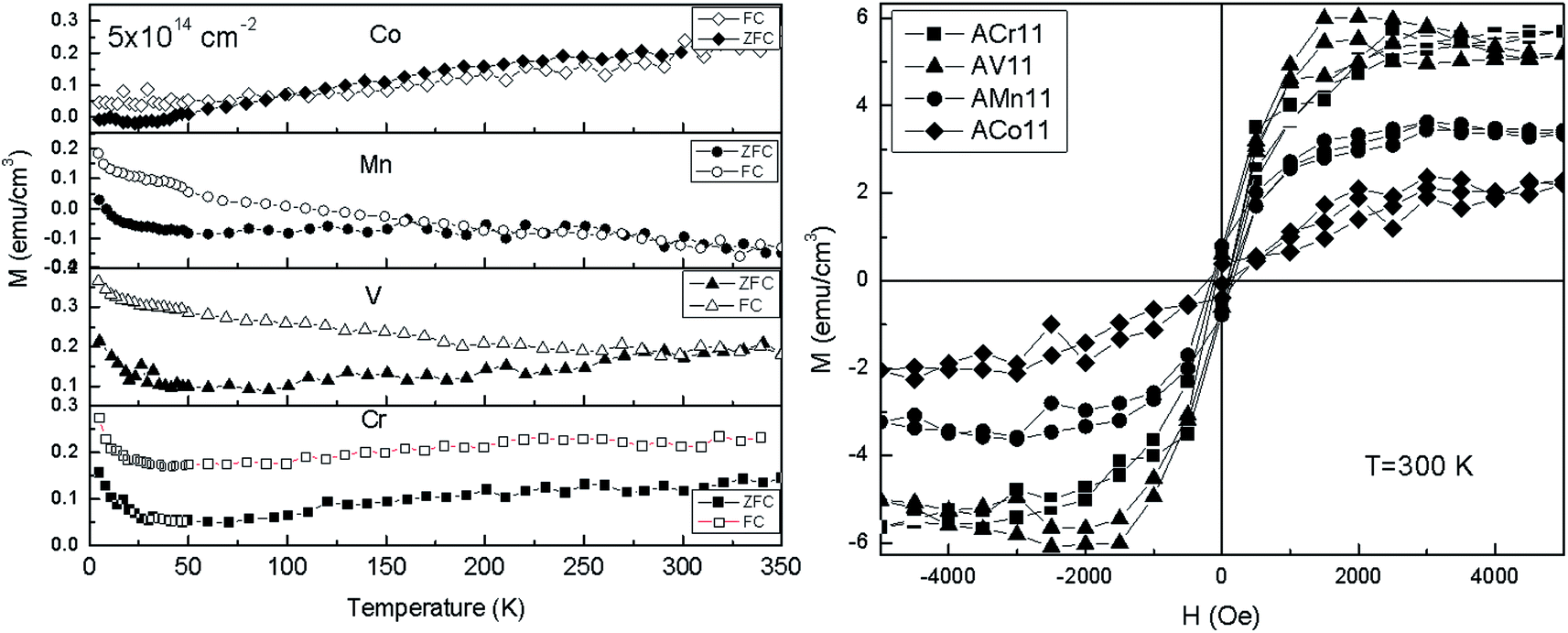 | ||
| Fig. 6 (left panel) MT curves showing FC and ZFC magnetization as a function of temperature and (right panel) MH curves at 300 K, for Cr, Mn, V, Co ion-implanted AlInN/GaN layers, with an implantation dose of 5 × 1014 cm−2. | ||
Fig. 7 shows MT curves and MH curves at 300 K recorded for Cr, Mn, V, Co ion-implanted AlInN/GaN layers at an implantation dose of 5 × 1015 cm−2. In the case of Mn:AlInN, although upward tracking at low temperature is available, the absence of difference between FC and ZFC throughout the measuring temperature and the weakest magnetic moment are observed from the MH curves, in comparison to other samples. This indicates a negligibly weak ferromagnetism in AlInN samples implanted with Mn ions at 5 × 1015 cm−2. The AlnN samples implanted with the dose of 5 × 1015 cm−2 Cr and Co exhibit FC–ZFC separation up to 225 K with nearly same and reasonably high value of magnetic moment. However, V-implanted AlInN samples bearing the same ion dose show that FC and ZFC are different above room temperature and exhibit the highest value of magnetic moment. Moreover, the shape of the MH curve for this sample indicates a very weak hysteresis and paramagnetic-like shape, especially at lower values of applied field.
 | ||
| Fig. 7 (left panel) MT curves showing FC and ZFC magnetization as a function of temperature and (right panel) MH curves at 300 K, for Cr, Mn, V, Co ion-implanted AlInN/GaN layers, with an implantation dose of 5 × 1015 cm−2. | ||
Fig. 8 shows the MT and MH curves at 300 K recorded for Cr, Mn, V, and Co ion-implanted AlInN/GaN layers at a dose of 5 × 1016 cm−2. All the samples exhibit a general trend of upwards tracking of FC and ZFC magnetization at low temperatures, which is a known gauge for ferromagnetism in magnetic thin films. For all the samples, the observation of hysteresis through the MH loops at temperatures higher than the blocking temperatures in the MT curves is consistent with the literature.36 In the case of Cr- and Co-implanted AlInN samples, the FC–ZFC difference ceases at 120 K, whereas a difference was observed up to the measuring temperature of 350 K, which indicates their potential as high-temperature diluted magnetic semiconductors.
 | ||
| Fig. 8 (left panel) MT curves showing FC and ZFC magnetization as a function of temperature and (right panel) MH curves at 300 K for Cr, Mn, V, Co ion-implanted AlInN/GaN layers with an implantation dose of 5 × 1016 cm−2. | ||
To produce a resourceful Mn:GaN-based DMS to exhibit carrier-mediated ferromagnetism, a Mn concentration of 5% is required.28 The observed ferromagnetism in the AlInN films at a TM dose of up to 5 × 1016 cm−2 (doping concentration of at.5%) could only be achieved via ion implantation that could introduce dopants, in the semiconductor matrix, above the solid solubility limits. It has been shown that Mn could be soluble up to 1% in GaN, after which secondary phases/clusters/precipitates are produced.37 Sofer et al. could attain 1% Mn concentration in their MOVPE-deposited GaMnN layers, which exhibited a small ferromagnetic component with the prevailing paramagnetic phase.38 Other studies in the literature include the synthesis of Ga1−xMnxN with Mn concentration of up to 0.6%,39 2%,40 1.33–3.2%,41 4%,42 and 2–5%.43 The attempts to obtain Ga1−xMnxN with a Mn concentration higher than 5% have barely been successful in producing homogenous DMS and have resulted in FM precipitates/clusters embedded into paramagnetic or anti-ferromagnetic structures.39–43
In the case of TM-doped nitride DMS materials, the hybridization between the sp of the valence orbitals and the TM 3d shells suggests prospects for carrier-mediated exchange interactions.44 However, ferromagnetism in TM ions implanted in DMSs is usually assigned to ferromagnetic secondary phases, clusters and precipitates, which rule out the possibility for carrier-mediated exchange interactions.45 This claim is supported by the commonly observed low carrier concentration of ion-implanted materials18 and the large exchange energy of TM dopants, which favor the formation of clusters.46 The observation of variable FC–ZFC characteristics and diverse room temperature MH features for the as-prepared AlInN samples implanted with different TM ions at different doses indicates ferromagnetic ordering in the materials. However, no dose-dependent and dopant-related consistency in the magnetic properties has been observed. This may not entirely be due to clustering, precipitation or the formation of secondary phases because the ion implantation and annealing conditions employed for this study introduced ions at different depths in the Gaussian profile. These considerations suggest the formation of simultaneous DMS alloy and TM-related phases/clusters/precipitates in the implanted samples. This explains the observation of inconsistent ferromagnetic features because spin ordering present in the materials may have emerged from both these coexisting ferromagnetic phases. Due to the low carrier density in ion-implanted materials and the formation of deep-gap states of the TM dopants in AlInN, the localized carriers or bound magnetic polarons are expected to foster exchange interactions in the materials.
4. Summary
A systematic computational and experimental analysis of TM-doped AlInN was carried out to explore the electronic, structural and magnetic properties of the materials. The DFT-based calculated results indicate that Mn introduces localized states and preferably occupies In sites in AlInN. The XRD results recorded for 5 × 1014 cm−2 TM ion-implanted AlInN/GaN indicated a shift of the AlInN-related peak to the lower angle side, which indicates an increase in the lattice constant of AlInN. The AlInN peak was, however, found to be absent for the samples implanted at 5 × 1015 cm−2 and 5 × 1016 cm−2, which suggests the structural degradation of the epilayers in the samples. The structural studies carried out using RBS indicate structural modifications and the migration of indium atoms across the interfaces of the structure. The MH and MT investigations conducted on the TM ion-implanted samples highlighted possible materials exhibiting high temperature ferromagnetic ordering suitable for spintronic applications. No doping-dependent consistency in magnetic properties was observed. The mechanism of the exchange interactions is expected to be due to the localized carriers or bound magnetic polarons in the materials.Acknowledgements
Prof. Dr Jianjun Zhu, Institute of semiconductor physics, Chinese academy of sciences, Beijing, China, is acknowledged for providing experimental facilities. Prof. Dr X. F. Han and Prof. Dr Rehana Sharif, Institute of Physics, Chinese Academy of Sciences, Beijing, helped in magnetic measurements.References
- M. Goorsky, Ion Implantation, InTech publisher, Croatia, 2012 Search PubMed.
- A. Meldrum, R. F. Haglund Jr, L. A. Boatner and C. W. White, Adv. Mater., 2001, 13, 1431–1444 CrossRef CAS.
- S. J. Pearton, C. R. Abernathy, G. T. Thaler, R. Frazier, F. Ren, A. F. Hebard, Y. D. Park, D. P. Norton, W. Tang, M. Stavola, J. M. Zavada and R. G. Wilson, Phys. B, 2003, 340–342, 39–47 CrossRef CAS PubMed.
- N. Gaur, S. N. Piramanayagam, S. L Maurer, R. W Nunes, S. Steen, H. Yang and C. S. Bhatia, J. Phys. D: Appl. Phys., 2011, 44, 365001 CrossRef.
- C. Choi, K. Noh, D. Choi, J. Khamwannah, C.-H. Liu, D. Hong, L.-H. Chen and S. Jin, IEEE Trans. Magn., 2012, 48, 3402–3405 CrossRef CAS.
- L. A. Larson, J. M. Williams and M. I. Current, Rev. Accl. Sci. Tech., 2011, 04, 11–40 CrossRef.
- O. Ambacher, J. Phys. D: Appl. Phys., 1998, 31, 2653–2710 CrossRef CAS.
- G. Liu, J. Zhang, X.-H. Li, G. S. Huang, T. Paskova, K. R. Evans, H. Zhao and N. Tansu, J. Cryst. Growth, 2012, 340, 66–73 CrossRef CAS PubMed.
- R. Butte, et al., J. Phys. D: Appl. Phys., 2007, 40, 6328 CrossRef CAS.
- J. C. Zolper, J. Cryst. Growth, 1997, 178, 157–167 CrossRef CAS.
- R. W. Martin, D. Rading, R. Kersting, E. Tallarek, E. Nogales, D. Amabile, K. Wang, V. Katchkanov, C. Trager-Cowan, K. P. O'Donnell, I. M. Watson, V. Matias, A. Vantomme, K. Lorenz and E. Alves, Phys. Status Solidi C, 2006, 3, 1927–1930 CrossRef CAS PubMed.
- K. Wang, R. W. Martin, E. Nogales, P. R. Edwards, K. P. O'Donnell, K. Lorenz, E. Alves and I. M. Watson, Appl. Phys. Lett., 2006, 89, 131912 CrossRef PubMed.
- A. Majid, G. Husnain, M. Usman, A. Shakoor, N. Hassan and J. J. Zhu, Phys. Lett. A, 2013, 377, 2986–2989 CrossRef CAS PubMed.
- A. Majid, A. Ali, J. J. Zhu and Y. T. Wang, J. Phys. D: Appl. Phys., 2008, 41, 115404 CrossRef.
- A. Majid, R. Sharif, A. Ali and J. J. Zhu, Jpn. J. Appl. Phys., 2009, 48, 040202 CrossRef.
- A. Majid, R. Sharif, A. Ali and J. J. Zhu, Appl. Phys. A, 2009, 96, 979–984 CrossRef CAS.
- N. Theodoropoulou, A. F. Hebard, S. N. G. Chu, M. E. Overberg, C. R. Abernathy, S. J. Pearton, R. G. Wilson and J. M. Zavada, Appl. Phys. Lett., 2002, 91, 7499 CAS.
- R. M. Frazier, G. T. Thaler, C. R. Abernathy, S. J. Pearton, M. L. Nakarmi, K. B. Nam, J. Y. Lin, H. X. Jiang, J. Kelly, R. Rairigh, A. F. Hebard, J. M. Zavada and R. G. Wilson, J. Appl. Phys., 2003, 94, 4956–4960 CrossRef CAS PubMed.
- Y. S. Cho, H. Hardtdegen, N. Kaluza, N. Thillosen, R. Steins, Z. Sofer and H. Lüth, Phys. Status Solidi C, 2006, 3, 1408–1411 CrossRef CAS PubMed.
- H. Hardtdegen, M. Hollfelder, R. Meyer, R. Carius, H. Munder, S. Frohnhoff, D. Szynka and H. Liith, J. Cryst. Growth, 1992, 124, 420–426 CrossRef CAS.
- H. Hardtdegen, M. Pristovsek, H. Menhal, J.-T. Zettler, W. Richter and D. Schmitz, J. Cryst. Growth, 1998, 195, 211–216 CrossRef CAS.
- J. F. Ziegler, J. P. Biersack, and U. Littmark, The Stopping and Ion Range of Ions in Solids, Pergamon, New York, 1985, vol. 1 Search PubMed.
- G. Te Velde, F. M. Bickelhaupt, E. J. Baerends, C. Fonseca Guerra, S. J. A. van Gisbergen, J. G. Snijders and T. Ziegler, J. Comput. Chem., 2001, 22, 931–967 CrossRef CAS PubMed.
- R. O. Jones and O. Gunnarsson, Rev. Mod. Phys., 1979, 61, 689–746 CrossRef.
- T. C. Schulthess, W. M. Temmerman, Z. Szotek, W. H. Butler and G. Malcolm Stocks, Nat. Mater., 2005, 4, 838–844 CrossRef CAS PubMed.
- T. Jungwirth, J. Sinova, J. Mašek, J. Kučera and A. H. MacDonald, Rev. Mod. Phys., 2006, 78, 809–864 CrossRef CAS.
- T. Graf, M. Gjukic, M. S. Brandt and M. Stutzmann, Appl. Phys. Lett., 2002, 81, 5159–5161 CrossRef CAS PubMed.
- T. Dietl, Nat. Mater., 2010, 9, 965–974 CrossRef CAS PubMed.
- V. A. Khonik, Metals, 2015, 5, 504–529 CrossRef PubMed.
- R. Rurali, P. Godignon, J. Rebollo, P. Ordejón and E. Hernández, Appl. Phys. Lett., 2002, 81, 2989–2991 CrossRef CAS PubMed.
- D. S. Williams, P. M. Shand, T. M. Pekarek, R. Skomski, V. Petkov and D. L. Leslie-Pelecky, Phys. Rev. B: Condens. Matter Mater. Phys., 2003, 68, 214404 CrossRef.
- H. P. Gunnlaugsson, T. E. Mølholt, R. Mantovan, H. Masenda, D. Naidoo, W. B. Dlamini, R. Sielemann, K. Bharuth-Ram, G. Weyer, K. Johnston, G. Langouche, S. Ólafsson, H. P. Gíslason, Y. Kobayashi and Y. Yoshida, Appl. Phys. Lett., 2010, 97, 142501–142503 CrossRef PubMed.
- D. H. Kim, J. S. Yang, Y. S. Kim, Y. J. Chang, T. W. Noh, S. D. Bu, Y.-W. Kim, Y. D. Park, S. J. Pearton and J.-H. Park, Ann. Phys., 2004, 13, 70–71 CrossRef CAS PubMed.
- A. F. Hebard, R. P. Rairigh, J. G. Kelly, S. J. Pearton, C. R. Abernathy, S. N. G. Chu and R. G. Wilson, J. Phys. D: Appl. Phys., 2004, 37, 511 CrossRef CAS.
- W. R. Chen, F. C. Zhang, J. Miao, B. Xu, X. L. Dong, L. X. Cao, X. G. Qiu, B. R. Zhao and P. Dai, Appl. Phys. Lett., 2005, 87, 042508 CrossRef PubMed.
- N. Theodoropoulou, A. F. Hebard, M. E. Overberg, C. R. Abernathy, S. J. Pearton, S. N. G. Chu and R. G. Wilson, Phys. Rev. Lett., 2003, 89, 107203 CrossRef.
- M. Zając, J. Gosk, E. Grzanka, S. Stelmakh, M. Palczewska, A. Wysmołek, K. Korona, M. Kamińska and A. Twardowski, J. Alloys Compd., 2008, 456, 324–338 CrossRef PubMed.
- Z. Sofer, D. Sedmidubský, J. Stejskal, J. Hejtmánek, M. Maryško, K. Jurek, M. Václavů, V. Havránek and A. Macková, J. Cryst. Growth, 2008, 310, 5025–5027 CrossRef CAS PubMed.
- I. T. Yoon, C. S. Park, H. J. Kim, Y. G. Kim, T. W. Kang, M. C. Jeong, M. H. Ham and J. M. Myoung, J. Appl. Phys., 2004, 95, 591–596 CrossRef CAS PubMed.
- M. H. Kane, S. Gupta, W. E. Fenwick, N. Li, E.-H. Park, M. Strassburg and I. T. Ferguson, Phys. Status Solidi A, 2007, 204, 61–71 CrossRef CAS PubMed.
- X. Cui and J. Zhang, Opt. Mater., 2015, 46, 299–303 CrossRef CAS PubMed.
- X. G. Cui, Z. K. Tao and R. Zhang, Appl. Phys. Lett., 2008, 92, 152116 CrossRef PubMed.
- M. Drygas, J. F. Janik, M. M. Bucko, J. Gosk and A. Twardowski, RSC Adv., 2015, 5, 37298–37313 RSC.
- K. Sato, et al., Rev. Mod. Phys., 2010, 82, 1633–1690 CrossRef CAS.
- S. J. Pearton, C. R. Abernathy, D. P. Norton, A. F. Hebard, Y. D. Park, L. A. Boatner and J. D. Budai, Mater. Sci. Eng., R, 2003, 40, 137–168 CrossRef.
- M. van Schilfgaarde and O. N. Mryasov, Phys. Rev. B: Condens. Matter Mater. Phys., 2001, 63, 233205 CrossRef.
| This journal is © The Royal Society of Chemistry 2015 |