Jabeen Fatima M. J,
Niveditha C. V and
Sindhu S*
Department of Nanoscience and Technology, University of Calicut, Thenhipalam, Kerala 673635, India
First published on 10th September 2015
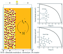
One of the many interfaces in Dye Sensitized Solar Cells (DSSC) which affects the performance of the cell is the photoanode–electrolyte interface. Material selection, its morphology, size and surface properties are found to control the electron transfer and transport behaviour of the photoanode. Here α-bismuth oxide (α-Bi2O3) is chosen as a photoanode material, which is synthesized by an easy and cost effective method, citrate nitrate gel combustion. Basic and specific analyses to study the properties of this material to use as a photoanode is done by using, X-ray diffraction (XRD), Scanning Electron Microscopy (SEM), UV-visible spectroscopy, Hall measurement and Electrochemical Impedance Spectroscopy (EIS). Since the electron transfer dynamics between photoanode–electrolyte interfaces have a significant impact on the performance efficiency of the cell, a detailed electrochemical impedance analysis is done by using bismuth oxide as the photoanode. Two different dyes, an organometallic dye (N719) and an organic dye (Eosin Y), are used as light harvesters in the cell structure with an iodine/iodide electrolyte. The performance efficiency of the photoanode is evaluated by recording the I–V characteristic of the cell under 1 sun illumination. The efficiency values obtained for dyes N719 and Eosin Y are 0.09 and 0.05% respectively and this is correlated with the impedance data obtained. Bode and Nyquist plots are used to explain the obtained results. Though nano bismuth oxide prepared by this synthetic method shows good charge carrier concentration, mobility and conductivity, the efficiency of the cell with the bismuth oxide photoanode is low. This low efficiency is attributed to the poor dye attachment and back recombination at the photoanode–electrolyte interface. Interface impedance data supports this argument and suggests modification of the oxide structure, morphology and surface properties for the improvement of efficiency.
Bismuth oxide is a semiconductor material with a wide bandgap ranging from 2.47 6 to 3.55 eV.7 The bandgap makes it an attractive material for various uses such as in photocatalysis,8 in sensor,9,10 supercapacitor11 etc. Bismuth oxide mainly exists in four major polymorphic forms namely α, β, γ and δ. The α form is stable at ambient condition; but δ form exists at high temperature only (i.e. above 730 °C) and there are rare reports of stable δ form at low temperature.12 The β and γ, polymorphs are metastable forms, which are stabilized by the addition of impurities or by controlling the reaction condition.13 Among four polymorphs the conductivity of β, γ and δ phases is ionic and that in α phase is electronic in nature.14 δ form is the most conductive polymorph with conductivity varying from 1 to 1.5 S cm−1.15,16 The n type nature of bismuth oxide is its positive aspect for photoanode application.
Various morphology of bismuth oxide has been reported by using different synthetic approaches like sol–gel,17 electrodeposition,18 flame pyrolysis,19 solvothermal,20 and thermal oxidation.21 Among these, the most common and simplest method of synthesis is sol–gel. For this reason, we opted for citrate–nitrate gel combustion method22 for synthesis of bismuth oxide nanoparticles. Basic and specific analyses required to study the properties of this material as a photoanode is done by using, X-ray diffraction, scanning electron microscopy, UV-visible spectroscopy, Hall measurements and electrochemical impedance analysis. Finally, the performance of the material as a photoanode is evaluated by applying this in DSSC.
The structural and phase identification of the prepared metal oxide is done by using X-ray diffraction analysis (XRD) with Rigaku miniplex X-ray diffractometer (Cu Kα – 0.15496 nm), scanned between 20–80°. The morphology of the synthesized bismuth oxide is done using SEM analysis (JEOL Model JSM 6390LV). The diffuse reflectance spectrum (DRS) is recorded by using JASCO UV-Vis spectrophotometer in the wavelength range 200 to 600 nm. The carrier mobility and conductivity are obtained from hall measurements (Ecopia HMS 5300). Electrochemical impedance, Mott–Schottky, and current–voltage behavior are measured using electrochemical workstation (Bio-logic SP150). Thin film of the semiconducting metal oxide coated on fluorine doped tin oxide glass plate is used for the electrochemical analysis with a three electrode system. Here the FTO substrate coated with bismuth oxide is used as working electrode, Ag/AgCl in saturated NaCl used as reference electrode and platinum wire as counter electrode. Electrolyte used is 0.1 M LiClO4. Photoanode was fabricated by doctor blade technique using scotch tape as spacer to maintain uniform thickness of the film in all cells fabricated for analysis. The paste for doctor blading is prepared by mixing metal oxide with Triton X 100 and isopropanol as solvent. The samples are then sintered at 400 °C for 30 minutes and used for dye loading. Two types of dyes, an organometallic dye namely N719 (di-tetrabutylammonium cis-bis(isothiocyanato)bis(2,2′-bipyridyl-4,4′-dicarboxylato) ruthenium(II)) and an organic dye, Eosin Y (2-(2,4,5,7-tetrabromo-6-oxido-3-oxo-3H-xanthen-9-yl)benzoate) are used for light harvesting. Both the dyes are purchased from Sigma Aldrich. The dye loading times are different for these two dyes and it is 30 minutes and 24 hours respectively for N719 and Eosin Y. An electrolyte mixture of 0.6 M 4-butyl methyl imidazolium iodide (BMII), 0.04 M iodine (I2), 0.1 M lithium iodide (LiI), 0.1 M guanidinium thiocyanate (GuSCN) and 0.5 M tertiary butyl pyridine in acetonitrile solvent is injected to the sealed cell with electrodeposited platinum as counter electrode. The I–V measurements are performed using AM1.5 Solar simulator (Scientech) under one sun illumination (100 mW cm−2). The radiation was calibrated with reference cell of monocrystalline silicon with sensitivity of ±5%. The impedance of the cells is measured under light and dark conditions.
The morphology of the synthesized metal oxide is analyzed using SEM. The sample showed irregular morphology with particles of varied sizes. Size determination is found to be difficult from the obtained image due to its agglomerated nature. SEM image is given in ESI as Fig. S1.†
The diffuse reflectance spectrum of the visibly yellow coloured metal oxide (Fig. S2 in ESI†) showed good absorbance with a wavelength ranging from 200 to 460 nm. The absorption wavelength of the dyes, used here as light absorbers (N-719 and Eosin Y), is around 500 nm, eliminating thus the chances of interference offered by the metal oxide for excitation. The energy gap between the Highest Occupied Molecular Orbital (HOMO) and the Lowest Unoccupied Molecular Orbital (LUMO) is determined using the bandgap obtained from the Tauc's plot for direct bandgap semiconductor.24,25
(αhν) = A(hν − Eg)1/2 | (1) |
Bismuth oxide is a direct bandgap semiconductor.26,27 Hence the Tauc plot is obtained by plotting (αhν)2 vs. hν, and a bandgap value of 2.70 eV is obtained from the graph (Fig. S3 in ESI†). The valence and conduction bandedge energy is calculated by using the eqn (2) and (3).28
EVB = χ − Ee + 1/2Eg | (2) |
ECB = EVB − Eg | (3) |
The photoluminescence (PL) study is done to determine the emission behaviour of the sample by exciting at the bandedge of absorption, i.e. at 416 nm. The major emission peak of bismuth oxide is seen at 466 nm and is attributed to the bandedge emission by the recombination of free excitons. Here, the photons are emitted as a result of the de-excitation of electron from the p level to the s level of bismuth ion.30,31 The bandgap is determined again from the PL spectrum by plotting PL intensity against energy (Fig. S5†). The obtained bandgap value is 2.70 eV and is well matched with the bandgap known from the Tauc plot.
Electrochemical impedance spectroscopy (EIS) is used to study the interface behavior of the metal oxide in the electrolyte (0.1 M LiClO4) medium. Here the impedance offered at the bismuth oxide–electrolyte interface is recorded from 1 MHz to 1 Hz under biasing from 0–1 V (Fig. 2a and b). When a semiconductor photoelectrode–electrolyte interface is created, Fermi level equilibration occurs between the systems by the transfer of electrons among them. Depending upon the position of the individual Fermi level, charge transfer takes place from semiconductor to electrolyte or vice versa until equilibrium attains. The impedance under this equilibrium condition gives the electrode–electrolyte interface impedance. Here, bismuth oxide semiconductor electrode and redox electrolyte interface impedance is measured by applying a potential externally, i.e. from 0.1 to 1 V. At a biasing potential of 0.1 V, the impedance of the system is found to increase due to the resistance offered by the initially acquired equilibrium at semiconductor–electrolyte interface. But on further increase of potential, from 0.1 V to 1 V, the resistance gradually decreases. On increasing the biasing potential to 0.2 V, a collapse of the previously acquired equilibrium occurs and that extends the Fermi level separation between the interfaces. After 0.2 V the impedance at the interface decreases as is visible from the Nyquist plot shown in Fig. 2a and b.
![]() | ||
Fig. 2 Impedance analyses of bismuth oxide in 0.1 M LiClO4 under different biasing voltages. (a and b) Nyquist plots. |
The impedance at the interface remains the same for a biasing of 0.3 V and 0.4 V, indicating the regaining of a new equilibrium. However, with a biasing range of 0.5 to 1 V a marked decrease can be seen in the measured interface impedance (Fig. 2b), signifying that the applied bias overcomes the Fermi level equilibration at the metal oxide–electrolyte interface.
The Bode plot of metal oxide–electrolyte interface gives peak at the same frequency under biasing but shows a change in phase. The corresponding Bode plot is shown in Fig. 3a and b. The peak maxima are obtained at a logarithmic frequency of 2.5 which corresponds to a frequency value of 316.23 Hz. The lifetime of electron residing on the conduction band of electrode is estimated from the equation.33
![]() | (4) |
The Nyquist and Bode plot at a range of biasing voltages from 0–1 V under 1 sun illumination is given in Fig. 4a and b. On illumination, the excitons are generated in the semiconductor, which helps in lowering the band bending. Further, when biasing is applied, the equilibrium collapses leading to a marked decrease in the impedance as represented in the Nyquist plot. This confirms the photoactive nature of the semiconductor metal oxide. The Bode plot of the sample under illumination shows shift in the frequency value compared to that in dark. The lifetime of electron calculated is varied from 5 to 2.5 ms with biasing from 0 to 1 V. The increased electron lifetime under illumination confirms the suitability of the material for photoelectrode applications.
In a semiconductor–redox electrolyte interface, equilibrium is attained as the electrons transfer from the valence band of the electrode to the redox system provided that the Fermi level of the semiconductor is above the redox potential of the electrolyte. The ensuing positive charge of the Fermi level of the semiconductor leads to band bending at the interface. Electrochemical impedance of this system under biasing leads to a situation where an applied potential does not create band bending and the system is said to be at flat band potential condition. At this condition, Mott–Schottky analysis which determines the depletion capacitance at the junction can be applied to find the built in bias at the metal oxide–electrolyte interface. The analysis is conducted in a three electrode system, with metal oxide coated FTO substrate as working electrode, platinum wire as counter electrode and Ag/AgCl in saturated NaCl as reference electrode. The electrolyte used is 0.1 M lithium perchlorate (LiClO4). The bias dependent depletion capacitance is related to the flat band potential and can be calculated using the equation34,35
![]() | (5) |
Fig. 5 depicts the Mott–Schottky plot of the metal oxide in 0.1 M LiClO4 by plotting C−2 versus bias voltage. In the plot, the capacitance at linear region represents the depletion capacitance. The flat band potential, donor density and type of majority charge carriers are estimated by fitting the above equation to the linear portion of C−2 versus bias voltage plot. The flat band potential calculated for bismuth oxide is −1.173 V with a donor density of 0.46 × 1021 cm−3 at 6.856 kHz frequency (ε of Bi2O3 is 37).36 Here the modulation frequency is judiciously selected by observing a linear response in the C−2 versus bias voltage plot. Frequency selection is important because the response of the charge carriers which contribute to the capacitance depends on the frequency of the applied signal. To ensure that all charge carriers contributed to the capacitance, low modulation frequency is to be applied for slow responding charge carriers and high frequency for fast responding carriers. The positive slope of the plot is explained by the n type conductivity in bismuth oxide system, which is in agreement with the Hall measurement results.
Performance of the bismuth oxide as photoanode is measured directly in DSSC and the current–voltage (I–V) behavior under 1 sun condition is recorded for a cell area of 0.25 cm2. Two different commercially available dyes, ruthenium based organometallic dye (N-719) and an organic dye (Eosin Y), are used as light harvesters with electrochemically deposited platinum as counter electrode and iodine/iodide redox couple in acetonitrile as electrolyte in DSSC. The I–V graph is depicted in Fig. 6. The efficiency of the sample is determined and the cell parameters obtained with both dyes are tabulated in Table 1.
Dye | Jsc (mA cm−2) | Voc (V) | FF (%) | η (%) |
---|---|---|---|---|
N719 | 0.243 | 0.68 | 52.6 | 0.09 |
Eosin Y | 0.197 | 0.50 | 52.3 | 0.05 |
The current–voltage characteristics of the cell under 1 sun illumination show the same fill factor values for both dyes. However, a comparative study shows that the efficiency of the cell with Eosin Y is lower than that with N719 dye. It is at once clear from the cell parameters that both the current density and open circuit voltage obtained with Eosin Y is lesser than that with N719. The bandedge alignment of bismuth oxide, N719 and Eosin Y shows that the LUMO of N719 is more negative than that of Eosin Y with respect to bismuth oxide conduction bandedge (Fig. S4 in ESI†). This indicate that the driving force for electron injection is higher in N719 than that in Eosin Y. Attempts are made to classify the reasons behind this low efficiency with Eosin Y, by analyzing the dye loading capacity and interface impedance of the cell while using these two dyes.
Dye loading is quantified from UV-Vis absorption spectrum by applying Beer–Lamberts law. According to Beer–Lamberts law the absorbance is directly proportional to the concentration of the solution. For a known concentration of sample the concentration of dye adsorbed on the photoanode is calculated. This is carried out by desorbing the dye from the metal oxide using 0.1 M sodium hydroxide solution. As a standard, 2 × 10⁻⁶ M solution of dye is prepared and tested for absorption, and then the concentration of the desorbed dyes N719 and Eosin Y are calculated and is found to be 6.54 × 10⁻⁷ mol L−1 and 1.157 × 10⁻⁷ mol L−1 respectively. The adsorbed concentration of Eosin Y is only 1/4 of N719, explaining the lowering of efficiency of the cell. However, the current due to Eosin Y is around 80% of that due to N719, this can be attributed to the high absorption coefficient of Eosin Y compared to N719. The UV-Vis absorption spectra of the two dyes are given as Fig. S6 in ESI.† Though bismuth oxide shows good charge carrier mobility and conductivity, its performance in a cell as a photoanode with N719 gives much lower Jsc and efficiency compared with that of TiO2 based photoanode.37 For bismuth oxide the nature of polymorph, its crystal structure, and nature of conductivity also influences the cell performance.2 Different surface properties of the polymorphs may affect the dye adsorption and electrolyte wetting property in DSSC and that influence the cell performance. Here with α-bismuth oxide the reduced dye adsorption, back recombination and the relatively less driving force for the transfer of photo-excited electrons from the dye to the metal oxide may explain the poor performance of the cell. The flat band potential value calculated from Mott–Schottky plot for bismuth oxide is relatively negative, hinting at the reduced driving force for photoelectron transfer.
A detailed interfacial impedance analysis of dye sensitized solar cells is done using electrochemical impedance spectroscopy by plotting Nyquist and Bode plot. The four major interfaces that are identified in a DSSC are (i) FTO–metal oxide, (ii) counter electrode–electrolyte, (iii) metal oxide–electrolyte and (iv) Warburg diffusion of the ions in the electrolyte. The Nyquist plot of the cell, given in Fig. 7, is labeled with 3 characteristic frequencies ω1, ω2, and ω3, corresponding to three major interfaces respectively, the counter electrode–electrolyte interface, semiconductor–electrolyte interface and ionic diffusion occurring in the electrolyte.
Nyquist plots for cells with N719 and Eosin Y are recorded at an open circuit condition under illumination (Fig. 7) with three major semicircles. The values obtained were fitted according to the equivalent circuit given in ESI as Fig. S7,† where the impedance offered by the FTO–metal oxide interface is denoted as Rs.
The first semicircle denotes the impedance offered by the counter electrode–electrolyte, i.e. the platinum–iodine iodide interfacial impedance. This has a parallel combination of resistance and capacitive elements which are denoted as R1 and C1. The second semicircle represents semiconductor–electrolyte interface with resistive and capacitive elements R2 and C2 in the equivalent circuit. Final semicircle denotes the impedance offered by diffusion of the ions in the electrolyte (Warburg impedance). The diffusion resistance also appears as series combination of resistance and capacitance denoted as R3 and C3. The cell parameters are determined from the curve given in Fig. 7 and are tabulated in Table 2.
Dye | Rs (Ω) | R1 (Ω) | C1 (F) | R2 (Ω) | C2 (F) | R3 (Ω) | C3 (F) |
---|---|---|---|---|---|---|---|
N-719 | 15.08 | 5.07 | 13.87 | 39.41 | 168.11 | 40.72 | 2832.00 |
Eosin Y | 10.93 | 4.07 | 8.78 | 30.16 | 64.19 | 55.83 | 5608.89 |
Interface impedance of the cells with dyes N719 and Eosin Y shows comparable series resistance (Rs). R1 and C1 values are relative and found to be slightly higher for the cell with N719 than that with Eosin Y. R2 and C2 value obtained for N719 is slightly higher than that obtained with Eosin Y. The metal oxide–electrolyte interface impedance influences the recombination possibilities of the charge carriers from the bismuth oxide conduction band to the redox electrolyte. While comparing the data obtained for the cells with N719 and Eosin Y, the recombination possibilities will be higher in the cell with Eosin Y, as R2 and C2 are smaller to that obtained with N719. This can be correlated with the efficiency of the cell obtained with these two dyes along with the dye adsorption behavior. However, no considerable difference in the resistance values is observed in the present experiments and the offered resistance is not very high also. A high recombination rate at the metal oxide–electrolyte interface is there by made possible leading to lowered current density. The R3 component indicates the resistance offered by the ionic movement in the electrolyte. The values obtained are 40 and 55 Ω respectively for N719 and Eosin Y sensitized solar cells. One of the major factors determining the ionic resistance is the distance between the two electrodes. Even though the fabrication procedure and the sealant material used are the same, manual errors may cause slight changes in the cells. The high R3 and C3 values given by Eosin Y sensitized cell again correlates with its relatively poor performance.
Fig. 8 depicts the Bode plot of DSSC with dyes N719 and Eosin Y. Bode plot can be represented as phase versus frequency/log frequency or log|Z| versus frequency/log frequency. The counter electrode–electrolyte interface appears to fall in the frequency range of 105 to 103 Hz.3,4 The semiconductor–electrolyte interfacial impedance falls in the frequency range of 103 to 102 Hz. The Warburg diffusion impedance is seen at lower frequencies, at around 101 Hz.38 Here, the frequency range of 103 to 102 Hz is focused for the calculation of lifetime of electron in the semiconductor conduction band by using the equation previously mentioned. The frequency maximum obtained for N719 sensitized cell is 218 Hz and the calculated lifetime of electrons in the photoanode is 0.7 ms. For Eosin Y sensitized cell, the frequency maximum is seen at 370 Hz and the calculated electron lifetime is 0.4 ms.33 The charge transfer resistance at the electrode–electrolyte interface obtained for the cells with N719 and Eosin Y are proportionate to the calculated life time of electrons in the metal oxide photoanode. Relatively large charge transfer resistance and longer lifetime observed for the cell with N719 indicates the reduced charge recombination possibilities at the electrode–electrolyte interface. This back recombination rate of electron from the oxide conduction band to the redox electrolyte affects the open circuit voltage also. A comparison of the I–V parameters of these two cells shows that the comparatively low efficiency given by Eosin Y sensitized cell is mainly due to low open circuit voltage. The low adsorbed concentration of Eosin Y in the metal oxide results in increased electrode–electrolyte interfaces and encourages the back recombination of electrons. One of the reasons for different dye loading percentage on the same photoanode material can be attributed to the structural changes in the dyes used.
Footnote |
† Electronic supplementary information (ESI) available. See DOI: 10.1039/c5ra12760b |
This journal is © The Royal Society of Chemistry 2015 |