
Formation of high-quality perovskite thin film for planar heterojunction solar cells†
Shuang Yang,
Ying Chen,
Yi Chu Zheng,
Xiao Chen,
Yu Hou and
Hua Gui Yang*
Key Laboratory for Ultrafine Materials of Ministry of Education, School of Materials Science and Engineering, East China University of Science and Technology, 130 Meilong Road, Shanghai 200237, China. E-mail: hgyang@ecust.edu.cn
First published on 7th August 2015
Abstract
Constructing uniform, flat perovskite thin films is of paramount essence to achieve high performance and reproducible perovskite photovoltaic devices. However, the sequential deposition technique, which usually shows efficiencies over 17%, still failed to enable the formation of uniform, pinhole-free films by solution processing, whereas such high-quality films can be prepared within the vapor medium. Here we demonstrate that such high-quality film can also be realized upon a solution process via judicious choice of solvents, particularly by controlling of lead dissolution phenomenon. We found that alcohol solvents with appropriate molecular structures such as tert-butanol, can facilitate the in situ intercalation of ammonium cations into PbI2 matrix, and thus give flat mirror-like tetragonal perovskite film with resemble surface roughness to that from vapor assisted method. Planar heterojunction solar cells constructed with these solution-processed thin films yielded a high power conversion efficiency of 14.61%, extremely higher than that of conventional method under standard one sun conditions. This solvent-mediated strategy provides a new approach towards the goal of high-performance, low-cost and reproducible devices with simple solution processes.
Introduction
As both a conventional and current technique, solution processed thin film photovoltaics has been widely studied for decades due to its promise for the realization of low-cost, large-area, flexible and portable devices. Recently, the perovskites solar cells (PSCs) employing organolead halide perovskite CH3NH3PbX3 (X = Br, I) absorbers emerged with an astonishing efficiency over 20% within only five years.1,2 For a typical PSC, hundred nanometer-thick perovskite absorber and window material films are closely stacked between conductive substrate and back contact.3–6 This emphasizes the significance of developing perovskite films with constant thickness and flat surface in a large area. Unfortunately, during the solution-processed fabrication, thin perovskite film usually presents a rough surface which integrates large pinholes and metal/semiconductor/metal-like regions into the devices and further compromises the power convention efficiency by causing high leakage currents.7–9To avoid the shunting phenomenon in these devices, mesoporous TiO2 or Al2O3 scaffolds were firstly incorporated by the infiltration of perovskite precursors.10,11 But the drawback is that the scaffold does not show means for the final energy conversion efficiency and thus the planar devices would be more attractive in the future.12,13 This can be achieved via a sequential deposition route by reacting predeposited uniform PbI2 film with CH3NH3I isopropanol (IPA) solution or gaseous molecules.14–17 However, when conducted in the liquid medium, PbI2 is partially dissociated and recrystallized into fluctuated morphologies of cubed-shaped perovskite crystals at hundred nanometer scale, which has a rather detrimental effect on photovoltaic performance.18 Alternatively, the sequential reaction in the vapor or vacuum media is dominated by the in situ intercalation of methylammonium iodide that PbI2 crystals gradually expand with reduced interspace between each particle whose final surface roughness usually keep parallel to the pristine PbI2 films.8,19,20 In principle, this dissociation behavior is highly dependent on the solvent effect in the solution process and thus, we have been motivated to make a judicious selection of solvent that enables the formation of uniform, pinhole-free perovskite films upon the in situ crystallization mechanism.
In this report, we have carefully studied the contribution of various solvents for the lead dissolution behavior based on the sequential reaction of large PbI2 crystals, and found the alcohol solvents with branched structures, such as tert-butanol (TBA), can facilitate the CH3NH3I in situ intercalation into PbI2 matrix efficiently. It was also found that the PbI2 film in such liquid media gradually expanded with the CH3NH3I intercalation and thus, giving mirror-like films with the similar roughness to that from the vapor assisted route. Overall, photovoltaic devices exemplified here show significant improvement in power conversion efficiency, compared with that of conventional sequential reaction method.
Experimental section
Materials synthesis
Lead iodide crystals were synthesized by a modified method according to the literature.25 Typically, 0.0971 g lead nitrate (Pb(NO3)2, 99%, Aldrich) and 0.01 g cetyltrimethylammonium bromide (CTAB, 99%, Aldrich) were dissolved in 25 mL deionized water. Then 5 mL of 0.06 M potassium iodide (KI, 99%, Aldrich) aqueous solution which acted as iodine precursor was slowly dropped into the Pb(NO3)2 solution under vigorous stirring at 700 rpm, and a yellow coloured precursor was obtained. The mixture of 30 mL was transferred into a Teflon-lined autoclave and treated at 120 °C for 36 h in an oven. After cooled to room temperature, the solid products obtained were raised with H2O twice (15 mL each time), dried at 60 °C overnight in a vacuum oven.CH3NH3I was synthesized by a solution reaction of 24 mL methylamine solution (33 wt% in ethanol, Aldrich), 10 mL hydroiodic acid (HI, 57 wt%, Aldrich) and 100 mL ethanol (99.7%, Shanghai Lingfeng Chemical reagent) in 250 mL round bottomed flask under nitrogen atmosphere at 0 °C for 2 h under stirring. The precipitate was recovered by evaporation at 50 °C for 2 h, washed with diethyl ether three times and finally dried at 60 °C in vacuum oven overnight.
The followed sequential reaction was conducted by different solvents at room temperature according to our previous report.14 In a typical synthesis, 10 mg of PbI2 was firstly added in 5 mL isopropanol (IPA, 99.7%, Aldrich). These PbI2 crystals can not be dissolved and to ensure well dispersion, the obtained suspension was further treated in ultrasonic bath for 5 min. Then 5 mL of 20 mg mL−1 CH3NH3I isopropanol solution was dropwise added into the PbI2 suspension under magnetic stirring. The colour of the precipitates changed from yellow to dark brown and finally to black. After stirring for 2 h, the products were separated by centrifugation, washed three times with hexane or chlorobenzene and finally dried at 60 °C for 2 h in a vacuum oven.
Device fabrication
FTO glass substrates (Nippon Sheet Glass, Japan, 8 Oper square) were firstly patterned by etching with Zn powder and 2 M HCl diluted in deionized water. Then cleaned by ultrasonication with soap, acetone, deionized water, and ethanol. To make a compact layer of TiO2, the FTO glasses were coated with mildly acidic solution of titanium isopropoxide in ethanol by the spin-coating method at 3000 rpm for 30 s, followed by a thermal treatment at 500 °C for 30 min. The PbI2 film was prepared by spin-coating 1 M PbI2 (99.9985%, Alfa Aesar)/N,N-dimethylformamide (DMF, 99.9%, Alfa Aesar) solution at 3000 rpm for 15 s and then was kept at 100 °C for 5 min. After cooling to room temperature, 150 μL of 6 mg mL−1 CH3NH3I solution in isopropanol or tert-butanol were loaded on the PbI2-coated film for 40 s followed by spun at 4000 rpm for 20 s and annealed at 100 °C for 5 min. Before spin-coating of the tert-butanol solution, the substrate and CH3NH3I solution were held at 60 °C for 2 minutes. Hole conductor material (HTM) was deposited by spin-coating at 4000 rpm for 30 s. The spin-coating formulation was prepared by dissolving 72.3 mg spiro-MeOTAD, 18 μL of a stock solution of 500 mg mL−1 lithium bis(trifluoromethylsulphonyl)imide in acetonitrile and 29 μL 4-tert-butylpyridine in 1 mL chlorobenzene. Finally, silver was thermally evaporated onto the HTM layer as the back contact. The devices were left in a desiccator overnight before tested. All the device fabrication process were carried out in an Ar-filled glove box.Characterization
Crystallographic information of the as-synthesized crystals was investigated by powder X-ray diffraction (XRD, Bruker D8 Advanced Diffractometer, Cu Kα radiation, 40 kV). The morphology and structure of the samples were characterized by field emission scanning electron microscopy (FESEM, HITACHI S4800). The Pb content dissolved in solution was determined by inductively coupled plasma atomic emission spectroscopy (ICP-AES). The optical absorption spectra were measured by using a Cary 500 Spectrophotometer. The current–voltage tests of solar cells were performed using a solar light simulator (Oriel, 91160, AM 1.5 globe) and the power of the simulated light was calibrated to 100 mW cm−2 using a Newport Oriel PV reference cell system (model 91150 V). All cells were measured using a Keithley 2400 source meter. Devices were masked with a metal aperture to define the active area of 0.0625 cm−2.Results and discussion
For the sequential deposited devices, the occurrence of irregular fluctuations on the film surfaces are mainly because of the intrinsic dissolution of lead framework and subsequent recrystallization into the cube shaped perovskite crystals (Fig. 1). But concerning the large PbI2 interlayer space of 2.66 Å,21 the in situ intercalation of ammonium cations should also be another route to produce tetragonal perovskite crystals. This indicates that uniform perovskite film is also accessible by using appropriate liquid medium, in a process which is dominated by in situ intercalation. The key factor for the formation of high-quality perovskite film lies in the suppression of lead dissolution and thus, the corresponding dissolution behaviour must be systematically studied in different liquid media. | ||
| Fig. 1 Schematic of formation mechanisms of perovskite films by using TBA as solvent via the sequential reaction route. In contrast to the common solvent, typically IPA, the dissolution–crystallization phenomenon can be significantly suppressed in such liquid media, whereas the in situ intercalation plays the dominate role. | ||
To provide a clear, visual distinction upon the solvent effects, we associate them with the sequential reactions based on micron-sized hexagonal PbI2 crystals (Fig. S1†). Such material enables both readily observability and minimum surface area stemmed from its flat surface and large crystal size. Because in situ intercalation normally initiates form the surface toward the inner spaces,22 its role is believed to be negligible when small surface area is available on these large crystals. Here, we sought to compare six solvents, including 1-propanol (PA), 1-butanol (BA), 1-hexanol (HA), IPA, TBA and tert-pentanol (TPA), and their 3D molecular structures are presented in the insets of Fig. 2A. All PbI2 crystals were reacted with CH3NH3I solution under ambient temperature for 15 min. In contrast to the pristine regular PbI2 crystals, scanning electron microscope (SEM) images revel that all the microcrystals are kept their hexagonal geometries but with distinctive, hierarchical surface motifs (Fig. 1A). Closer inspection of the surface of these crystals (Fig. S2†) shows cube shaped crystals which are expected for the tetragonal CH3NH3PbI3 crystallographic phase, and more importantly, the particle size which varied from micron- to nano-scales, is highly dependent on the molecule structure of corresponding solvents. This emphasizes the important role of solvents in the dissolution–recrystallization process as observed. Interestingly, the recrystallization phenomenon frequently occurred with ordered arrangements which may be preferentially along specific lattice orientations, such as [001].23 Away from the identical atomic arrangement of PbI2, another possible reason is the orient attachment of dissociated perovskite crystals onto the parent surface. For the film assembled with the cube shaped particles, it generally displays many large spatial vacancies, which will give rise to a host of shunt pathways and poor light-to-electricity response in photovoltaic devices.
 | ||
| Fig. 2 (A) SEM images of the products after the sequential reaction for 10 min with different solvents. Cube shaped particles on the surface are CH3NH3PbI3 crystals derived from the dissolution–recrystallization process. Insets are the corresponding 3D molecular structures of the solvents used. Scale bars are 5 μm. (B) Dependence of the CH3NH3PbI3 perovskite particle size on the solvents extract form the SEM images. Error bars for (B) represent one standard deviation of the measured sample distribution (minimum 100 particles). (C) Relationship between the dissolved Pb concentration (left axis) and ratio (right axis) versus different solvents after the sequential reaction. (D) XRD patterns of the products synthesized with different solvents. The red and black labels account for PbI2 and CH3NH3PbI3 crystalline structure, respectively. (E) CH3NH3PbI3 perovskite conversion ratio calculated from the corresponding XRD patterns in (D). | ||
In situ intercalation is typically believed to be a layer by layer intercalation of ammonium cations, and regarding the low accessible surface area of these large PbI2 crystals, dissolution–recrystallization should play the dominate role in this process. Therefore, the size of the surface cube shaped crystals can partly reflect the extent of dissolution–recrystallization behaviours in various solvents. The average size of the samples are shown in Fig. 1B and S3.† As the chain length become longer from PA to HA, there was an obvious reduction of the formed cube crystals, which indicates the long chain length of solvents is not favorable for the dissolution–recrystallization process. Low polarity of the solvents may have a negative effect on the lead dissolution and moreover, high viscosity is likely to retard the diffusion of the solutes.
It can be clearly observed that the smaller solvent molecular favors the dissolution of PbI2. It can be clearly observed that the smaller solvent molecular favors the dissolution of PbI2, however, despite the identical chemical components of PA and IPA, IPA generated a much smaller mean size about one third of the PA samples. Based on their physical properties, one can conclude that the predominant parameter should lie in molecular polarity: the empirical parameter of solvent polarity (ET value) for PA and IPA are indexed to be 0.617 and 0.546 (1 for H2O), respectively. Complementary to the morphological results, the dissociated Pb content in the residual solvents from a sequential reaction can be rationalized by inductively coupled plasma atomic emission spectroscopy (ICP-AES). The values of dissolved Pb content included in Fig. 1C demonstrated a similar sequence in comparison with the trend of the perovskite crystal size. It is worth mentioning that even with more Pb dissolved in HA, its crystal size was still less than the TBA sample. The major difference between HA and TBA is the presence of long chain length, which may be unfavourable for the diffusion of solute during the recrystallization process.
X-ray diffraction (XRD) patterns of the products show that all samples can not be well transformed into the perovskite phase, and thus the hexagonal PbI2 lattice is still enriched in the center of the particles (Fig. 1D). We then employed a standard PbI2/CH3NH3PbI3 sample to give a quantitative analysis of the perovskite weight ratio. The relative intensity ratio (K) can be expressed as following equation,
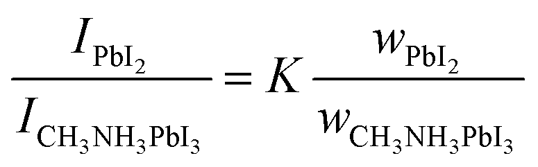 | (1) |
A K value of 2.561 was calculated by the intensities of PbI2 (110) and CH3NH3PbI3 (101) peaks. The obtained weight ratio was then translated into the reaction ratio of PbI2 as shown in Fig. 2E. It is rather surprising that there is an obvious mismatch with the above results: solvent molecules with branched chain structures (IPA, TBA and TPA) generated considerable higher conversion ratio, and particularly these values should be underestimated because of the more Pb loss during the intensive dissolution in other solvents. But it is not surprising when concerning the polarity of the solvents with branched structures reduce significantly with ET values of 0.389 and 0.321 for TBA and TPA. It has been known that the weak polar or non-polar solvents can thermodynamically facilitate the formation of perovskites which act as the anti-solvents. Alternatively, in weak polar solvents, ammonium cations is expected to react with the lead framework in another manner, that is, the in situ crystallization mechanism. Therefore, the presence of the in situ crystallized perovskites should locally cause the mismatch between the depth of surface cubed shaped crystals and calculated phase conversion values.
Based on above results, we concluded that a suitable solvent must meet two standards, high phase conversion ratio as well as slow dissolution–recrystallization rate compared with the commonly used IPA. We then selected TBA as the solvent which can meet both demands to deposit CH3NH3PbI3 films. The procedure in this work was on the basis of the Park's method which involves initial preparation of PbI2 films and sequential spin-coating of CH3NH3I solution. All perovskite films were fabricated on planar TiO2 compact layers without mesoporous layers. Fig. 3A shows the XRD patterns of the CH3NH3PbI3 perovskite films by using TBA and IPA as solvents. Diffraction peaks at 12.67° can be assigned to lattice planes of hexagonal 2H PbI2 polytype (space group: P3m1(164), JCPDS file No. 07-0235), which implies the existence of trace amount of unreacted PbI2 in both samples. Most intriguingly, TBA as the solvent generated a mirror-like perovskite film that even the inverted background of letters could be clearly seen (inset in Fig. 3B). The UV-vis absorption spectra of TBA and IPA samples appears to have similar light absorption capacity with almost identical amount of CH3NH3PbI3 loaded on the substrate (Fig. 3B). The slightly lower absorption of IPA film should be regarded as the loss of lead upon its fast dissolution.
 | ||
| Fig. 3 (A) XRD patterns of the perovskite films prepared with different solvents and the bare TiO2/FTO substrate. The red and black labels correspond to PbI2 and CH3NH3PbI3 phase, respectively. (B) UV-vis absorption spectra of the as-prepared perovskite films. The inset is the digital photograph of IPA and TBA films. SEM and AFM images of perovskite films formed in different liquid media: (C) IPA and (D) IPA. Insets in the AFM images are the height profiles of the green lines in the figures. Scale bars for the left and the right of the two figures are 2 μm and 500 nm, respectively. | ||
Fig. 3C and D show the surface characteristics of IPA and TBA films. As expected, both perovskite films allowed the almost full coverage of the substrates, but many hundred nanometer holes can be observed on the IPA film, which is correlated with its dissolution of lead framework. Moreover, the following anisotropic growth of perovskites must be happened along the remained ones, which reversely broaden the native holes on the PbI2 films. By contrast, the TBA film is found to be much more flat and uniform with the slight nanosized holes. We also used atomic force microscopy (AFM) imaging to evaluate the surface morphological characteristics. For the pristine PbI2 film, the surface roughness values of the arithmetic average (Ra) and the root mean square (Rq) are 9.47 and 12.10 nm for the whole scanned area. After the sequential reaction in IPA, the sub-microscale crystals formed with heights ranging from −300 to 300 nm, showing the much enhanced Ra and Rq value of 74.2 and 54.8 nm, respectively. Nevertheless, film stemmed from TBA exhibits the Ra and Rq values of 17.9 and 14.1 nm, which is even comparable to the vapor-assisted films.8,19 In view of the similar grain size of the TBA and PbI2 films (Fig. S5 and S6†), we believe that the dissolution–recrystallization should be considerably suppressed in TBA during the sequential reaction.
To shed light on the formation mechanism of the uniform perovskite film, their growth process was monitored by spun the CH3NH3I TBA solution at different intervals of reaction time (Fig. 4A). All films exemplified here were reacted with 6 mg mL−1 CH3NH3I TBA solution and subsequently heated at 70 °C for 10 min. The pristine PbI2 film shows uniform sheet-like shapes with a few scattered voids among adjacent grains. Interesting, when the reaction time at 5 s, the entire crystal geometries were remained, but their irregular surfaces evolved into flat facets. This is probably because the introduction of liquid/solid interface could trigger the fast surface dissociation of PbI2, and then exposure the thermodynamically favorable facets. From 15 s to 40 s, the crystals gradually turned to polyhedrons and expanded to a much larger cell volume (4.557 × 4.557 × 6.979 for PbI2, 8.855 × 8.855 × 12.659 for CH3NH3PbI3) with the diminish of large voids among adjacent grains. Noteworthily, the interstitial voids in IPA and TBA present the opposite growth trend, which may be explained as the different crystallization mechanisms. Further reacting with CH3NH3I for 60 s, triangular pyramid shaped crystals were generated on the surface which indicates the occurrence of dissolution–recrystallization. The film colour varied from light brown to dark black with about 30 s, which is relatively slow than the reported values. Park et al. have investigated the geometrical variation as a function of the loading time by using IPA as solvent and found that small cube shaped nucleus were firstly formed locally onto PbI2 surface with an similar CH3NH3I concentration.14 However, reviewing the whole process in TBA, no apparent perovskite nucleus or changes in crystal size can be found and thus, we believe this slow phase transformation is dominated by an in situ crystallization process.
 | ||
| Fig. 4 (A) Surface SEM images of the films with different CH3NH3I loading times. All scale bars are 500 nm. (B) Schematic illustration of the sequential reaction process by using TBA and IPA as solvents for fabricating perovskite films. | ||
Based on above results, we can concluded that the use of TBA can offer multiple merits: the first is the low dissolved rate of lead which can suppress the formation of cube shaped perovskite crystals with numerous large pinholes (Fig. 4B); the second is that reduced lead is lost during the reaction process; the third is that the gradual expansion of crystals in the in situ crystallization process can reversely eliminate the voids between each crystals. After 100 °C annealing, the grains contact more closely but a small amount of nanosized holes still existed. We anticipate holes at this scale would not cause the leakage current in a device. A higher CH3NH3I concentration of 10 mg mL−1 was also attempted that some cuboid shaped crystal emerged onto the surface (Fig. S7†). This is consistent with the results by using longer reaction time that the dissolution–recrystallization gradually make a more pronounced sense.
Solar cells were fabricated with a planar heterojunction configuration as shown in Fig. 5A. The photocurrent density–photovoltage (J–V) curves of typical solar cells stemmed from different solvents were measured under irradiation with air mass (AM)-1.5 global simulated sunlight at an intensity of 100 mW cm−2 (Fig. 5B). All scans were taken from forward bias to short circuit with a scan rate of 0.15 V s−1. The perovskite device based on TBA film yields a higher Voc (965 mV), short-circuit current density Jsc (19.3 mA cm−2), and fill factor FF (66.2%) than the device based on pristine IPA film (Voc = 890 mV; Jsc = 17.1 mA cm−2; FF = 54.9%). The device based on TBA had power conversion efficiency (PCE) = 12.32%, whereas the device based on pristine IPA had PCE = 8.35%. To further verify the reliability of above J–V results, the device was held at a forward bias of 0.69 V as a function of time to monitor the stabilized power output (Fig. 5C). The photocurrent stabilizes within seconds to approximately 17.4 mA cm−2, yielding a stabilized PCE of 12.0%, measured after 600 s. The hysteresis behaviour of this device was also measured that the forward scan delivered slightly lower PCE value (11.13%) than that of the reverse scan (12.32%) under a scan rate of 0.15 V s−1 (Fig. S8†). Noteworthily, the J–V characteristics of the champion TBA device have attained a Jsc of 20.9 mA cm−2, a Voc of 993 mV and a FF of 0.73, yielding a PCE of 14.61% (Fig. S9†).
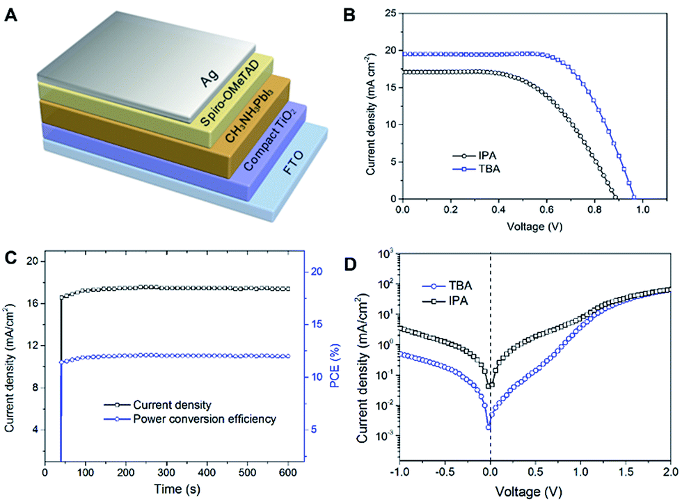 | ||
| Fig. 5 (A) Schematic illustration of a typical planar photovoltaic device. (B) J–V curves under AM 1.5 simulated illumination and (C) logarithmic plots of dark J–V characteristics of PSCs based on IPA and TBA films. (D) Photocurrent density and PCE as a function of time for the TBA device held at a forward bias of 0.69 V. The cell was placed in the dark prior to the start of the measurement. | ||
Due to the similar light absorption capacities of both films, this shortfall of Voc, Jsc and FF should be ascribed to the high leakage current in the IPA device. Fig. 5D shows dark current densities of these devices. The IPA device exhibits a huge leakage current density larger than 1 mA cm2 even under a reverse bias of 0.5 V. In comparison, the dark current of TBA device is dramatically reduced over one orders of magnitude, suggesting that the occurrence of shunt pathways as a result of the surface morphological fluctuations of perovskites films. It has been known that the origin of shunt currents in thin film devices can be classified into three types: (1) ohmic shunts of pinholes across the absorber layer; (2) space charge limited currents between the front/back contact and absorber semiconductor region and (3) the tunnelling currents via high densities of mid-gap defect states.7,9,24 We therefore investigated SEM cross-sectional profile of the TBA films after coating of spiro-OMeTAD layer to visualize the surface leakage pathways (Fig. S9†). Clearly, the high salient sites would directly joint to the back contact even with a relative thick hole conductor layer. This is consistent with the J–V results in reverse-bias which presents a non-ohmic shunt characteristics with the voltage range of 1 V (Fig. S10†). Moreover, sub-micron voids across the entire absorber layer which act as pinholes still remained owning to the large surface basins. On the basis of these results, one can reasonably deduced that the in situ crystallization approach can significantly suppress the leakage currents from the surface non-uniformity of perovskite layer and thus, yields more reproducible and efficient devices.
Conclusions
In conclusion, we have demonstrated that the uniform, mirror-like CH3NH3PbI3 perovskite films can be readily fabricated by judicious choice of solvents during the sequential deposition by controlling the lead dissolution behavior. The dissolution characteristics in different liquid medium is also investigated that the reaction mechanism is determined by the solvent molecular structures. High-quality perovskite thin film was then achieved by using TBA as the liquid media, which enables in situ crystallization of tetragonal perovskite crystal, approaching the standard of vapor assisted method. Planar heterojunction solar cells constructed with such solution-processed thin films delivered a significant improvement in average power conversion efficiency than the conventional method. This solvent-mediated strategy should provide a new approach towards the goal of high-performance, low-cost and reproducible devices compatible with simple solution processes.Acknowledgements
This work was financially supported by National Natural Science Foundation of China (21373083), SRF for ROCS, SEM, SRFDP, Programme for Professor of Special Appointment (Eastern Scholar) at Shanghai Institutions of Higher Learning.Notes and references
- A. Kojima, K. Teshima, Y. Shirai and T. Miyasaka, J. Am. Chem. Soc., 2009, 131, 6050–6051 CrossRef CAS PubMed.
- N. J. Jeon, J. H. Noh, W. S. Yang, Y. C. Kim, S. Ryu, J. Seo and S. I. Seok, Nature, 2015, 517, 476–480 CrossRef CAS PubMed.
- H. Zhou, Q. Chen, G. Li, S. Luo, T.-B. Song, H.-S. Duan, Z. Hong, J. You, Y. Liu and Y. Yang, Science, 2014, 345, 542–546 CrossRef CAS PubMed.
- O. Malinkiewicz, A. Yella, Y. H. Lee, G. M. Espallargas, M. Graetzel, M. K. Nazeeruddin and H. J. Bolink, Nat. Photonics, 2014, 8, 128–132 CrossRef CAS PubMed.
- K.-G. Lim, H.-B. Kim, J. Jeong, H. Kim, J. Y. Kim and T.-W. Lee, Adv. Mater., 2014, 26, 6461–6466 CrossRef CAS PubMed.
- J.-Y. Jeng, Y.-F. Chiang, M.-H. Lee, S.-R. Peng, T.-F. Guo, P. Chen and T.-C. Wen, Adv. Mater., 2013, 25, 3727–3732 CrossRef CAS PubMed.
- B. L. Williams, S. Smit, B. J. Kniknie, K. J. Bakker, W. Keuning, W. M. M. Kessels, R. E. I. Schropp and M. Creatore, Prog. Photovoltaics, 2015 DOI:10.1002/pip.2582.
- F. Hao, C. C. Stoumpos, Z. Liu, R. P. H. Chang and M. G. Kanatzidis, J. Am. Chem. Soc., 2014, 136, 16411–16419 CrossRef CAS PubMed.
- S. Dongaonkar, J. D. Servaites, G. M. Ford, S. Loser, J. Moore, R. M. Gelfand, H. Mohseni, H. W. Hillhouse, R. Agrawal, M. A. Ratner, T. J. Marks, M. S. Lundstrom and M. A. Alam, J. Appl. Phys., 2010, 108, 124509 CrossRef PubMed.
- M. M. Lee, J. Teuscher, T. Miyasaka, T. N. Murakami and H. J. Snaith, Science, 2012, 338, 643–647 CrossRef CAS PubMed.
- J. H. Heo, S. H. Im, J. H. Noh, T. N. Mandal, C.-S. Lim, J. A. Chang, Y. H. Lee, H.-J. Kim, A. Sarkar, K. NazeeruddinMd, M. Gratzel and S. I. Seok, Nat. Photonics, 2013, 7, 486–491 CrossRef CAS PubMed.
- M. Liu, M. B. Johnston and H. J. Snaith, Nature, 2013, 501, 395–398 CrossRef CAS PubMed.
- M. Xiao, F. Huang, W. Huang, Y. Dkhissi, Y. Zhu, J. Etheridge, A. Gray-Weale, U. Bach, Y.-B. Cheng and L. Spiccia, Angew. Chem., Int. Ed., 2014, 126, 10056–10061 CrossRef PubMed.
- J.-H. Im, I.-H. Jang, N. Pellet, M. Grätzel and N.-G. Park, Nat. Nanotechnol., 2014, 9, 927–932 CrossRef CAS PubMed.
- J. Burschka, N. Pellet, S.-J. Moon, R. Humphry-Baker, P. Gao, M. K. Nazeeruddin and M. Grätzel, Nature, 2013, 499, 316–319 CrossRef CAS PubMed.
- Y. Wu, A. Islam, X. Yang, C. Qin, J. Liu, K. Zhang, W. Peng and L. Han, Energy Environ. Sci., 2014, 7, 2934–2938 CAS.
- P. Docampo, F. Hanusch, S. D. Stranks, M. Döblinger, J. M. Feckl, M. Ehrensperger, N. K. Minar, M. B. Johnston, H. J. Snaith and T. Bein, Adv. Energy Mater., 2014, 1400355 Search PubMed.
- S. Yang, Y. C. Zheng, Y. Hou, X. Chen, Y. Chen, Y. Wang, H. Zhao and H. G. Yang, Chem. Mater., 2014, 26, 6705–6710 CrossRef CAS.
- Q. Chen, H. Zhou, Z. Hong, S. Luo, H.-S. Duan, H.-H. Wang, Y. Liu, G. Li and Y. Yang, J. Am. Chem. Soc., 2013, 136, 622–625 CrossRef PubMed.
- C.-W. Chen, H.-W. Kang, S.-Y. Hsiao, P.-F. Yang, K.-M. Chiang and H.-W. Lin, Adv. Mater., 2014, 26, 6647–6652 CrossRef CAS PubMed.
- G. Zhu, P. Liu, M. Hojamberdiev, J.-P. Zhou, X. Huang, B. Feng and R. Yang, Appl. Phys. A, 2010, 98, 299–304 CrossRef CAS.
- P. A. Beckmann, Cryst. Res. Technol., 2010, 45, 455–460 CrossRef CAS PubMed.
- S. Ahmad, P. K. Kanaujia, W. Niu, J. J. Baumberg and G. Vijaya Prakash, ACS Appl. Mater. Interfaces, 2014, 6, 10238–10247 CAS.
- M. I. Dar, N. Arora, P. Gao, S. Ahmad, M. Grätzel and M. K. Nazeeruddin, Nano Lett., 2014, 14, 6991–6996 CrossRef CAS PubMed.
- O. Kunz, J. Wong, J. Janssens, J. Bauer, O. Breitenstein and A. G. Aberle, Prog. Photovoltaics, 2009, 17, 35–46 CAS.
Footnote |
| † Electronic supplementary information (ESI) available. See DOI: 10.1039/c5ra12348h |
| This journal is © The Royal Society of Chemistry 2015 |