A straightforward and “green” solvothermal synthesis of Al doped zinc oxide plasmonic nanocrystals and piezoresistive elastomer nanocomposite

Andris Šutka*ab, Martin Timuskac, Nicola Döbelind, Rainer Pärnaa, Meeri Visnapuua, Urmas Joosta, Tanel Käämbrea, Vambola Kisanda, Kristjan Saala and Maris Knitec
aInstitute of Physics, University of Tartu, Ravila 14c, 50411 Tartu, Estonia. E-mail: andris.sutka@rtu.lv
bInstitute of Silicate Materials, Riga Technical University, Paula Valdena 3/7, Riga LV-1048, Latvia
cInstitute of Technical Physics, Riga Technical University, Paula Valdena 3/7, Riga LV-1048, Latvia
dRMS Foundation, Bischmattstrasse 12, 2544 Bettlach, Switzerland

Received 20th June 2015 , Accepted 21st July 2015

First published on 21st July 2015


Abstract

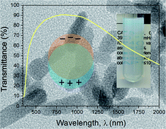
Plasmonic oxide nanocrystals hold great promise in a wide range of applications, for which the availability of scalable and “green” synthesis methods is prerequisite, whereas until recently an excellent response has been demonstrated only for samples prepared through intricate synthesis paths. We report here a simple ethanol solvothermal synthesis route of Al doped ZnO plasmonic nanocrystals (Zn1−xAlxO) at doping levels of x up to 0.15. The obtained Al doped ZnO samples consisted of nanoparticles and short nanorods with a diameter of around 10 nm at x = 0.15 doping level while reaching aspect ratio levels of 50 for lower doping levels. Detailed structural studies using powder X-ray diffraction Rietveld refinement, X-ray absorption and photoelectron spectroscopies show that all samples maintain the structure of the phase-pure zincite with the space group P63mc. The resulting powders exhibit strong infrared absorption while remaining largely transparent for visible light, enabling the preparation of transparent colloidal dispersions. Furthermore, as a test of applicability in a practical device, the nanocrystals were used to prepare transparent piezoresistive Zn0.925Al0.075O–polydimethylsiloxane composites. The prepared sensor material exhibits excellent repeatable and reproducible piezoresistive behaviour.


Introduction

Plasmonic semiconductor oxide nanocrystals such as Al-doped ZnO (AZO),1–3 In-doped ZnO (IZO),3,4 Ga-doped ZnO (GZO),3 Sn-doped In2O3 (ITO),6,7 Sb-doped SnO2 (ATO)8,9 or others10–14 have attracted growing attention due to their applicability in many optoelectronic applications, such as near-infrared selective electrochromic devices,15 (flexible) displays11 and polymer light emitting diodes.4 They also demonstrate excellent bio-sensing and chemical sensing capabilities.16 These materials exhibit localised surface plasmon absorption (LSPA) features in the near-infrared and mid-infrared range due to the resonance frequency of collective oscillations of excess electrons or holes.5 Historically, LSPA is better known for phenomena in nanostructures of noble metals for which the plasmonic band is located in the visible range.17

For oxide semiconductors, LSPA has been most commonly observed in n-type materials with extra conduction band electrons.18 Extra electrons are introduced by aliovalent donor doping where the impurity atoms in a higher charge state replace some host cations in the lattice.1 According to the Drude–Lorentz theory, the absorption will increase and the resonance peak will shift to higher energies with increasing free charge carrier concentration.19 Aliovalent doping is therefore expected to result in a reasonably high LSPA in oxide semiconductors at high doping levels when the host oxide becomes a degenerated semiconductor with high extrinsic electrical conductivity.3 In metals, the resonance frequency of collective oscillations of electrons is sensitive to particle size, shape and properties of the surrounding medium.20 Contrary to metallic nanoparticles, the plasmon resonance frequency of free electrons in doped oxide semiconductors can be varied by changing the dopant type and concentration, thus providing alternative opportunities for plasmonic tailoring of light absorption.21

The synthesis of high quality plasmonic semiconductor oxide nanocrystals is a considerable challenge. The LSPA effect has been observed in semiconductor oxide nanocrystals synthesised by intricate synthetic methods such as hot-injection, which requires metal–organic precursors consisting of an inorganic cluster and coordinating organic ligands.18 Hot-injection is capable of yielding high quality colloidal metal oxide semiconductor nanocrystals with a controlled shape and high doping level, where dopants substitute the targeted atoms in a crystal lattice. However, hot-injection is harsh and not scalable to industrial level. To be able to utilise the effect of LSPA in applications, it is necessary to find ways to use alternative high yield and environmentally-friendly chemical synthesis methods.

The hydrothermal and solvothermal methods are well known solution-based, low-cost synthesis processes that are scalable to mass production.22 Hydrothermal or solvothermal crystal growth is performed in aqueous or non-aqueous hot solutions under high pressure in an autoclave. These synthesis processes are often used to obtain well-ordered crystal structure metal-doped ZnO diluted magnetic semiconductors,23 photocatalysts,24 photoanodes25 and photodetectors.22 Although these routes for the synthesis of AZO nanomaterials have been studied in a number of earlier reports,26–35 to the best of our knowledge, the availability of the LSPA effect in the produced samples has not been previously demonstrated for solvothermally or hydrothermally derived doped ZnO nanocrystals. Meanwhile, high electrical conductivity and LSPA absorption in the infrared range has been observed for high quality AZO, GZO and IZO colloidal nanocrystals obtained by hot-injection synthesis.1–4 In the present article we demonstrate the plasmonic properties of AZO degenerated semiconductor nanocrystals synthesised by a “green” ligand-free solvothermal method using simple Al and Zn salt precursors. AZO has several advantages over other conductive oxides due to the abundance of Zn and Al in nature, low production costs and low toxicity.36

To add to the versatility of the results, the obtained AZO nanocrystals were mixed into polydimethylsiloxane (PDMS) to create a hyperelastic piezoresistive composite sensor material. Hyperelastic piezoresistive composite materials can be used in applications which are out of reach for mechanically rigid technology, such as biomedical devices, wearable strain and motion sensors, smart clothes, and sensory skin for a robotic system. Up to now hyperelastic piezoresistive or tensoresistive sensors have been based on carbon-based37 or metallic filler38 polymer composites, and ferroelectric oxide nanofillers have been used in flexible piezoelectric polymer composites for strain sensing,39 acoustic sensing40 and energy harvesting.41 To the authors’ best knowledge, only Ishigure et al. have investigated oxide based (Sb-doped SnO2 and La0.5Sr0.5CoO3) piezoresistive polymer composites and their electrical properties,42 but until now no plasmonic oxide nanocrystal based piezoresistive polymer composites have been reported that exhibit optical transparency. Here, we demonstrate plasmonic oxide nanocrystals for use as alternative fillers in piezoresistive sensors. As compared to carbonaceous or metallic filler based analogues, this type of system potentially exhibits transmittance in the visible range due to a wide band gap, lower charge carrier concentration and consequent plasmon resonance shift to the infrared spectral range.

Experimental details

ZnO and Al-doped ZnO powders were synthesised using a solvothermal method. Zinc acetate dihydrate (Zn(CH3CO2)2·2H2O) (98%, Sigma Aldrich) was dissolved in 15 ml ethanol (99%, Merck) to obtain a 0.1 M solution. Simultaneously, 30 ml of 0.5 M NaOH (98%, Sigma Aldrich) solution in ethanol was prepared. Both solutions were heated to 80 °C and vigorously stirred in closed glass vials until clear solutions were obtained. The two solutions were mixed and left under stirring at 80 °C for the next 10 h. The mixture was transferred into a 50 ml Teflon-lined stainless steel autoclave, sealed and heated at 150 °C for 24 h. The obtained precipitates were filtered, washed with methanol, and dried in air at 60 °C for 5 h. For doped ZnO synthesis a proportionate amount of Zn(CH3CO2)2·2H2O in ethanol was replaced with Al(NO3)3·9H2O (98%, Sigma Aldrich) to obtain Zn1−xAlxO (where x = 0, 0.025, 0.050, 0.075, 0.100 and 0.150).

The phase composition of the as-synthesised powders was analysed by powder X-ray diffraction (XRD) and Rietveld refinement. The powders were hand-milled in acetone for 5 minutes using an agate mortar and pestle. After drying, some of the material was transferred into a glass capillary of 500 μm in diameter (Mark tube No. 4007805, glass no. 10, Hilgenberg, Malsfeld, Germany) and measured on a Bruker D8 Advance diffractometer (Bruker, Karlsruhe, Germany). The 2θ scan range was 25–120° (step size of 0.0122°) using (Ni and digitally filtered) Cu Kα X-radiation. The counting time of 6.5 seconds per step resulted in a total measurement time of approximately 14 hours per dataset. Rietveld refinement was carried out with the software BGMN version 4.2.22[thin space (1/6-em)]43 and was compared with a wurtzite structure of ZnO published by Kisi and Elcombe.44 Refined parameters included the scale factor, unit cell dimensions a and c, and anisotropic peak broadening. The latter parameter was used by the refinement software to calculate mean crystallite domain sizes.

The X-ray absorption spectroscopy (XAS) and X-ray photoelectron spectroscopy (XPS) experiments were carried out at beamline D1011 of MAX II synchrotron storage ring (Lund, Sweden). The beamline is equipped with a modified SX-700 plane grating monochromator. XPS spectra were measured by an electron energy analyser SCIENTA SES-200 in a fixed analyser transmission (FAT) mode with 200 eV pass energy. The sample was positioned at a normal emission with 40° incident angle for the incoming photon beam. XPS spectra were normalised to the synchrotron ring current to account for the variations in the photon beam intensity. The binding energy scales for XPS experiments were referenced to the C 1s transitions. Zn 2p and Al 2p photoelectron peaks were fitted by asymmetric Gaussian–Lorentzian line shapes after subtracting a Shirley background. The XAS analysis was measured in total electron yield mode, with a spectral resolution of 0.12 eV at the O 1s and 0.33 eV at the Zn 2p threshold regions.

To measure the diffuse light absorbance of powder samples and transmittance of AZO colloids, a UV-Visible Shimadzu UV-3700 spectrophotometer (Shimadzu Scientific Instruments Kyoto, Japan) was used.

Piezoresistive properties were measured for the AZO–PDMS thin films. AZO nanocrystals (15 mg ml−1) were ultrasonically dispersed in a butylamine (20%) and dichloromethane (80%) solution. The desired amount of PDMS (Sylgard 184; Dow Corning, Midland, MI) solution in hexane (10 mg ml−1) and curing agent (Sylgard 184) solution in hexane (1 mg ml−1) were added to the dispersion of AZO nanocrystals. The weight ratio of PDMS to curing agent was 10[thin space (1/6-em)]:[thin space (1/6-em)]1. Before spin coating, 90% by volume of the solvents was evaporated out from the mixture under continuous shaking at room temperature. At the end, 50 μl of the final mixture was spin-coated on the rotating (1500 rpm) glass substrate (2.5 × 2.5 cm), coated by ITO finger electrodes. After spin coating the sample was left at 70 °C for 6 h for curing. After curing, AZO–PDMS film of 5 μm thickness was obtained. ITO electrodes were produced by immersing ITO-covered glass (Rs = 15 Ω sq−1; Kintec, Hong Kong, China) together with a mask into 36.5–38% HCl aqueous solution (Sigma-Aldrich) for 10 min. After etching, the substrate was rinsed with distilled water and the distance between fingers was 350 μm. Electrical resistance change in the cured AZO–PDMS film was measured under applied load as it underwent cyclic loading, applied by tapping the top of the film with a small rubber stack (6 mm in diameter).

Results and discussion

According to the X-ray diffraction data (see Fig. 1) all the samples have phase-pure zincite crystal structure with the space group P63mc (no. 186). Substitution of up to 15% of Zn with Al during the synthesis was not observed to lead to separate Al (oxide) phases. We therefore conclude from the XRD that Al was incorporated into the zincite structure. Anisotropic crystallite size was evident in all samples, with the longest dimension in the direction of the crystallographic c axis (Table 1). Al doping resulted in a significant reduction of the crystallite domain size, leading to increasingly pronounced anisotropic peak broadening with increasing Al concentration, but the elongation along c remained. The shape of the broadened peaks could be approximated, but not accurately modelled by the Rietveld software’s algorithms for crystallite size and micro-strain related peak broadening, which indicated the presence of abundant complex lattice distortions (substitutions and vacancies) in samples with Al substitution. The reduced quality of these datasets rendered a full structure refinement unfeasible, preventing us from more precise localisation and quantification of substitutions and vacancies. A marginal effect of Al doping on the unit cell dimensions was observed. The lattice constant c was approximately 0.1% reduced (Table 1) regardless of the amount of substitution. The a axis, on the other hand, showed initial expansion by +0.02% at 2.5% Al, followed by a gradual shrinkage with increasing Al concentration, eventually becoming 0.028% shorter at 15% Al than the pure ZnO phase.
image file: c5ra11910c-f1.tif
Fig. 1 X-ray diffraction patterns from 0% (bottom) to 15% (top) Al cationic content. The peak positions of the zincite structure model44 are shown at the top of the graph.
Table 1 Crystallographic parameters determined from XRD data by Rietveld refinement. 3σ intervals reported by the Rietveld refinement software are given in parentheses
x (Zn1−xAlxO) a (Å) c (Å) Crystallite size 〈1, 0, 0〉 (nm) Crystallite size 〈0, 0, 1〉 (nm)
0 3.24996 (0.00012) 5.20683 (0.00018) 69.6 (0.9) 140.6 (5.1)
0.025 3.25066 (0.00042) 5.20185 (0.00066) 20.8 (0.3) 71.6 (3.0)
0.050 3.25040 (0.00045) 5.20161 (0.00072) 20.5 (0.3) 75.8 (3.3)
0.075 3.25017 (0.00051) 5.20317 (0.00081) 19.1 (0.3) 67.3 (3.0)
0.100 3.24993 (0.00066) 5.20119 (0.00102) 15.2 (0.3) 51.0 (1.8)
0.150 3.24904 (0.00084) 5.20113 (0.00132) 11.9 (0.2) 38.3 (1.2)


The microstructural features of the solvothermally synthesised pristine and AZO powders were studied by SEM and TEM (Fig. 2). Pristine ZnO sample powder consists of hexagonal single crystalline nanowires with a diameter from 20 to 70 nm, length from 0.2 μm to 1 μm and aspect ratio up to 50. The addition of Al dopant decreased the aspect ratio to the extent that the sample with a composition of Zn0.85Al0.15O consisted of nanoparticles and short nanorods only (Fig. 2(b) and (d)). The length of the Zn0.85Al0.15O nanorods was below 50 nm with a diameter around 10 nm. The average sizes of the nanocrystals of Zn0.85Al0.15O and other compositions were in good agreement with the Rietveld calculation results given in Table 1. The increasing Al loading-related reduction in shape anisotropy can be rationalised via two mechanisms.26 First, according to the Rietveld analysis, the Al doping causes lattice shrinkage along c attributed to the smaller Al3+ (radius 0.53 Å) replacing the larger Zn2+ (radius 0.74 Å), which further leads to a variation of the crystal aspect ratio due to ion diameter effects. Second, the replacement of Zn2+ by Al3+ increases the charge density during nanocrystal growth due to the formation of free electrons, which compensates an excess positive charge from Al3+.26 During hydrothermal synthesis ZnO crystal growth is facilitated by zincate ion (Zn(OH)42−) growth units,45 which may form at high pH values above 12 in accordance with the reaction:

 
image file: c5ra11910c-t1.tif(1)


image file: c5ra11910c-f2.tif
Fig. 2 SEM images of ZnO (a) and Zn0.85Al0.15O (b) and TEM images of ZnO (c) and Zn0.85Al0.15O (d).

The free electrons formed by Zn2+ substitution with Al3+ make it difficult for the zincate ions to diffuse to the crystal surface because of charge repulsion.26

The ZnO and the Zn0.925Al0.075O samples were further characterised using XPS and XAS. Fig. 3 shows the Zn 2p, O 1s, Al 2p and valence band XPS of the ZnO and the Zn0.925Al0.075O nanocrystals. The Zn 2p XPS (Fig. 3(a)) contains the spin–orbit split 2p3/2 and 2p1/2 component bands, with a mutual energy difference of 23.2 (±0.1) eV, with the Zn 2p3/2 binding energy at 1022.0 (±0.2) eV in ZnO and 1021.8 (±0.2) eV in Zn0.925Al0.075O, indicating that Zn is in the 2+ charge state in both samples.46 The O 1s XPS (Fig. 3(b)) contains two partially resolved components at approximately 530 eV and 531.5 eV binding energy. The component at 530 eV corresponds to the O2− ions in the wurtzite structure of ZnO, surrounded by Zn2+ ions (or Zn2+ substituted by Al3+ ions). The photoelectron peak at 531.5 eV is attributed either to the presence of loosely bound oxygen on the surface of the films or it belongs to hydrated oxides. It can also be associated with O2− ions in the oxygen deficient regions within the matrix of ZnO.47 We have observed that the latter component becomes relatively higher for the Zn0.925Al0.075O sample as compared to the undoped ZnO nanowires. The Al 2p (Fig. 3(c)) XPS of the Zn0.925Al0.075O sample contains a single photoelectron peak positioned at 74 eV, indicating that only the Al3+ charge state is present (the metallic Al 2p line at 72.7 eV binding energy is not observed).


image file: c5ra11910c-f3.tif
Fig. 3 XPS spectra measured from the Zn 2p, O 1s, Al 2p and valence band regions of ZnO and Zn0.925Al0.075O nanocrystals.

The O 1s and Zn 2p XAS results are presented in Fig. 4. The Zn 2p edge absorption is virtually identical for the two samples, indicating that the Zn ligand coordination (and sublattice) remains unaffected by Al-doping. The O 1s edge absorption aligns well with previous reports for ZnO48,49 and is overall very similar to the two samples, which indicates a quite perfect preservation of local symmetry and ligand configuration, with a minimal gain in intensity for the Al-doped sample in the energy region; this coincides with the relatively structureless broad band of alumina absorption,50 as a result of the presence of Al 3p–O 2p hybridised states. However, we further noticed that the Al 2p XAS (not shown) of the Zn0.925Al0.075O sample contained only a baseline, with the intense and structured alumina (α-Al2O3) features50 absent, indicating that no segregation of alumina occurred in the sample.


image file: c5ra11910c-f4.tif
Fig. 4 Zn 2p (top panel) and O 1s (lower panel) X-ray absorption of the ZnO (solid line) and the Zn0.925Al0.075O (dashed line) nanocrystals.

Fig. 5 (left panel) shows the UV-NIR absorption spectra of the ZnO and AZO samples. The AZO nanopowders with different Al content show strong absorption in the NIR region, while pristine ZnO exhibits a sharp absorption edge below 400 nm, while it is transparent in the visible and IR regions. The appearance of absorption in the NIR region for the AZO samples is a clear indication of the LSPA effect.51 The observed LSPA in the AZO samples can be regarded as an indication that the increase of free electron density upon Zn2+ substitution by Al3+ can be directly assessed from the optical properties. Zinc substitution by Al3+ can be expected to give rise to the formation of various point defects, the majority of which would be zinc vacancies (VZn2−), Al3+ on Zn2+ sites (AlZn1+), oxygen interstitials (Oi2−) or freestanding electrons trapped at an anion lattice vacancy (e). In AZO materials obtained under oxidising conditions, an AlZn1+ defect is compensated either by a VZn2− or an Oi2− in accordance to eqn (2) and (3), respectively.

 
image file: c5ra11910c-t2.tif(2)
 
image file: c5ra11910c-t3.tif(3)
where OO stands for a regular oxygen site.


image file: c5ra11910c-f5.tif
Fig. 5 Left panel: UV-NIR absorption spectra (Kubelka–Munk function) for different AZO samples. Right panel: The optical transmittance spectrum of Zn0.85Al0.15O colloid solution in a mixture of butylamine (20%) and dichloromethane (80%). The inset shows a photograph of the concentrated stock colloid (15 mg ml−1), which was 10 times diluted for the transmittance measurement.

Since these pathways will not give the (detached, trapped electron) e defects, it appears that in order to increase the density of (quasi) free charge carriers in the AZO, the synthesis should be carried out under non-oxidising conditions,52 where generation of the e defects proceeds according to

 
image file: c5ra11910c-t4.tif(4)
and becomes preferable. This will have a bearing on the LSPA behaviour and related plasmonic of the material.

In order to probe the effect of synthesis environment on the plasmonic behaviour of the obtained samples, the samples were tested using UV-vis absorption. First, the Zn0.85Al0.15O nanocrystals were used to produce visible light transparent colloidal dispersions. Fig. 5 (right panel) shows the transmittance spectrum and photograph of the Zn0.85Al0.15O colloidal solution in a mixture of butylamine (20%) and dichloromethane (80%). The colloid of Zn0.85Al0.15O nanocrystals shows strong absorption in the near-infrared region.

The optical absorption behaviour of the synthesised samples shows that free electron formation in AZO materials is favoured in ethanol solvothermal synthesis. The NIR absorption initially increases with increasing Al dopant concentration until it attains the strongest NIR absorption for the Zn0.925Al0.075O sample. At even higher dopant levels, however, the NIR absorption instead decreases again. The possible causes for this latter decrease at higher Al concentration probably stem from the lowered sample definition at high Al concentrations, which can favour the formation of non-reducible defect clusters that would act as recombination centres and cause loss of produced charge carriers.53

In order to test the overall applicability of our results in the case of practical devices, the obtained Zn0.925Al0.075O nanocrystals were mixed into PDMS to create a hyperelastic piezoresistive sensor composite material. According to percolation theory, conductive fillers in an insulating matrix, above a critical volume fraction (percolation threshold), form a conductive network in a polymer matrix. The highest piezoresistive effect is expected at filler concentrations slightly above the percolation threshold where the electric resistance changes most abruptly with filler concentration.54 Fig. 6(a) shows the percolation behaviour of the Zn0.925Al0.075O/PDMS composite. The percolation threshold is comparatively high (ϕ ∼ 20%), which is attributed to a low aspect ratio of the nanofillers as well as a weak tendency to build aggregates and subsequently conductive channels in the polymer matrix. The most well-known piezoresistive hyperelastic sensors are carbon black filled elastomers, which have percolation thresholds above 10%.55 At the same time, graphene filled composites have a percolation threshold below 1%, attributed to the graphene high aspect ratio ∼1000.37 Fig. 6(b) shows the performance of our piezoresistive sensor with repeated loading–unloading of pressure. As expected, the ohmic resistance decreased during the application of the compressive external load. The change in resistance under external load can be interpreted as an indication of the creation of new or the destruction of existing conductive networks.56 In piezoresistive elastomer composites with low aspect ratio fillers the divergence of adjacent particles and the destruction of existing networks is more probable.57 Our sensor material shows fast response–recovery behaviour as well, with the resistance either rapidly decreasing or restored to the initial value after applying or removing the external mechanical load. The output signals were highly repeatable and reproducible over multiple cycle tests, indicating their potential for applications in real-time monitoring. The produced sensor device shows (limited) transparency even in the visible range (see inset of Fig. 6(a)).


image file: c5ra11910c-f6.tif
Fig. 6 Percolation behaviour (a) and piezoresistive performance (b) of the Zn0.925Al0.075O/PDMS composite.

Overall, the obtained AZO/PDMS composites can be spin coated on transparent flexible electrodes to further produce transparent and flexible pressure sensors. This appears to be in line with the presently growing demand in numerous applications to replace the present essentially brittle and rigid devices with lightweight, mechanically flexible and transparent next generation electronic appliances.58 From a different aspect, thin films made of such conductive wide band gap semiconductor oxides will probably exhibit higher transmittance in the visible range compared to metal or carbon based counterparts.

Conclusions

Zn1−xAlxO nanocrystals with excellent plasmonic response were produced using a “green” ethanol-based solvothermal synthesis route. The synthesis of undoped ZnO yields nanowires. The Al content was observed to have an effect on the shape and aspect ratio of the produced nanoparticles: while the synthesis of undoped ZnO yielded long nanowires with aspect ratios of up to 50, increasing the Al content gradually decreases the aspect ratio to slightly above 1 (almost isotropic growth) at Al content x = 0.15. Powder XRD Rietveld refinement, XAS and XPS revealed all samples exhibit the phase-pure zincite crystal structure with the space group P63mc. Diffuse reflectance measurements showed the appearance of localised surface plasmon absorption in the NIR region for all with a maximum at x = 0.075 Al-loaded samples. The Zn0.85Al0.15O nanocrystals were used to make visible light transparent colloidal dispersions, which absorbed light in the UV and NIR range. For the first time, a hyperelastic piezoresistive sensor composite material was obtained by mixing the Zn0.925Al0.075O nanocrystals into polydimethylsiloxane. This sensor material was transparent in the visible range and shows a fast piezoresistive response and recovery, with the resistance decreased and restored rapidly to the initial value after applying and removing an external mechanical pressure.

Acknowledgements

This work was supported by the Estonian Research Council (post-doctoral research grant PUTJD108 and IUT2-25) and the Estonian Centre of Excellence in Research Projects “High-technology Materials for Sustainable Development” TK117 and “Mesosystems: Theory and Applications” TK114. The research leading to these results received funding from the European Community’s Seventh Framework Programme (FP7/2007–2013) CALIPSO under grant agreement no. 312284 and from the Baltic Science Link project coordinated by the Swedish Research Council.

Notes and references

  1. A. M. Schimpf, S. T. Ochsenbeina, R. Buonsanti, D. J. Milliron and D. R. Gamelin, Chem. Commun., 2012, 48, 9352–9354 RSC.
  2. R. Buonsanti, A. Llordes, S. Aloni, B. A. Helms and D. J. Milliron, Nano Lett., 2011, 11, 4706–4710 CrossRef CAS PubMed.
  3. E. D. Gaspera, A. S. R. Chesman, J. van Embden and J. J. Jasieniak, ACS Nano, 2014, 8, 9154–9163 CrossRef PubMed.
  4. X. Liang, Y. Ren, S. Bai, N. Zhang, X. Dai, X. Wang, H. He, C. Jin, Z. Ye, Q. Chen, L. Chen, J. Wang and Y. Jin, Chem. Mater., 2014, 26, 5169–5178 CrossRef CAS.
  5. G. Garcia, R. Buonsanti, E. L. Runnerstrom, R. J. Mendelsberg, A. Llordes, A. Anders, T. J. Richardson and D. J. Milliron, Nano Lett., 2011, 11, 4415–4420 CrossRef CAS PubMed.
  6. S. D. Lounis, E. L. Runnerstrom, A. Bergerud, D. Nordlund and D. J. Milliron, J. Am. Chem. Soc., 2014, 136, 7110–7116 CrossRef CAS PubMed.
  7. A. M. Schimpf, S. D. Lounis, E. L. Runnerstrom, D. J. Milliron and D. R. Gamelin, J. Am. Chem. Soc., 2015, 137, 518–524 CrossRef CAS PubMed.
  8. U. zum Felde, M. Haase and H. Weller, J. Phys. Chem. B, 2000, 104, 9388–9395 CrossRef CAS.
  9. J. M. Xu, L. Li, S. Wang, H. L. Ding, Y. X. Zhang and G. H. Li, CrystEngComm, 2013, 15, 3296–3300 RSC.
  10. B. T. Diroll, T. R. Gordon, E. A. Gaulding, D. R. Klein, T. Paik, H. J. Yun, E. D. Goodwin, D. Damodhar, C. R. Kagan and C. B. Murray, Chem. Mater., 2014, 26, 4579–4588 CrossRef CAS.
  11. L. De Trizio, R. A. Buonsanti, A. M. Schimpf, A. Llordes, D. R. Gamelin, R. Simonutti and D. J. Milliron, Chem. Mater., 2013, 25, 3383–3390 CrossRef CAS.
  12. A. Agrawal, I. Kriegel and D. J. Milliron, J. Phys. Chem. C, 2015, 119, 6227–6238 CAS.
  13. B. Tandon, G. Shiva Shanker and A. Nag, J. Phys. Chem. Lett., 2014, 5, 2306–2311 CrossRef CAS.
  14. S. Ghosh, M. Saha, V. D. Ashok, B. Dalal and S. K. De, J. Phys. Chem. C, 2015, 119, 1180–1187 CAS.
  15. T. E. Williams, C. M. Chang, E. L. Rosen, G. Garcia, E. L. Runnerstrom, B. L. Williams, B. Koo, R. Buonsanti, D. J. Milliron and B. A. Helms, J. Mater. Chem. C, 2014, 2, 3328–3335 RSC.
  16. Y. Aksu, S. Frasca, U. Wollenberger, M. Driess and A. Thomas, Chem. Mater., 2011, 23, 1798–1804 CrossRef CAS.
  17. J. M. Luther, P. K. Jain, T. Ewers and A. P. Alivisatos, Nat. Mater., 2011, 10, 361–366 CrossRef CAS PubMed.
  18. R. Buonsanti and D. J. Milliron, Chem. Mater., 2013, 25, 1305–1317 CrossRef CAS.
  19. A. M. Schimpf, N. Thakkar, C. E. Gunthardt, D. J. Masiello and D. R. Gamelin, ACS Nano, 2014, 8, 1065–1072 CrossRef CAS PubMed.
  20. S. Linic, P. Christopher and D. B. Ingram, Nat. Mater., 2011, 10, 911–921 CrossRef CAS PubMed.
  21. S. D. Lounis, E. L. Runnerstrom, A. Llordes and D. J. Milliron, J. Phys. Chem. Lett., 2014, 5, 1564–1574 CrossRef CAS.
  22. C. L. Hsu and S. J. Chang, Small, 2014, 10, 4562–4585 CrossRef CAS PubMed.
  23. G. Clavel, M.-G. Willinger, D. Zitoun and N. Pinna, Adv. Funct. Mater., 2007, 17, 3159–3169 CrossRef CAS PubMed.
  24. S. Yang, C. Ge, Z. Liu, Y. Fang, Z. Li, D. Kuang and C. Su, RSC Adv., 2011, 1, 1691–1694 RSC.
  25. S. Ameen, M. S. Akhtar, H.-K. Seo, Y. S. Kim and H. S. Shin, Chem. Eng. J, 2012, 187, 351–356 CrossRef CAS PubMed.
  26. R. Chen, P. Zhu, L. Deng, T. Zhao, R. Sun and C. Wong, ChemPlusChem, 2014, 79, 743–750 CrossRef CAS PubMed.
  27. Z. Lu, J. Zhou, A. Wang, N. Wang and X. Yang, J. Mater. Chem., 2011, 21, 4161–4167 RSC.
  28. S. Yun, J. Lee, J. Yang and S. Lim, Phys. B, 2010, 405, 413–419 CrossRef CAS PubMed.
  29. J. T. Chen, J. Wang, R. F. Zhuo, D. Yan, J. J. Feng, F. Zhang and P. X. Yan, Appl. Surf. Sci., 2009, 255, 3959–3964 CrossRef CAS PubMed.
  30. R. R. Piticescu, R. M. Piticescu and C. J. Monty, J. Eur. Ceram. Soc., 2006, 26, 2979–2983 CrossRef CAS PubMed.
  31. S. N. Bai, H. H. Tsai and T. Y. Tseng, Thin Solid Films, 2007, 516, 155–158 CrossRef CAS PubMed.
  32. M. Mazilu, N. Tigau and V. Musat, Opt. Mater., 2012, 34, 1833–1838 CrossRef CAS PubMed.
  33. N. Ye and C. C. Chen, Opt. Mater., 2012, 34, 753–756 CrossRef CAS PubMed.
  34. C.-L. Hsu, C.-W. Sua and T.-J. Hsueh, RSC Adv., 2014, 4, 2980–2983 RSC.
  35. T. Wang, Y. Liu, G. Li, Z. Sun, J. Lu, B. Liub and M. Wu, CrystEngComm, 2011, 13, 2661–2666 RSC.
  36. R. G. Gordon, MRS Bull., 2000, 25, 52–57 CrossRef CAS.
  37. C. S. Boland, U. Khan, C. Backes, A. O’Neill, J. McCauley, S. Duane, R. Shanker, Y. Liu, I. Jurewicz, A. B. Dalton and J. N. Coleman, ACS Nano, 2014, 8, 8819–8830 CrossRef CAS PubMed.
  38. M. Park, J. Im, M. Shin, Y. Min, J. Park, H. Cho, S. Park, M.-B. Shim, S. Jeon, D.-Y. Chung, J. Bae, J. Park, U. Jeong and K. Kim, Nat. Nanotechnol., 2012, 7, 803–809 CrossRef CAS PubMed.
  39. H. Gullapalli, V. S. M. Vemuru, A. Kumar, A. Botello-Mendez, R. Vajtai, M. Terrones, S. Nagarajaiah and P. M. Ajayan, Small, 2010, 6, 1641–1646 CrossRef CAS PubMed.
  40. G.-T. Hwang, M. Byun, C. K. Jeong and K. J. Lee, Adv. Healthcare Mater., 2015, 4, 646–658 CrossRef CAS PubMed.
  41. A. Šutka, M. Timusk, V. Kisand, A. Šutka and E. Dauksta, Int. J. Appl. Ceram. Technol., 2015, 12, E117–E121 CrossRef PubMed.
  42. Y. Ishigure, S. Iijima, H. Iot, T. Ota, H. Unuma, M. Takahashi, Y. Hikichi and H. Suzuki, J. Mater. Sci., 1999, 34, 2979–2985 CrossRef CAS.
  43. T. Taut, R. Kleeberg and J. Bergmann, Mater. Struct., 1998, 5, 57–66 Search PubMed.
  44. E. H. Kisi and M. M. Elcombe, Acta Crystallogr., Sect. C: Cryst. Struct. Commun., 1989, 45, 1867–1870 CrossRef.
  45. W.-J. Li, E.-W. Shi, W.-Z. Zhong and Z.-W. Yin, J. Cryst. Growth, 1999, 203, 186–196 CrossRef CAS.
  46. J. F. Moulder, W. F. Stickle, P. E. Sobol and K. D. Bomben, in Handbook of X-ray Photoelectron Spectroscopy, ed. J. Chastain and R. C. King, Physical Electronics, Eden Prairie, 1st edn, 1992, p. 89 Search PubMed.
  47. J. Mass, P. Bhattacharya and R. S. Katiyar, Mater. Sci. Eng., B, 2003, 103, 9–15 CrossRef.
  48. J. G. Chen, Surf. Sci. Rep., 1997, 30, 1–152 CrossRef CAS.
  49. J.-H. Guo, L. Vayssieres, C. Persson, R. Ahuja, B. Johansson and J. Nordgren, J. Phys.: Condens. Matter, 2002, 14, 6969 CrossRef CAS.
  50. T. Jõgiaas, T. Arroval, L. Kollo, J. Kozlova, T. Käämbre, H. Mändar, A. Tamm, I. Hussainova and K. Kukli, Phys. Status Solidi A, 2014, 211, 403–408 CrossRef PubMed.
  51. A. Comin and L. Manna, Chem. Soc. Rev., 2014, 43, 3957–3975 RSC.
  52. P.-C. Yao, S.-T. Hang, Y. Lin, W.-T. Yenb and Y.-C. Lin, Appl. Surf. Sci., 2010, 257, 1441–1448 CrossRef CAS PubMed.
  53. O. Warschkow, D. E. Ellis, G. B. González and T. O. Mason, J. Am. Ceram. Soc., 2003, 86, 1707–1711 CrossRef CAS PubMed.
  54. M. Knite, V. Teteris, A. Kiploka and J. Kaupuzs, Sens. Actuators, A, 2004, 110, 142–149 CrossRef CAS PubMed.
  55. M. Hindermann-Bischoff and F. Ehrburger-Dolle, Carbon, 2001, 39, 375–382 CrossRef CAS.
  56. J. Hwang, J. Jang, K. Hong, K. N. Kim, J. H. Han, K. Shin and C. E. Park, Carbon, 2011, 49, 106–110 CrossRef CAS PubMed.
  57. M. Hussain, Y. H. Choa and K. Niihara, Composites, Part A, 2001, 32, 1689–1696 CrossRef.
  58. D. Choi, M.-Y. Choi, W. M. Choi, H.-J. Shin, H.-K. Park, J.-S. Seo, J. Park, S.-M. Yoon, S. J. Chae, Y. H. Lee, S.-W. Kim, J.-Y. Choi, S. Y. Lee and J. M. Kim, Adv. Mater., 2010, 22, 2187–2192 CrossRef CAS PubMed.

This journal is © The Royal Society of Chemistry 2015