
Hole-transport-material-free perovskite solar cells based on nanoporous gold back electrode†
Xiaoxin Zhoua,
Chunxiong Baoa,
Faming Lia,
Hao Gaoa,
Tao Yu*abc,
Jie Yanga,
Weidong Zhua and
Zhigang Zouabc
aNational Laboratory of Solid State Microstructures & Eco-Materials and Renewable Energy Research Center (ERERC) at Department of Physics, Nanjing University, Nanjing 210093, P. R. China. E-mail: yutao@nju.edu.cn
bCollaborative Innovation Center of Advanced Microstructures, Nanjing University, Nanjing 210093, P. R. China
cJiangsu Key Laboratory for Nano Technology, Nanjing 210093, P. R. China
First published on 30th June 2015
Abstract
Easily fabricated, directly transferred thin nanoporous gold was first used as a back electrode for hole-transport-material-free perovskite solar cells. In order to infiltrate CH3NH3PbI3 into the pores of mesoporous layers and the nanoporous gold back electrode, three ways, namely one-step spin-coating deposition, sequential deposition, and two-step spin-coating deposition were introduced to fabricate CH3NH3PbI3. The devices containing well infiltrated CH3NH3PbI3 show the highest power conversion efficiency of 7.99%.
Introduction
Metal–organic halide perovskite CH3NH3PbI3 was first introduced to the photovoltaic field by Kojima and his co-workers in 2009.1 But solar cells with perovskite CH3NH3PbI3 as light harvester did not attract worldwide attention until 2012, when their power conversion efficiency reached around 10% due to the introduction of Spiro-OMeTAD as a hole-transport-material (HTM).2,3 In the past years, highly efficient perovskite solar cells fabricated by different ways such as sequential deposition,4 vapor deposition,5 and the vapor assisted solution process6 have been reported, and the highest reported efficiency reached 20.1% in the year 2015.7 The rapid evolution of perovskite solar cells is benefited by the intrinsic properties of CH3NH3PbI3 such as direct band gap, large absorption coefficient,8 high carrier mobility,9 long carrier diffuse length,10,11 and ambipolar charge transport.3,12Despite the rapid development in device efficiency, many problems still hinder perovskite solar cells from practical application, such as expensive HTM and complex thermal vapor deposit process. Most of the highly efficient perovskite solar cells contain expensive HTM, which largely increase the fabrication costs. HTM-free perovskite solar cell is a promising candidate for avoiding the above problem. Fortunately, the hole-transport property of perovskite CH3NH3PbI3 makes it possible. Etgar and his co-workers first reported CH3NH3PbI3/TiO2 solar cell with the efficiency of 5.5% without using HTM.12 Meng and his co-workers reported HTM-free perovskite solar cells and confirmed that TiO2/CH3NH3PbI3/Au cell is a typical heterojunction solar cell.13 Due to the work function of gold is well matched to perovskite CH3NH3PbI3, most HTM-free perovskite solar cells use gold as back electrode. But the gold back electrode often fabricated by high vacuum thermal vapor deposition, which makes the fabrication process complex. Mhaisalkar et al. reported directly transferred carbon nanotube network instead of gold back electrode for perovskite solar cell, but the carbon nanotube network was synthesized by chemical vapor deposition at a high temperature of 1150 °C which made the process complex and expensive.14 Han and his co-workers reported porous carbon as back electrode instead of thermal deposited gold electrode.15,16 But the conductivity of carbon electrode is far lower than gold electrode thus the devices made by Han et al. with a thick porous carbon layer of about 10 μm which may limit the practical use. To date, gold is still the best candidate material for the back electrode of HTM-free perovskite solar cells because of its high electrical conductivity and well matched work function with the perovskite CH3NH3PbI3. Thus a special shaped gold contains the following features can be a good candidate for the back electrode of HTM-free perovskite solar cells: easily fabricated, directly transferred, porous structured.
Nanoporous gold (NPG) is a material with 3-dimensional porous structure and the size of the pores is in the nanoscale. In the past ten years, NPG has gradually attracted widespread attention in chemical/biological sensors,17 and also for electronic devices18 due to its unique properties of high electrical conductivity and high specific surface area combined with chemical stability.19 De-alloying method was used to fabricate NPG, which made the fabrication process simple. Easily fabricated, porous structured, high electrical conductivity and well matched work function make it a good candidate for the application in HTM-free perovskite solar cells.
Herein, we report HTM-free perovskite solar cells using easily fabricated, directly transferred thin NPG as back electrode. NPG film was directly transferred onto the device, exempting the energy consumption of thermal vapor deposition process. The thickness of the NPG electrode was much thinner than porous carbon electrode. In order to get efficient devices, three deposition ways were introduced to fabricate CH3NH3PbI3. The infiltration and crystallinity of CH3NH3PbI3 by different fabricate ways and the influence on the devices performance were investigated.
Results and discussion
Fig. 1a shows the schematic structure of the HTM-free perovskite solar cell with NPG back electrode. Similar to porous carbon electrode based HTM-free perovskite solar cells, the NPG electrode was porous structured and the structure of our device is similar to that of Han et al.15,16 A compact TiO2 layer was deposited on the etched FTO glass. Mesoporous TiO2 and Al2O3 layers were deposited successively on the compact TiO2 layer. After that the NPG back electrode was direct transferred onto the mesoporous substrates, then the perovskite CH3NH3PbI3 was infiltrated into the pores of mesoporous layers and NPG by different methods. Fig. 1b shows the energy-level alignment of the devices. Under the radiation of the sunlight, CH3NH3PbI3 absorbs the sunlight then electron–hole pairs generate. The electron–hole pairs separate with the electrons inject from the conduction band of CH3NH3PbI3 into the conduction band of TiO2 than transport to FTO and the holes inject from CH3NH3PbI3 into NPG electrode. | ||
| Fig. 1 (a) Schematic structure of HTM-free perovskite solar cells based on nanoporous gold electrode (NPG), (b) energy-level alignment of NPG based perovskite solar cells, (c) SEM image of NPG fabricated by de-alloying, (d) SEM image of PbI2 deposited on the porous structure of mesoporous layers and NPG. | ||
De-alloying, a facile way to selectively dissolve one or more components from a metallic solid solution, was used to prepare NPG. The raw material (Ag/Au alloy leaf) was etched in HNO3, thus Ag was dissolved by HNO3 and the remained Au formed a 3-dimensional disordered porous structure which was showed in Fig. 1c. The size of the pores is about 30–40 nm. The thickness of the NPG we obtained is about 100–200 nm which was the same as that of the raw alloy films, which is much thinner than thick porous carbon electrode. This porous structured NPG back electrode can provide large contact area between CH3NH3PbI3 and the electrode. The 3-dimensional continuous disordered porous structure makes the NPG remain the high conductivity of gold. Simultaneously, this size of the pore and the continuous porous structure make the precursor infiltrated into the pores of mesoporous layer and NPG possible. As demonstrated in Fig. 1d, the PbI2 can filled the porous structure well.
There are many factors influence the performance of the devices, such as the pore size of the NPG, the thickness of the mesoporous layer and so on. The last step of the device fabrication process, which is the deposition of CH3NH3PbI3 into the porous structure, will also impact the performance of the device. In this work, we investigate the influence of infiltration and crystallinity of CH3NH3PbI3 deposited by different ways on the performance of the devices. To guarantee the comparability of different CH3NH3PbI3 deposition methods, we optimized the other factors and keep invariant in all devices.
Fig. 2 shows the X-ray diffraction (XRD) patterns of the porous structured substrate and CH3NH3PbI3 deposited on the substrate by different ways. The XRD patterns show that the diffraction peaks at 26.4°, 38.2°, 44.3° and 51.5° can be attributed to the substrate. The diffraction peak at 12.59° was attributed to PbI2.7 Intense diffraction peaks at 14.08°, 28.40°, 31.86° can be assigned to (110), (220), (310) diffractions of CH3NH3PbI3 respectively.20 All the samples fabricated by different ways show the characteristic peaks of CH3NH3PbI3. The characteristic peaks of PbI2 appeared in the XRD pattern of the sample fabricated by two-step spin-coating deposition. The intensity of the characteristic peaks of CH3NH3PbI3 fabricated by two-step spin-coating deposition is weaker than that of CH3NH3PbI3 fabricated by the rest two ways. Thus we conclude that the crystallinity of CH3NH3PbI3 fabricated by one-step spin-coating deposition and sequential-deposition were better, while the crystallinity of CH3NH3PbI3 fabricated by two-step spin-coating deposition was relatively poor.
 | ||
| Fig. 2 XRD patterns of the porous structure substrate and CH3NH3PbI3 fabricated by three different ways: one-step spin-coating deposition, sequential deposition, two-step spin-coating deposition. | ||
Fig. 3 shows the top surface SEM images of CH3NH3PbI3 fabricated by three different ways: one-step spin-coating deposition (Fig. 3a and d), sequential deposition (Fig. 3b and e), two-step spin-coating deposition (Fig. 3c and f), Fig. 3d–f are the enlargement images of Fig. 3a–c, respectively. Through one-step spin-coating deposition, we obtained needle-like morphology on the top surface of the NPG electrode, which is the same as fabricated on the mesoporous TiO2.4,21 The NPG was covered with big CH3NH3PbI3 grains in some area while in other area little CH3NH3PbI3 were filled in the pores of NPG. In both sequential deposition and two-step spin-coating deposition methods, PbI2 were first infiltrated into the porous structure. As showed in Fig. 1d, PbI2 were filled in the pores, which is the prerequisite of the following step. CH3NH3PbI3 fabricated by sequential deposition shows cubic grain on the top surface of NPG, which shows the similar morphology of the reference.4 Similar to one-step spin-coating deposition, the NPG was covered with cubic-shaped CH3NH3PbI3 grains in some area, while some other area filled little CH3NH3PbI3. CH3NH3PbI3 fabricated by two-step spin-coating deposition shows well infiltrated morphology. There exist no big CH3NH3PbI3 grains on the top surface of NPG, most CH3NH3PbI3 were filled in the pores of NPG. Two-step spin-coating deposition method provides a larger contact area between CH3NH3PbI3 and NPG.
 | ||
| Fig. 3 SEM images of the top surfaces of CH3NH3PbI3 fabricated by one-step spin-coating deposition (a and d), sequential deposition (b and e) and two-step spin-coating deposition (c and f). (d–f) are the enlargement images of (a–c), respectively. | ||
For HTM-free perovskite solar cells, CH3NH3PbI3 act simultaneously as light absorber and HTM. Photogenerated holes were transport from CH3NH3PbI3 to back electrode directly.12,22 Due to the sunlight were illuminated from the FTO side, and the electron–hole pairs were mainly generated in the CH3NH3PbI3 filled in the mesoporous layers. CH3NH3PbI3 filled in the pores of NPG and contact with the bottom surface of NPG mainly act the role of HTM. CH3NH3PbI3 on the top surface have no exact function for the devices. Thus the infiltration of CH3NH3PbI3 into the mesoporous layer and NPG is necessary in our device.
In order to confirm that CH3NH3PbI3 can infiltrate into mesoporous layers, cross section images of the devices were photographed. Fig. 4 shows cross section images of CH3NH3PbI3 fabricated by three different ways: one-step spin-coating deposition (Fig. 4a), sequential deposition (Fig. 4b), and two-step spin-coating deposition (Fig. 4c). The images show that CH3NH3PbI3 were infiltrated into the mesoporous layer by all fabrication ways. Simultaneously, the images show that CH3NH3PbI3 were infiltrated in the pores of NPG, although the top surface images show little CH3NH3PbI3 were infiltrated in the pores in some area. But in the area where covered with CH3NH3PbI3, the pores of NPG were filled with CH3NH3PbI3, which showed in the cross section images.
 | ||
| Fig. 4 SEM images of cross section of perovskite solar cells based on nanoporous gold (NPG) electrode deposited by three different ways: (a) one-step spin-coating deposition, (b) sequential deposition, (c) two-step spin-coating deposition. | ||
The SEM images show that CH3NH3PbI3 fabricated by two-step spin-coating deposition infiltrated better into NPG than one-step spin-coating deposition and sequential deposition, but the XRD pattern shows poor crystallinity with the presence of PbI2 impurity phase. To investigate the performance of devices fabricated by different ways, we measure the efficiency of all devices. Fig. 5 shows the J–V curves of NPG electrode based HTM-free perovskite solar cells. J–V curves of devices fabricated by one-step spin-coating deposition, sequential deposition, and two-step spin-coating deposition were showed in Fig. 5a–c, respectively. The best efficient devices were fabricated by two-step spin-coating deposition, which shows the efficiency of 7.99%, with the JSC = 15.0 mA, the VOC = 0.86 V and the FF = 61.8%. The devices fabricated by one-step spin-coating deposition and sequential deposition show the efficiency of 3.5% and 5.8% respectively, although the CH3NH3PbI3 filled in the pores of NPG were not enough. Thus we consider that the amount of CH3NH3PbI3 filled in the pores and the effective contact area between CH3NH3PbI3 and NPG impact the device performance largely. Of course, the crystallinity of CH3NH3PbI3 will impact the performance in some degree, but we confirm the contact between CH3NH3PbI3 and pores plays more important role to the performance.
 | ||
| Fig. 5 J–V curves of HTM-free perovskite solar cells with and without mesoporous Al2O3 for three different deposition methods: (a) one-step spin-coating deposition, (b) sequential deposition, (c) two-step spin-coating deposition. | ||
Both devices with and without mesoporous Al2O3 layer were fabricated, and their J–V curves were also show in Fig. 5. In all the three ways fabricated devices, both the JSC and VOC of the devices with mesoporous Al2O3 are higher than that of devices without mesoporous Al2O3. The efficiency of the devices with mesoporous Al2O3 is higher than that without mesoporous Al2O3. This phenomenon can be explained as follows. When the devices contain no mesoporous Al2O3, TiO2 will contact with NPG, which will lead to electron–hole recombination. The recombination will promote the decrease of JSC and VOC, thus the efficiency will be decrease. Al2O3 is a type of insulator with large band gap of about 7–9 eV, in which charge cannot transport. Fabricate a mesoporous Al2O3 layer between TiO2 and NPG can avoid the direct contact of TiO2 and NPG, then the probability of electron–hole recombination can be reduce. Thus the efficiency can be improved with the use of mesoporous Al2O3.
In perovskite solar cells, an anomalous hysteresis in the J–V curves were widely observed.23,24 To investigate the J–V curves hysteresis of our devices, we measured the J–V curves at different scan directions which were showed in Fig. 6. Fig. 6a and b show the J–V hysteresis of the devices fabricated by two-step spin-coating deposition with and without mesoporous Al2O3, respectively. Fig. 6c and d show the J–V hysteresis of the devices fabricated by sequential deposition and one-step spin-coating deposition, respectively. It shows that the devices fabricated by different ways all present almost negligible hysteresis. The devices without mesoporous Al2O3 show slight larger hysteresis than which with mesoporous Al2O3. The same phenomenon of hysteresis has been observed by Han et al.16,25 So we consider that the slight hysteresis in our devices may attribute to the special structure of the devices, which is similar to that of the devices made by Han et al.
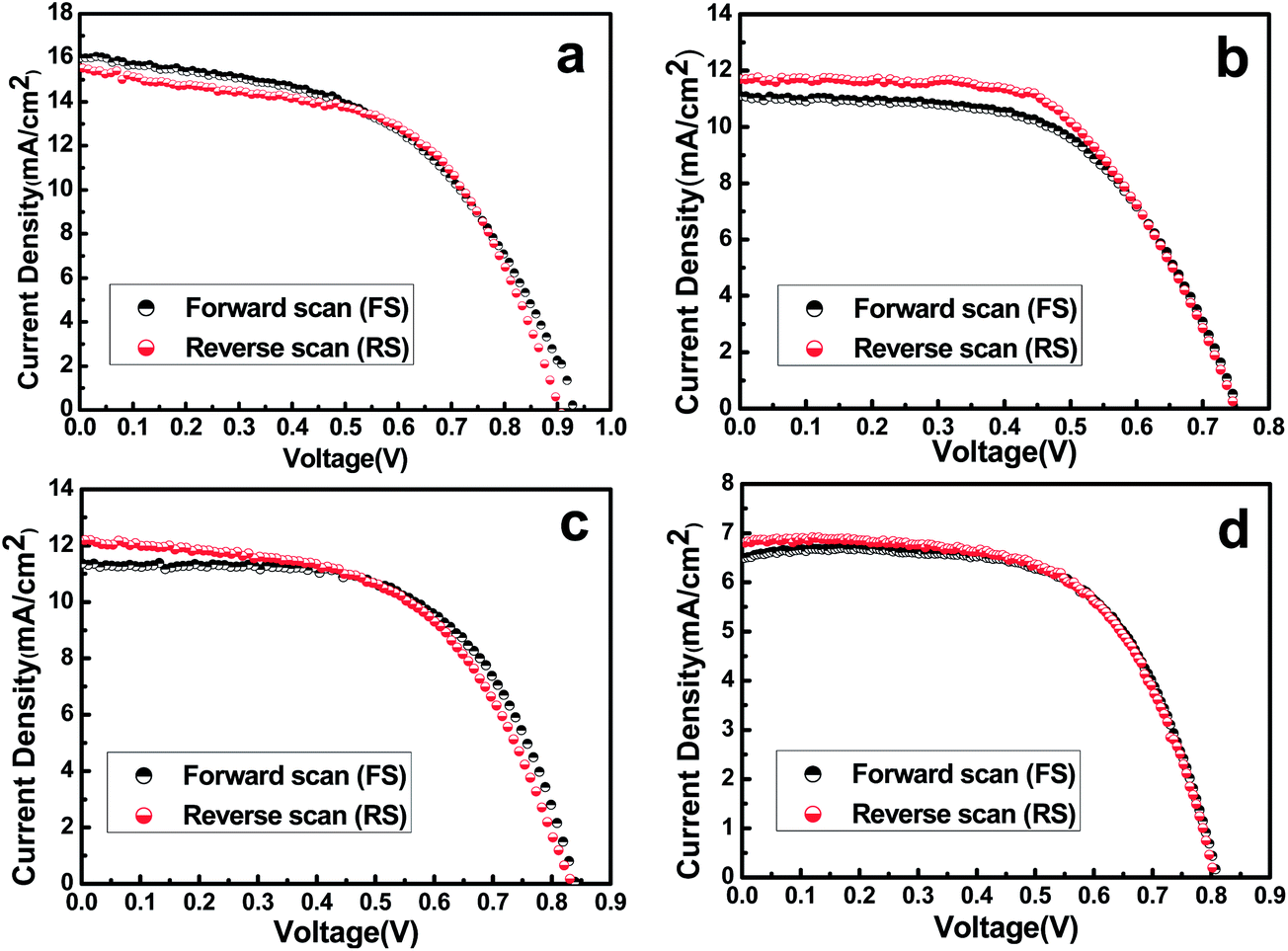 | ||
| Fig. 6 J–V curves measured at forward scan (FS, from short-circuit to open-circuit under the forward bias voltage) and reverse scan (RS, from open-circuit to short-circuit under the forward bias voltage) for the devices fabricated by (a) two-step spin-coating deposition (with Al2O3), (b) two-step spin-coating deposition (without mesoporous Al2O3), (c) sequential deposition (with Al2O3) and (d) one-step spin-coating deposition (with Al2O3). | ||
To investigate the reproducibility of the devices fabrication, we present the parameter statistic of 20 devices fabricated by two-step spin-coating deposition in Fig. 7. The statistical method was the same as the previous work.26 The 20 devices were fabricated from one batch. The best devices show the efficiency of 7.99%, with JSC = 15.0 mA cm−2, VOC = 0.86 V, FF = 61.8%. The average JSC, VOC, FF and Eff are 15.10 ± 1.30 mA cm−2, 0.86 ± 0.06 V, 56.9 ± 6.0%, 7.44 ± 0.54%, respectively.
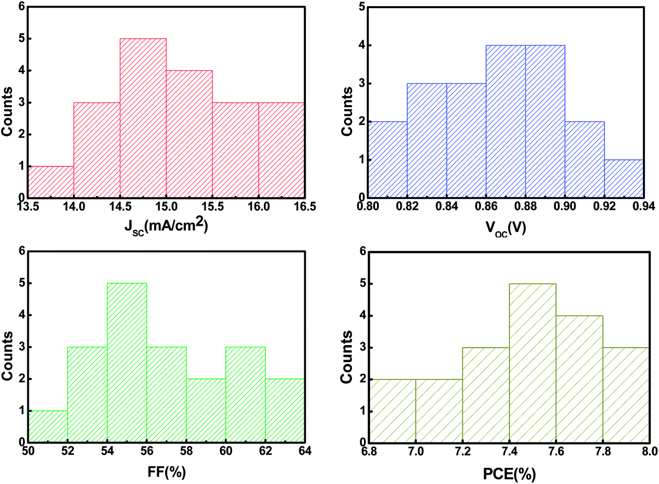 | ||
| Fig. 7 Solar cells photovoltaic parameters statistics based on 20 devices fabricated by two-step spin-coating deposition in one batch. | ||
Conclusion
In summary, we have fabricated HTM-free perovskite solar cells based on easily fabricated, directly transferred thinner NPG back electrode. The HTM-free perovskite solar cells based on NPG electrode show the highest power conversion efficiency of 7.99% with reliable reproducibility. The effects of infiltration and crystallization of CH3NH3PbI3 fabricated by different deposition ways on the performance of the devices were investigated. The infiltration of CH3NH3PbI3 into the porous structure is a critical factor of the device. Two-step spin-coating deposition fabricated devices shows better infiltrated CH3NH3PbI3 and the best performance but poor crystallinity. With the use of mesoporous Al2O3, the performance can improved largely. The hysteresis of J–V curves in our devices is not obvious which may attribute to the special structure of the devices. To further optimize the deposition process to get a well infiltrated and crystallization perovskite CH3NH3PbI3, the power conversion efficiency especially the JSC and VOC would be improve. Thus the NPG can be a good candidate for back electrode of HTM-free perovskite solar cells.Acknowledgements
This work was supported primarily by the national Natural Science Foundation of China (11174129 and 61377051), the National Basic Research Program of China (2011CB933303 and 2013CB632404), the Science and Technology Research Program of Jiangsu Province (BK20130053). We thank Dr Xiangyang Wang and Dr Zhiqiang Wang for their experimental and technical assistance.Notes and references
- A. Kojima, K. Teshima, Y. Shirai and T. Miyasaka, J. Am. Chem. Soc., 2009, 131, 6050–6051 CrossRef CAS PubMed.
- H. S. Kim, C. R. Lee, J. H. Im, K. B. Lee, T. Moehl, A. Marchioro, S. J. Moon, R. Humphry-Baker, J. H. Yum, J. E. Moser, M. Gratzel and N. G. Park, Sci. Rep., 2012, 2, 591 Search PubMed.
- M. M. Lee, J. Teuscher, T. Miyasaka, T. N. Murakami and H. J. Snaith, Science, 2012, 338, 643–647 CrossRef CAS PubMed.
- J. Burschka, N. Pellet, S. J. Moon, R. Humphry-Baker, P. Gao, M. K. Nazeeruddin and M. Gratzel, Nature, 2013, 499, 316–319 CrossRef CAS PubMed.
- M. Liu, M. B. Johnston and H. J. Snaith, Nature, 2013, 501, 395–398 CrossRef CAS PubMed.
- Q. Chen, H. Zhou, Z. Hong, S. Luo, H.-S. Duan, H.-H. Wang, Y. Liu, G. Li and Y. Yang, J. Am. Chem. Soc., 2014, 136, 622–625 CrossRef CAS PubMed.
- W. S. Yang, J. H. Noh, N. J. Jeon, Y. C. Kim, S. Ryu, J. Seo and S. I. Seok, Science, 2015, 348, 1234–1237 CrossRef CAS PubMed.
- S. De Wolf, J. Holovsky, S.-J. Moon, P. Löper, B. Niesen, M. Ledinsky, F.-J. Haug, J.-H. Yum and C. Ballif, J. Phys. Chem. Lett., 2014, 5, 1035–1039 CrossRef CAS.
- C. Wehrenfennig, G. E. Eperon, M. B. Johnston, H. J. Snaith and L. M. Herz, Adv. Mater., 2014, 26, 1584–1589 CrossRef CAS PubMed.
- S. D. Stranks, G. E. Eperon, G. Grancini, C. Menelaou, M. J. P. Alcocer, T. Leijtens, L. M. Herz, A. Petrozza and H. J. Snaith, Science, 2013, 342, 341–344 CrossRef CAS PubMed.
- G. Xing, N. Mathews, S. Sun, S. S. Lim, Y. M. Lam, M. Gratzel, S. Mhaisalkar and T. C. Sum, Science, 2013, 342, 344–347 CrossRef CAS PubMed.
- L. Etgar, P. Gao, Z. Xue, Q. Peng, A. K. Chandiran, B. Liu, M. K. Nazeeruddin and M. Gratzel, J. Am. Chem. Soc., 2012, 134, 17396–17399 CrossRef CAS PubMed.
- J. Shi, J. Dong, S. Lv, Y. Xu, L. Zhu, J. Xiao, X. Xu, H. Wu, D. Li, Y. Luo and Q. Meng, Appl. Phys. Lett., 2014, 104, 063901 CrossRef PubMed.
- Z. Li, S. A. Kulkarni, P. P. Boix, E. Shi, A. Cao, K. Fu, S. K. Batabyal, J. Zhang, Q. Xiong, L. H. Wong, N. Mathews and S. G. Mhaisalkar, ACS Nano, 2014, 8, 6797–6804 CrossRef CAS PubMed.
- Z. Ku, Y. Rong, M. Xu, T. Liu and H. Han, Sci. Rep., 2013, 3, 3132 Search PubMed.
- A. Mei, X. Li, L. Liu, Z. Ku, T. Liu, Y. Rong, M. Xu, M. Hu, J. Chen, Y. Yang, M. Gratzel and H. Han, Science, 2014, 345, 295–298 CrossRef CAS PubMed.
- K. Hu, D. Lan, X. Li and S. Zhang, Anal. Chem., 2008, 80, 9124–9130 CrossRef CAS PubMed.
- R. Y. Zhang, H. A. Andersson, M. Andersson, B. Andres, H. Edlund, P. Edstrom, S. Edvardsson, S. Forsberg, M. Hummelgard, N. Johansson, K. Karlsson, H. E. Nilsson, M. Norgren, M. Olsen, T. Uesaka, T. Ohlund and H. Olin, Sci. Rep., 2013, 3, 7 Search PubMed.
- A. Wittstock, J. Biener and M. Baeumer, Phys. Chem. Chem. Phys., 2010, 12, 12919–12930 RSC.
- T. Baikie, Y. Fang, J. M. Kadro, M. Schreyer, F. Wei, S. G. Mhaisalkar, M. Graetzel and T. J. White, J. Mater. Chem. A, 2013, 1, 5628 CAS.
- Y. Zhao and K. Zhu, J. Phys. Chem. C, 2014, 118, 9412–9418 CAS.
- W. A. Laban and L. Etgar, Energy Environ. Sci., 2013, 6, 3249 CAS.
- H. J. Snaith, A. Abate, J. M. Ball, G. E. Eperon, T. Leijtens, N. K. Noel, S. D. Stranks, J. T.-W. Wang, K. Wojciechowski and W. Zhang, J. Phys. Chem. Lett., 2014, 5, 1511–1515 CrossRef CAS.
- E. L. Unger, E. T. Hoke, C. D. Bailie, W. H. Nguyen, A. R. Bowring, T. Heumueller, M. G. Christoforo and M. D. McGehee, Energy Environ. Sci., 2014, 7, 3690–3698 CAS.
- M. Hu, L. Liu, A. Mei, Y. Yang, T. Liu and H. Han, J. Mater. Chem. A, 2014, 2, 17115–17121 CAS.
- W. Zhu, T. Yu, F. Li, C. Bao, H. Gao, Y. Yi, J. Yang, G. Fu, X. Zhou and Z. Zou, Nanoscale, 2015, 7, 5427–5434 RSC.
Footnote |
| † Electronic supplementary information (ESI) available. See DOI: 10.1039/c5ra11720h |
| This journal is © The Royal Society of Chemistry 2015 |