
Synthesis of photocatalytic hematite nanotube array using a template-free solvothermal approach
Jiqing Jiao*a,
Jianguo Tang*a,
Guoming Wanga,
Yao Wanga,
Linjun Huanga,
Zhen Huanga,
Jixian Liua,
Yukun Zhua and
Laurence A. Belfioreb
aInstitute of Hybrid Materials, National Base of International S. & T. Cooperation on Hybrid Materials and Growing Base for State Key Laboratory, Teachers College, Qingdao University, 308 Ningxia Road, Qingdao 266071, P. R. China. E-mail: jiaojq@qdu.edu.cn; jianguotangde@hotmail.com; Fax: +86 532 85951519; Tel: +86 532 85951519
bDepartment of Chemical and Biological Engineering, Colorado State University, Fort Collins, Colorado 80523, USA
First published on 9th July 2015
Abstract
The paper describes a template-free solvothermal synthesis of α-Fe2O3 hollow nanotube arrays over a large area. The columnar nanotubes on the substrate have closed tips and smooth defined walls. The thickness of the nanowall is about 10 nm, which could offer short diffusion distances and decrease recombination of electron–hole pairs. And the preferential orientation is the [110] axis. The cubic Au nanocrystals were decorated by a photocatalytic reduction process, and the corresponding EDX mappings intuitively display the distributions of the composites. Au nanocrystals matched the absorption of α-Fe2O3 hollow nanotube arrays, which improved photoactivity under visible light (wavelength > 420 nm). The photoactivity of the sample was investigated based on systematic photoelectrochemical (PEC) measurements. These revealed that the photocurrent density of Au/α-Fe2O3 is almost 6 times higher than that of pure α-Fe2O3. And its photocurrent density increases to 0.16 mA cm−2 at 1.23 VRHE under irradiation. The mechanism of enhanced visible light PEC activity has been discussed using schematics. Hence, the study presents not only a route for formation of α-Fe2O3 hollow nanotube arrays but also PEC applications of plasmonic composites.
Introduction
Even since E. Becquerel discovered the photoelectric effect in 1839, the conversion of solar to chemical fuels or electric power using semiconductor electrodes has been a topic of great interest for several decades.1–4 Among the most studied materials,5 hematite (α-Fe2O3) is one of the most promising candidates for application in photoelectrochemical (PEC) water splitting6 owing to its abundance,7 stability8 and environmental compatibility.9 And the favorable band gap (2.2 eV) makes it absorb roughly 38% of the solar radiation under air mass 1.5 globe.10 Its valence b and edge position is also located at a suitable energy for oxygen evolution in water photooxidation. Unfortunately, several factors mean it has lower photoelectric efficiencies: fast recombination of photogenerated charge carries, short diffusion length for holes (2–4 nm), low hole mobility at room temperature (0.01 cm2 V−1 s−1),11 slow oxygen evolution reaction kinetics, low flat band potential,12 overpotential (0.4–0.6 V)13 et al.Recently, efforts have been made to enhance the photoelectric performance of hematite. Among those methods, heteroatom doping and architecture tuning have been two major solutions employed to improve its photoelectric efficiency. Various heteroatom incorporation (such as Co,14 Pt,15 Ni,16 Ti17 and Si et al.) are certainly beneficial for increasing the mobility of charge transport and improving photoactivity. However, the most active absorbing hematite nanodomains should be within nanometer (∼10 nm) distance from the semiconductor to electrolyte interface, and sufficient effective thickness of materials is retained to absorb much of the solar light.18 Furthermore, only the charge carriers close to the surface could be successfully transferred into semiconductor–electrolyte junction. Besides impurity doping, controlling the morphology with sizes comparable to hole-diffusion length scale is efficient strategy to separate photoexcited carriers.19 Among the various morphologies, the hollow structured hematite (hollow sphere and nanotube) can markedly shorten the path of photogenerated carriers and increase the efficiency of photoelectron.16 The thin nanowalls would help to improve the activity significantly compared to other nanostructures. Currently, there are a number of synthetic strategies of inorganic nanotubule including direct assembly, template-directed growth, electrochemical anodization et al.20 Nevertheless, there is still a big challenge to develop well-defined vertically hollow nanoarrays on large-area solid substrates. Apart from above approaches, the plasmonic composites of noble metal and semiconductors have been investigated due to localized surface plasmon resonance (LSPR).21 Gold (Au) nanoparticles have been attracted much attention owing to tunable plasmon resonances, large optical cross sections and stable property et al.22 It's important to improve the activity by tuning the size of Au nanoparticles, which matches with hematite absorption.23–25
In this report, we described a facile synthesis of vertically α-Fe2O3 hollow nanotube arrays via template-free route on fluorine-doped tin oxide (FTO) glass. Compared with traditional nanotubes, the hollow nanotube arrays had closed tips and smooth defined wall on substrate. The hematite hollow nanotube arrays have been seldom reported without template. And then Au nanocrystals were deposited on α-Fe2O3 intersurface. Its absorption matched with the α-Fe2O3 prepared, which can improve the absorption ability and photoelectric activity. Hence, the study is contributed to plasmonic nanocomposites for PEC applications.
Experimental
All chemical reagents are analytical (AR) grade. And all aqueous solutions were prepared with deionized water. The hematite hollow nanotube arrays is prepared on FTO glass, and the glasses are cleaned ultrasonically in ethanol and deionized water, respectively.The preparation of Au/α-Fe2O3 hollow nanotube arrays as following:
0.170 g NaNO3 (0.05 M), 0.324 g FeCl3 (0.10 M) and 0.016 g NaF (0.10 M) was dissolved in 20 mL deionized water with stirring. And then the red solution was transferred into the PTFE reactor. FTO glass was put into the prepared solution. The PTFE reactor was put into the stainless steel autoclave, which was then sealed. The reaction was maintained at 95 °C for 6 hours. The yellow layer of iron oxyhydroxides (FeOOH) film was formed on the FTO glass, and it was subsequently washed with deionized water. And then it's annealed at 550 °C for 2 hours.
The Au nanocrystals were deposited by photocatalytic reduction method. The FTO glasses with α-Fe2O3 were soaked in 0.3 mM HAuCl4 aqueous for 24 hours. And then the sample was irradiated in 0.3 mM solution with 300 W Xe lamp for 1 hour to reduce the absorbed Au3+ to Au by photocatalysis.
Characterization
The X-ray diffraction (XRD) pattern was recorded on a D8 (Bruker, Germany) X-ray diffractometer with graphite monochromator Cu Kα radiation (l = 1.54178). Scanning electron microscopy (SEM) was carried out with JSM-6700F (Japan). And energy dispersive X-ray (EDX) and EDX mapping were performed on INCA Energy (Oxford). Transmission electron microscopy (TEM) image and high-resolution TEM (HRTEM) image were performed on a JEM-2010HR field emission transmission electron microscope (JEOL, Japan). UV-vis absorption spectra were measured on UV-vis-NIR spectrophotometer UV-3150 (SHIMADZU, Japan). All the measurements were performed at room temperature.Photoelectrochemical characterization
Photocurrent was measured in a three-electrode configuration with 1 mol L−1 KOH (pH = 13.6) as electrolyte, Ag/AgCl/sat. KCl as reference, and a platinum plate was counter electrode. The linear sweep voltammograms (I–V), photoelectric response (amperometric I–t) and electrochemical impedance spectroscopy (EIS) and Mott–Schottky measurements were measured by electrochemical workstation (CHI760C). The potential of the photoelectrode is reported against the reversible hydrogen electrode (RHE):| ERHE = EAgCl + 0.059 pH + EoAgCl with EoAgCl = 0.1976 V at 25 °C |
A 300 W Xe illuminator (Peking Changtuo, PLS- 3XE300) with a cutoff filter to remove light of wavelengths below 420 nm was used as the simulated sunlight.
Result and discussion
Crystal information of various samples is studied by XRD pattern in Fig. 1. The mainly diffraction peaks from SnO2 coating of the glass substrate could be seen from XRD pattern without annealing. No characterization peaks of crystal are observed before annealing besides substrate, which means that hematite crystals can't be synthesized on FTO glass. The hematite peaks26 corresponding to (104), (110) and (300) plans27 can be seen after annealing, (red pattern), consistent with powder standards (no. 33-0664).28 The Au nanocrystals were deposited on the surface of α-Fe2O3 by photocatalytic reduction process. Apart from peaks from SnO2 and α-Fe2O3, the Au peaks can be clearly observed, corresponding to three typical peaks of (111), (200) and (220) crystal planes.23 The cubic structure was determined (no. 65-2870).29 Furthermore, the significant broadening of diffraction peaks might be ascribed to the very small crystallite size of α-Fe2O3 and Au nanoparticles, similar to our previously reported.30 | ||
| Fig. 1 XRD patterns of without annealing sample (black), hematite (red) and Au/hematite (green). The diffraction peaks of SnO2, hematite and Au are indicated by ▲, ﹟ and *, respectively. | ||
As shown in Fig. 2, the morphology and structure could be determined by SEM and TEM measurement. After annealing, the columnar nanoarray of α-Fe2O3 is revealed in Fig. 2a. And its diameter and length are about 50 and 200 nm, respectively (top inset). Fig. 2b is the top-view section, and the well-defined nanoarrays can be clearly seen. The detail information and more evidence of the nanostructure are characterized by TEM measurement. The hollow nanotubes can be clearly shown in Fig. 2c. The columnar nanotube has closed tips and smooth defined wall on substrate (bottom inset), and its diameter and length are the some size with SEM images (top inset). As can be seen in Fig. 2d, its thickness of nanowall is about 10 nm, which could offer short diffusion distances and decrease recombination of electron–hole.31 The HRTEM images of the hollow nanotube is shown in inset of Fig. 2d it displays regular lattice fringes with a spacing of 0.25 nm, corresponding to the (110) lattice plane of hematite. It indicates a preferential orientation of the [110] axis, which the best orientation for hematite structure with good conductivity.32 The reaction process would be deduced as the following:
| Fe3+ + 3F− → FeF3 |

the FeOOH would be deposited on the surface of FTO glass, and the FeF3(H2O)18 is prepared on substrate when the F− is added into the solution. The α-Fe2O3 would be formed by decomposition of FeOOH and FeF3(H2O) when annealing temperature was 550 °C. The following reactions are responsible for forming of hollow nanotube arrays. Thus, the well-defined hollow nanotube arrays were synthesized via template-free route.

 | ||
| Fig. 2 Morphology and structure of hematite. (a) Hollow nanotube arrays of α-Fe2O3, the top inset is the corresponding cross section. (b) Morphology of top-view section. (c) TEM images of hollow nanotubes (top inset) and nanotube arrays (bottom inset). (d) TEM and HRTEM images. | ||
The Au nanocrystals were decorated on hematite surface by photocatalytic reduction. After modification with Au nanoparticles, the morphology of sample is revealed in Fig. 3a. The Au nanoparticles with size of 60 nm can be distinguished (red circle), which is agreement with previous report.29 To intuitively display the Au distribution, the EDX mapping of various elements were carried out. Fig. 3b presents the SEM images and the corresponding EDX mappings of elements Fe, O and Au, respectively. The red, blue and green colours are distribution of Fe, O and Au elements, respectively. It's easy to find that the coverage of green colour (Au) has distribution on interface of hematite arrays. The plasmonic system is further characterized by the EDX pattern in Fig. 3c. The EDX pattern demonstrates that the product consists of four elements. Sn peaks were about at 3.0 keV and 3.5 keV, which is from the substrate SnO2.8 The O peak at about 0.5 keV can be observed. Obviously, the Fe peaks were at 0.7 keV, 6.4 keV and 7.0 keV, respectively. And the Au peaks is around 2.1 keV. In addition, the Au content of the sample approximates 1.24 wt% by EDX analysis. Based on experimental analysis, composites Au/α-Fe2O3 hollow nanotube arrays were synthesized successfully. Au nanocrystals can strongly interact with visible light, which can improve the sunlight absorption markedly.
 | ||
| Fig. 3 (a) SEM image of composites Au/α-Fe2O3. (b) SEM images and the corresponding EDX maps of elements Fe, O and Au. (c) EDX spectrum for the Au/α-Fe2O3. | ||
The absorption of Au/α-Fe2O3 was characterized by UV-vis absorption spectroscopy. The Fig. 4 presents the absorption spectra of α-Fe2O3, Au/α-Fe2O3 and Au, respectively. The bleak curve is the absorption spectrum of α-Fe2O3 hollow nanotube arrays, the peak at 550–600 nm is attributed to the characteristic absorption of hematite. After Au nanoparticles modification, the composite display broad absorption among visible range (red curve). The green line is broad absorption around 630 nm of Au nanoparticles,33 the wavelength is larger than absorption of α-Fe2O3. The hollow nanotube arrays prepared indicates improving photoactivity with Au modification. General speaking, the plasmonic composites Au/α-Fe2O3 have provided enhanced property by energy transfer, scattering24 and hot electrons transfer process.25 The scattering process would occur at Au particles with size of 100 nm. It's reported that the absorption wavelengths of α-Fe2O3 for energy transfer process.24 For hot electron/hole transfer injection, enhancements can occur at energies below the semiconductor band gap. This provides a key distinguishing characteristic of hot electron/hole transfer.24
 | ||
| Fig. 4 UV-vis spectra of α-Fe2O3, Au/α-Fe2O3 and Au nanocrystals (dotted line), inset is IPCE of Au/α-Fe2O3. The inset is digital images of FeOOH, α-Fe2O3 and Au/α-Fe2O3 from left to right, respectively. | ||
To evaluate enhanced activity of photoanodes designed under irradiation, Xe lamp with 420 nm cutoff filter as light source, systematic PEC measurements were carried out. The photocurrent response of the two samples were evaluated by amperometric I–t curves,13 which was collected with light on or off cycles without voltage. As shown in Fig. 5a, the irradiation time is taken for 20 s each time. When the illumination is interrupted, the photocurrent rapidly drops to original value of steady state. The current responds with the turn-on and turn-off of the light quickly. The photocurrent arises from the photoinduced charge separation of composites, and the charge transportation process is very rapid. Obviously, the photocurrent density of pure α-Fe2O3 is 13.2 μA cm−2. The photocurrent density of Au/α-Fe2O3 increases to 78.6 μA cm−2. It reveals that photocurrent density of Au/α-Fe2O3 is almost 6 times higher than that of pure α-Fe2O3. In addition, the photocurrent has initial spike current when light was turned on and off, and then the photocurrent quickly returned to steady state. The spike current arises from photoelectron recombination with surface-trapped holes or photooxidation intermediates.
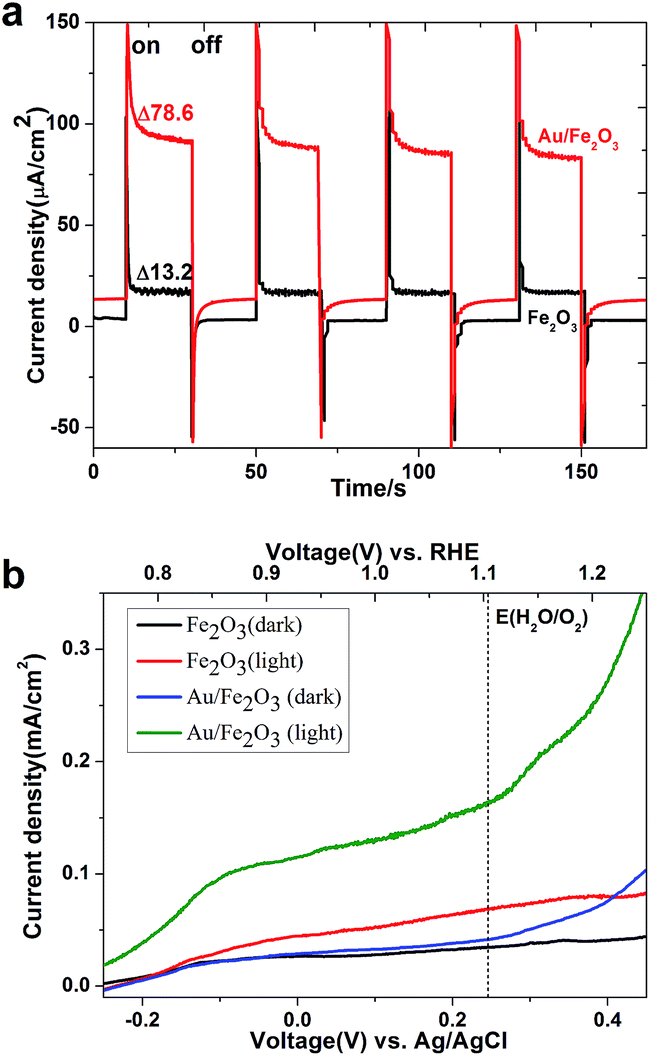 | ||
| Fig. 5 Photocurrent response (a) and current–voltage (b) of nanotube arrays of α-Fe2O3 and Au/α-Fe2O3 under darkness and illumination, respectively. | ||
As following, current–voltage dependence32 is shown in Fig. 5b under darkness and illumination, respectively. As to α-Fe2O3, the dark current (black line) displays onset potential at 0.75 VRHE, and the current density increases to 0.02 mA cm−2 at 0.90 VRHE. The almost saturation current density keep constant value until 1.23 VRHE. And its photocurrent density starts on 0.75 VRHE and increases to 0.07 mA cm−2 at 1.23 VRHE. As to Au/α-Fe2O3, its current is emerged at about 0.75 VRHE, and the current rise to 0.04 mA cm−2 slowly until 1.2 VRHE under darkness. The onset potential voltage displays anode-shift compared with hematite, and the photocurrent climbs to 0.16 mA cm−2 at 1.23 VRHE under illumination. Obviously, Au/α-Fe2O3 exhibits prominent higher photocurrent than hematite. The Au nanocrystals play an important role in the absorption of light and separation of photoelectron–hole. Thus, the structure could improve electron transfer interface of photoanode during photooxidation process.
The kinetics of photoelectrochemical process at electrode surface was investigated by EIS measurements and Mott–Schottky analysis, which can help us to understand the charge transport properties of Au/α-Fe2O3 electrodes.34 Fig. 6a displays its EIS spectra.4 The x axis and y axis represent the real part of impedance (Z′) and imaginary part of the impedance (Z′′), respectively. The Au/α-Fe2O3 electrode displays one semicircle at the high-frequency and a straight line at the low-frequency region at open circuit, which indicates that the electrochemical reaction at electrode is controlled by a mix process of charge transfer and diffusion. But the capacitive arc of Au/α-Fe2O3 is much smaller under illumination. It shows that photoexcited carrier transfer resistance in the Au/α-Fe2O3 markedly decrease, which increases the photocurrent density and charge transfer during the PEC process.
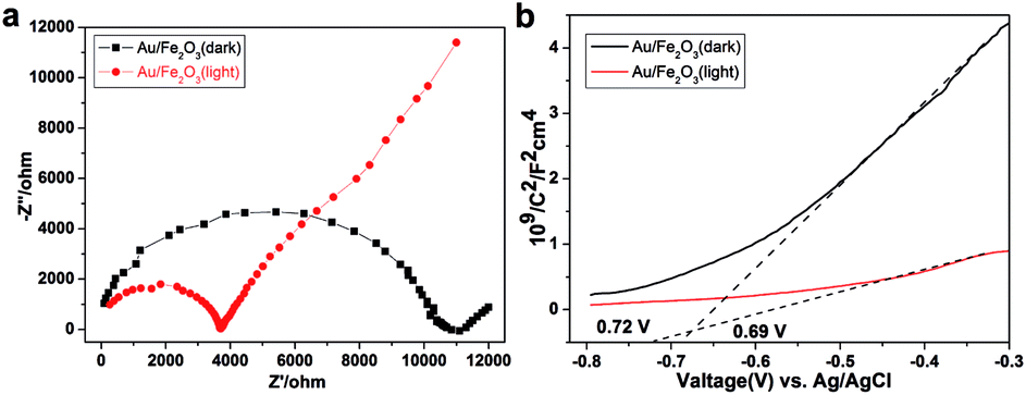 | ||
| Fig. 6 EIS (a) and Mott–Schottky plots (b) of Au/α-Fe2O3 under darkness and illumination. | ||
The capacitance of the Au/α-Fe2O3 is further investigated by Mott–Schottky theory,35 which was commonly used to determine both donor density and flat band potential at the semiconductor/electrolyte interface.36 The capacitance of hematite is described by the following equation:11
| (1/C)2 = (2/e0εε0Nd)(E − EFB − κT/e0) |
| Nd = (2/e0εε0)[d(1/C2)/dV]−1 |
The positive slope indicated that α-Fe2O3 is n-type semiconductor. Under illumination and darkness, the Nd was deduced to be about 1.5 × 1020 cm−3 and 2.1 × 1021 cm−3, respectively.
Based on the above discussion, reasons behind the better photoresponse and higher photocurrent density of designed composites are explained by schematics (Fig. 7).25 An incident photon is absorbed directly by an n-type semiconductor, creating a hole in the valence band (VB) and an electron in the conduction band (CB). The Au nanocrystals are irradiated by visible light, oscillation of free electrons can be induced due to plasmonic resonance,37 which can improve the sunlight absorption markedly.
 | ||
| Fig. 7 Schematic of charge carrier transfer on Au/α-Fe2O3 surface under visible light irradiation (>420 nm). | ||
On the one hand, the near-field electromagnetic field emerges closed Au nanoparticles, and then overlap enhanced electrical fields are formed around Au nanoparticles. It promotes the electrons are excited from VB to CB of α-Fe2O3, which can increase the light harvesting around visible region. On the other hand, the hot electrons would be excited from Fermi energy level of Au, and the hot electrons with higher energy would be injected into CB of the adjacent α-Fe2O3.24 As an antenna, and it can be improved the photoactivity by hot electron injection. Thus, the absorption of light can be confined to the near-surface region of semiconductor, recombination can be minimized because the minority carriers can travel short distance. The two major factors make hematite hollow nanotube arrays have higher photoactivity work at visible range.38 Thus Au/α-Fe2O3 can effectively increase sunlight absorption, separate photo-electrons and photo-holes and improve the photoactivity during PEC process.
Conclusions
The well-defined α-Fe2O3 hollow nanotube arrays were fabricated successfully via template-free method. The columnar nanotube arrays had closed tips and smooth defined wall on FTO glass. And its thickness of nanowall is about 10 nm, which could offer short diffusion distances and decrease recombination of electron–hole pair. The HRTEM displays the a preferential orientation of the [110] axis. The cubic Au nanocrystals were deposited by photocatalytic reduction process. And corresponding EDX mappings exhibit elements distribution. Au nanocrystals coupled with the band gap of hematite owing to LSPR, which matched with absorption of α-Fe2O3 nanotube arrays. The Au/α-Fe2O3 is designed for improving visible light photoactivity. The photo activities were investigated based on systematic PEC measurements. The photocurrent response of Au/α-Fe2O3 indicates the higher value (78.6 μA cm−2), the value is almost 6 times than pure α-Fe2O3. And its photocurrent increases to 0.16 mA cm−2 at 1.23 VRHE. The photocurrent density and charge transfer were revealed under illumination by EIS and Mott–Schottky analysis. Obviously, the plasmonic composite had better photoresponse and higher photocurrent density, its mechanism was explained by schematics. And of course, the photocurrent is low under visible range, thus the work will further be studied to improve photoelectron–hole separation and electrode transfer interface of photoanode during PEC process.Acknowledgements
We are grateful to Mr Kexiao Ji and Mr Pengfei Chen for help for experimental support. The work was financially supported by the National Natural Science Foundation (no. 51403114 and 51273096), Shandong Province Natural Science Founding (BS2014CL025) and China Postdoctoral Science Foundation (no. 2014M560536).Notes and references
- Z. Zhang, M. F. Hossain and T. Takahashi, Int. J. Hydrogen Energy, 2010, 35(16), 8528–8535 CrossRef CAS PubMed.
- A. Fujishima, Science, 2003, 301, 1673 CrossRef CAS PubMed.
- Z. Wang, D. Luan, S. Madhavi, Y. Hu and X. W. Lou, Energy Environ. Sci., 2012, 5(1), 5252–5256 CAS.
- A. Kay, I. Cesar and M. Grätzel, J. Am. Chem. Soc., 2006, 128(49), 15714–15721 CrossRef CAS PubMed.
- J. Jiao, J. Xia, W. Qiu, J. Tang, G. Li, D. Kuang, Y. Tong and L. Chen, Electrochim. Acta, 2014, 136, 217–222 CrossRef CAS PubMed.
- F. E. Osterloh, Chem. Soc. Rev., 2013, 42(6), 2294–2320 RSC.
- P. M. Kouotou, Z. Y. Tian, H. Vieker, A. Beyer, A. Golzhauser and K. Kohse-Hoinghaus, J. Mater. Chem. A, 2013, 1(35), 10495–10504 CAS.
- P. Wang, D. Wang, J. Lin, X. Li, C. Peng, X. Gao, Q. Huang, J. Wang, H. Xu and C. Fan, ACS Appl. Mater. Interfaces, 2012, 4(4), 2295–2302 CAS.
- X. Zhang, Y. Chen, H. Liu, Y. Wei and W. Wei, CrystEngComm, 2013, 15(31), 6184–6190 RSC.
- V. Lorenzelli, G. Busca and N. Sheppard, J. Catal., 1980, 66(1), 28–35 CrossRef CAS.
- D. D. Qin, C. L. Tao, S. I. In, Z. Y. Yang, T. E. Mallouk, N. Bao and C. A. Grimes, Energy Fuels, 2011, 25(11), 5257–5263 CrossRef.
- X. Mou, X. Wei, Y. Li and W. Shen, CrystEngComm, 2012, 14(16), 5107–5120 RSC.
- F. Le Formal, K. Sivula and M. Grätzel, J. Phys. Chem. C, 2012, 116(51), 26707–26720 CAS.
- J. Jiao, L. Chen, D. Kuang, W. Gao, H. Feng and J. Xia, RSC Adv., 2011, 1(2), 255–261 RSC.
- Z. Zhang, M. F. Hossain, T. Miyazaki and T. Takahashi, Environ. Sci. Technol., 2010, 44(12), 4741–4746 CrossRef CAS PubMed.
- W. Cheng, J. He, Z. Sun, Y. Peng, T. Yao, Q. Liu, Y. Jiang, F. Hu, Z. Xie, B. He and S. Wei, J. Phys. Chem. C, 2012, 116(45), 24060–24067 CAS.
- S. Shen, C. X. Kronawitter, D. A. Wheeler, P. Guo, S. A. Lindley, J. Jiang, J. Z. Zhang, L. Guo and S. S. Mao, J. Mater. Chem. A, 2013, 1(46), 14498–14506 CAS.
- L. Li, Y. Yu, F. Meng, Y. Tan, R. J. Hamers and S. Jin, Nano Lett., 2012, 12(2), 724–731 CrossRef CAS PubMed.
- M. Zhang, Y. Lin, T. J. Mullen, W. F. Lin, L. D. Sun, C. H. Yan, T. E. Patten, D. Wang and G. Y. Liu, J. Phys. Chem. Lett., 2012, 3(21), 3188–3192 CrossRef CAS.
- J. Liu, Y. Li, H. Fan, Z. Zhu, J. Jiang, R. Ding, Y. Hu and X. Huang, Chem. Mater., 2009, 22(1), 212–217 CrossRef CAS.
- L. Wu, F. Li, Y. Y. Xu, J. W. Zhang, D. Q. Zhang, G. S. Li and H. X. Li, Appl. Catal., B, 2015, 164, 217–224 CrossRef CAS PubMed.
- W. J. Chen, Y. H. Lu, W. Dong, Z. Chen and M. R. Shen, Mater. Res. Bull., 2014, 50, 31–35 CrossRef CAS PubMed.
- D. D. Zhao, Y. L. Yu, H. J. Long and Y. A. Cao, Appl. Surf. Sci., 2014, 315, 247–251 CrossRef CAS PubMed.
- S. C. Warren and E. Thimsen, Energy Environ. Sci., 2012, 5(1), 5133–5146 CAS.
- S. T. Kochuveedu, D. P. Kim and D. H. Kim, J. Phys. Chem. C, 2011, 116(3), 2500–2506 Search PubMed.
- N. T. Hahn, H. Ye, D. W. Flaherty, A. J. Bard and C. B. Mullins, ACS Nano, 2010, 4(4), 1977–1986 CrossRef CAS PubMed.
- D. Peng, S. Beysen, Q. Li, Y. Sun and L. Yang, Particuology, 2010, 8(4), 386–389 CrossRef CAS PubMed.
- Z. Zhong, J. Ho, J. Teo, S. Shen and A. Gedanken, Chem. Mater., 2007, 19(19), 4776–4782 CrossRef CAS.
- Z. Zhang, L. Zhang, M. N. Hedhili, H. Zhang and P. Wang, Nano Lett., 2012, 13(1), 14–20 CrossRef PubMed.
- J. Jiao, J. Tang, W. Gao, D. Kuang, Y. Tong and L. Chen, J. Power Sources, 2015, 274, 464–470 CrossRef CAS PubMed.
- A. Mao, K. Shin, J. K. Kim, D. H. Wang, G. Y. Han and J. H. Park, ACS Appl. Mater. Interfaces, 2011, 3(6), 1852–1858 CAS.
- S. K. Mohapatra, S. E. John, S. Banerjee and M. Misra, Chem. Mater., 2009, 21(14), 3048–3055 CrossRef CAS.
- M. Cargnello and B. T. Diroll, Nanoscale, 2014, 6(1), 97–105 RSC.
- W. D. Zhang, L. C. Jiang and J. S. Ye, J. Phys. Chem. C, 2009, 113(36), 16247–16253 CAS.
- Y. Qiu, K. Yan, H. Deng and S. Yang, Nano Lett., 2011, 12(1), 407–413 CrossRef PubMed.
- X. Yang, A. Wolcott, G. Wang and A. Sobo, Nano Lett., 2009, 9(6), 2331–2336 CrossRef CAS PubMed.
- J. Jiao, X. Wang, F. Wackenhut, A. Horneber, L. Chen, A. V. Failla, A. J. Meixner and D. Zhang, ChemPhysChem, 2012, 13(4), 952–958 CrossRef CAS PubMed.
- W. Lu, S. Gao and J. Wang, J. Phys. Chem. C, 2008, 112(43), 16792–16800 CAS.
| This journal is © The Royal Society of Chemistry 2015 |