
A case study: effect of defects in CVD-grown graphene on graphene enhanced Raman spectroscopy†
Jong-Chul Yoonab,
Pradheep Thiyagarajana,
Hyo-Jin Ahna and
Ji-Hyun Jang*ab
aSchool of Energy and Chemical Engineering, Ulsan National Institute of Science and Technology (UNIST), Ulsan 689-798, Republic of Korea. E-mail: clau@unist.ac.kr
bCenter for Multidimensional Carbon Materials, Institute for Basic Science (IBS), Ulsan 689-798, Republic of Korea
First published on 13th July 2015
Abstract
Graphene-enhanced Raman spectroscopy (GERS) is a technique to increase the Raman scattering of adsorbed probe molecules on graphene. Here we systematically explore the effect of the method used to transfer the CVD-grown graphene onto another substrate on Raman scattering. We have found that graphene transferred using poly methyl methacrylate (PMMA) produces 6 times the Raman scattering signal increase of that produced by graphene transferred using thermal release tape. The reason for this is that PMMA-assisted graphene contains a larger amount of defects such as carboxyl and hydroxyl groups that help the attachment of probe molecules to the graphene surface, leading to improved π–π* interactions and thus easier charge transfer between the probe molecules and graphene. Our results indicate the need for a much closer look at the functional groups of graphene which are different for the two transfer methods.
Introduction
Graphene has been broadly used for chemical and biological sensing because of its superior detection properties due to a high surface area, easy functionalization and stability in ambient environments. Graphene can be synthesized using epitaxial growth,1 mechanical exfoliation,2 chemical methods3 and chemical vapor deposition (CVD).4 Among them, the CVD technique is extensively used to produce thin graphene films since it provides a relatively friendly synthesis route and also produces high quality graphene. In general, graphene films obtained by CVD need to be transferred to the desired substrates for further applications. Several transfer methods such as polymer-assisted5 (PMMA, PDMS, thermal release tape), polymer-free,6 electrochemical delamination7 have been used to transfer the graphene films. Polymer-assisted transfer has been widely used due to its easy processing steps. Aside from surface-enhanced Raman scattering (SERS)8,9 which is one of the most efficient detection tools utilizing metal substrate for a variety of common molecules, graphene-enhanced Raman spectroscopy (GERS)10 is another efficient technique to increase the Raman scattering of adsorbed probe molecules adsorbed on graphene. The concept of GERS has been widely applied to graphene oxide,3b,11 hydrogen terminated graphene,12 nano-mesh graphene13 and nitrogen-doped graphene.14 It has been reported that GERS depends on various factors such as the number of graphene layers,15 the density of the probe molecules,16 the space between graphene and the probe molecule, the Fermi level of graphene, which changes with doping,17 an interference effect from the substrate, and molecular alignment.18 Further, in GERS the contribution of the electromagnetic-enhanced plasmons is in the terahertz range, and Raman signals are solely due to the chemical mechanism (CM) which is closely related to the charge transfer between probe molecules and the graphene substrate. Here, we report the CM properties of graphene grown by CVD can be affected by the methods of transfer (i) PMMA-and (ii) TRT-assisted (TRT–graphene), by comparing their GERS of R6G probe molecules. To date there are, to the best of our knowledge, no comprehensive reports on the effect of the graphene transfer method on GERS properties. We found that PMMA-assisted graphene (PMMA–graphene), which is more defective, produces high signal intensity in GERS due to the PMMA residues, which cause enhanced charge transfer. A detailed study on graphene (PMMA–graphene and TRT–graphene) was done using XPS measurements, UV-vis spectroscopy and fluorescence decay time profiles.Results & discussions
The graphene synthesis procedure is reported elsewhere. Briefly, the surface of a copper foil was acid cleaned and used as a substrate. Graphene growth by CVD was performed in a 2-inch quartz tube at 1000 °C using CH4/H2 gases. The graphene was transferred onto a SiO2/Si substrate by the two methods, PMMA-assisted and TRT-assisted. These samples are denoted PMMA–graphene and TRT–graphene for the rest of this paper. Details of the sample preparation are discussed in the experimental section. Single-layer graphene was used to avoid any effect caused by multiple layers. Graphene growth conditions (temperature, growth time, pressure) were kept the same for both graphenes.Fig. 1a provides Raman spectra of both graphenes. The defect-band (or D-band peak) at 1350 cm−1 was present in both cases. The G band and 2D band position are 1587.03 cm−1, 2677.77 cm−1 for the PMMA–graphene and 1590.74 cm−1, 2683.33 cm−1 for the TRT–graphene, implying hole-doping properties in both samples (G and 2D band positions are 1580 cm−1 and 2670 cm−1 for pristine graphene). The positions of both the G and 2D bands are upshifted for hole-doped graphene, while electron-doped graphene has a downshift in the G band and an upshift in the 2D band. Oxygen-containing groups such as epoxy, ether, or carboxyl on the graphene surface act as hole-acceptors which shift the Fermi level and cause an upshift of the G and 2D peaks, as shown in Fig. 1a. Residues from PMMA or TRT can change the pristine graphene to hole-doped graphene, because oxygen in the air easily combines with any residue.19 It is known that chemical residues on the surface of transferred graphene are inevitable despite a number of efforts to remove any unintentional impurity on the surface.20 Besides, the annealing process used to remove the polymer residue induces the attachment of oxygen molecules to the graphene and a rehybridization of carbon atoms from sp2 to sp3 bonds, as can be seen from UV absorbance results (Fig. 2a). Notably, the G and 2D peak positions of TRT–graphene were slightly more upshifted than for PMMA–graphene. The degree of upshift in band positions tells us that TRT–graphene has more hole-doping properties than PMMA–graphene. In general, hole-doped graphene has a higher GERS enhancement than electron-doped graphene because the Fermi level of graphene shifts below the Dirac point and charge transfer is enhanced because the down-shifted Fermi level makes the energy gap between the LUMO of the probe molecules and graphene closer to the energy of the laser used, giving a higher chance of electron excitation17b (Fig. S3†). However, Fig. 1b shows that all the GERS spectra peaks of the R6G probe on PMMA–graphene are higher than those on the more hole-doped TRT–graphene. In our experiments, the 532 nm laser power was kept at 0.2 mW, which produces neither local defects in graphene (which are caused by high laser power) nor the possibility of misinterpreting the GERS signal because the resonance Raman scattering of R6G lies in the visible wavelength range. Besides, since the concentration of R6G is a major factor, in addition to the incident laser power used to characterize the samples, the R6G concentration was fixed at around 10 μM which does not cause R6G to aggregate on the graphene surface. The comparative peak positions of PMMA–graphene and TRT–graphene are shown in Table 1. In Fig. 1b, the distinct Raman peak at 1650 cm−1, which is attributed to the aromatic mode in the R6G dye, is six times higher on PMMA–graphene than on TRT–graphene. This implies that the charge transfer between R6G molecules and PMMA–graphene is much easier than for TRT–graphene which may be attributed to the simple arrangement of probe molecules on the PMMA–graphene surface.21 This observation is in disagreement with the above argument on GERS intensity based on the hole-doping properties of graphene. While TRT–graphene has more hole-doping properties than PMMA–graphene, the GERS of TRT–graphene is lower. To address this discrepancy, we performed optical property measurements on both samples.
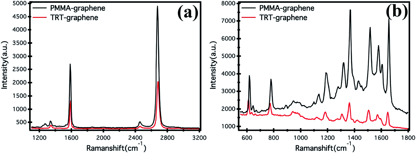 | ||
| Fig. 1 (a) Raman spectrum of TRT–graphene (red line), and PMMA–graphene (black line), (b) GERS effects of TRT–graphene (red), and PMMA–graphene (black). | ||
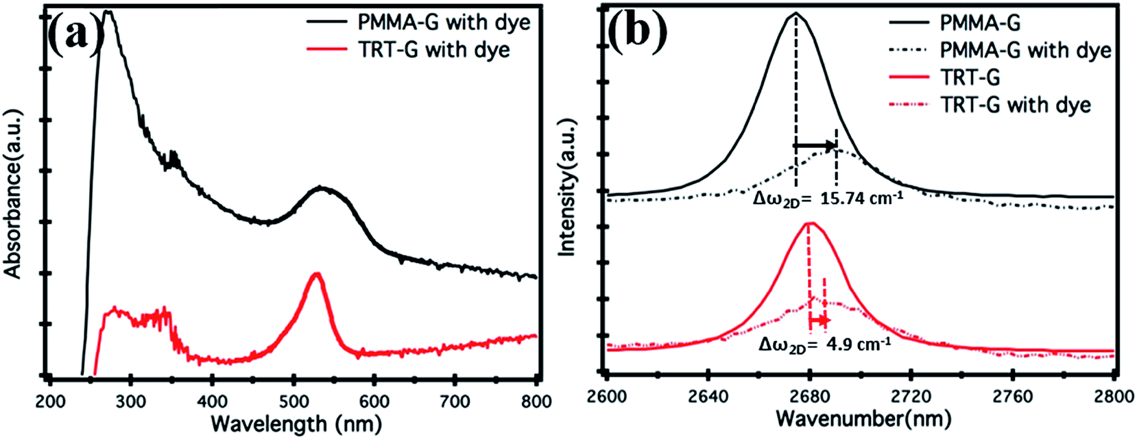 | ||
| Fig. 2 (a) UV-absorbance of R6G/PMMA–graphene/quartz (black) and R6G/TRT–graphene/quartz (red). (b) 2D peak of PMMA (black)– and TRT (red)–graphene before (solid) and after (dot) R6G adsorption. | ||
| G band (cm−1) | 2D band (cm−1) | |
|---|---|---|
| PMMA–graphene | 1587.03 | 2677.77 |
| TRT–graphene | 1590.74 | 2683.33 |
Fig. 2a shows the UV-absorbance results of R6G molecules on graphene prepared by the two transfer methods, with all other preparation parameters the same. The characteristic absorbance peak at 520 nm of the dye molecules on PMMA–graphene was much broader than for the TRT–graphene due to band splitting, implying transitions at both higher and lower energy induced by the formation of aggregated dyes.22 Furthermore, R6G/PMMA–graphene showed a higher contribution of C–C bonds at 265 nm than R6G/TRT–graphene, indicating that the π–π* interaction between PMMA–graphene and the probe molecules is stronger than for TRT–graphene.23Fig. 2b revealed another important difference in the Raman peaks. After adsorbing R6G dye on each graphene substrate, the Raman intensity was greatly reduced and the 2D position of both graphenes was upshifted compared to samples without the adsorbing dye. The 2D positions of PMMA– and TRT–graphenes were respectively upshifted by 15.74 cm−1 and 4.9 cm−1 compared to samples before dye deposition, implying PMMA–graphene had more hole-doping properties after dye adsorption. It has been reported that intensity weakening and a position shift of the 2D peak of graphene occur as a result of doping because electron–electron scattering becomes competitive with electron–phonon scattering.24 Therefore, the more significant hole doping properties in PMMA–graphene after dye adsorption are likely due to the larger amount of dye16 having much greater π–π* interaction and this may explain the higher GERS enhancement of R6G dye on PMMA–graphene.
In order to further explore the effects of molecular arrangements on charge transfer, the functional groups on the graphene surface were characterized by X-ray photoelectron spectroscopy. The detailed XPS results of PMMA– and TRT–graphene in Fig. 3, fitted using Casa XPS software, confirmed the presence of a large number of oxygen-containing groups such as C–O, COOH in both samples. In Fig. 3a, C–C, C–O and COOH in PMMA–graphene appeared with percentages of 59.85%, 27.90% and 12.25%, respectively. Fig. 3b denotes the XPS data of TRT–graphene with C–C, C–O and COOH percentages of 55.31%, 38.40% and 6.29%, respectively. COOH groups on the surface of PMMA–graphene are detected to have twice the concentration of those on TRT–graphene while the amount of epoxy/ether groups (C–O) is lower than for TRT–graphene. It can be inferred that either COOH or C–O on the surface of graphene affected the orientation of R6G and thus its π–π* interaction with the graphene surface.25 It has been reported that Coulombic interactions between the negatively charged COOH groups in GO and the positively charged R6G dye molecule26 allow firm binding between the substrate and the probe molecules.27 Furthermore, carboxyl groups, mainly located at the edges of the graphene surface do not interfere with the π–π* stacking of R6G dye molecules on the graphene surface. On the other hand, the epoxy/ether groups that reside on the planar surface of graphene tend to restrict π–π* interactions between the graphene surface and R6G. Consequently the R6G molecules are preferentially positioned at C–C sites on the surface of a graphene that has a larger amount of COOH groups and fewer C–O groups. The arrangement of R6G molecules on the surface of PMMA–graphene leads to strong π–π* interactions in the region where epoxy/ether groups are absent. As a result, the density of R6G molecules on the surface of PMMA–graphene was higher than on TRT–graphene, leading to a higher UV-absorbance peak intensity (Fig. 2a) and more hole-doping properties (Fig. 2b).
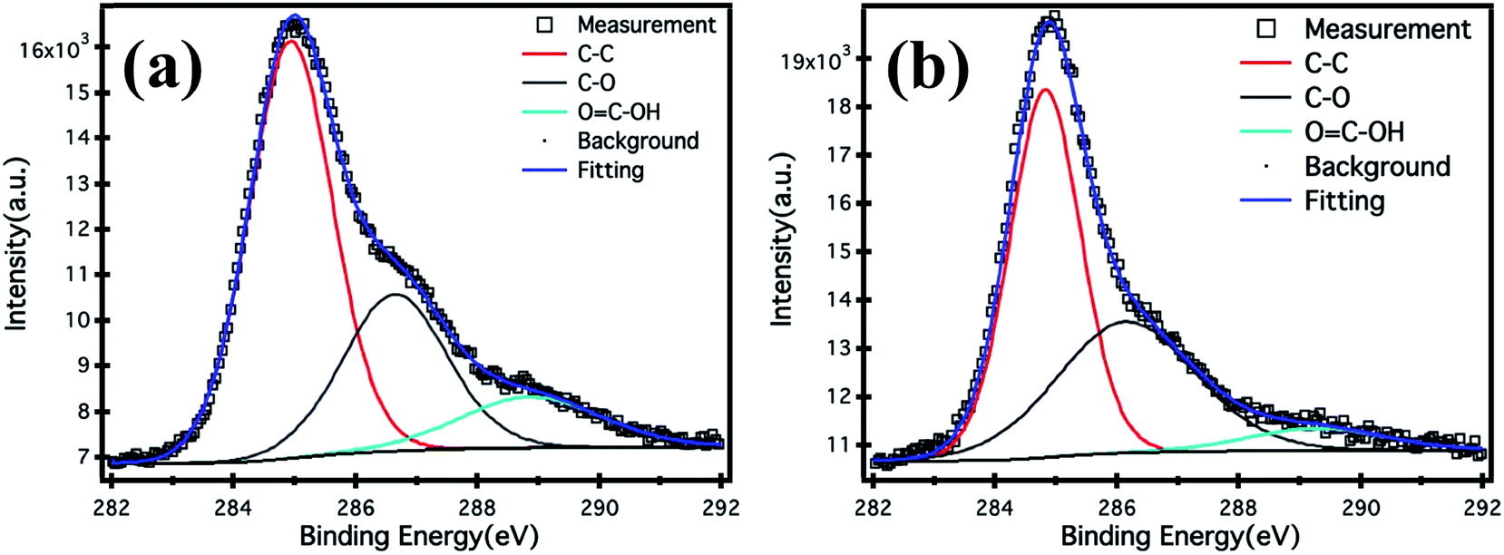 | ||
| Fig. 3 XPS data of (a) PMMA–graphene and (b) TRT–graphene. | ||
In order to confirm the greater GERS on PMMA–graphene, we have conducted fluorescence decay measurements of the samples using a fluorescence lifetime (FL) spectrometer (Edinburgh Instruments (Model number: FL920)) as shown in Fig. 4. The fluorescence decay time measurements give direct evidence of electron transfer between the dye and graphene. The fluorescence decay lifetimes of the samples were calculated using

 | ||
| Fig. 4 Fluorescence decay of R6G on a PMMA–graphene/quartz (cyan), TRT–graphene/quartz (blue), and quartz substrate (black line). | ||
The fluorescence lifetimes of R6G on PMMA–graphene/quartz, TRT–graphene/quartz, and quartz were calculated to be 0.234, 0.534, 2.44 ns, respectively (Fig. 4). R6G dye molecules on quartz showed the longest lifetime of 2.44 ns, which is slightly lower than the reported value of 3.8 ns, implying a lower concentration of dye molecules in the solution-based measurement conditions than in the substrate-based measurement ones. The one order of magnitude lower fluorescence lifetime of R6G on both the TRT-and PMMA-substrates compared to R6G indicates fast charge transfer between the dye and the graphene films, which supports the reason for the larger Raman scattering signals of R6G observed on the surface of graphene than on the SiO2/Si substrate. Importantly, the fluorescence lifetime for R6G/PMMA–graphene was half that for R6G/TRT–graphene, indicating the best charge transfer among the three samples. This is in good agreement with the 6 times greater GERS signal on PMMA–graphene than on TRT–graphene and bare quartz.
Conclusion
We have shown that PMMA–graphene has high GERS, up to 6 times that for the TRT–graphene, which can be attributed to the presence of strong π–π* interactions due to the presence of more COOH groups and fewer C–O groups in PMMA–graphene. The effects of the graphene transfer method on GERS are quite well explained by charge transfer properties between probe molecules and the graphene substrate. Our study clearly demonstrates the graphene transfer method and induced defects in graphene are important parameters in determining the magnitude of the GERS effect.Experimental procedure
Graphene growth and transfer process
Graphene growth on copper foil (Alfa Aeasr, 99.9999%) was performed by chemical vapor deposition (CVD) at 1000 °C. First 100sccm of H2 was passed over the foil while increasing the temperature to remove impurities on its surface. Then a continuous flow of 24 sccm of CH4 gas was passed through the quartz tube for 5 min, without turning off the H2, to grow the graphene. After growth, the temperature in the quartz tube rapidly decreased to room temperature. The graphene transfer processes were as follows. For PMMA–graphene, the graphene/Cu film was coated using a PMMA solution dissolved in toluene and then dried at 100 °C in an ambient air for 10 min. For the preparation of TRT–graphene, the tape was attached to the graphene/Cu film and pressure was then applied to remove air between the tape and sample. For both PMMA– and TRT–graphene, the Cu foil was removed from the sample by etching for 2 h in an ammonium persulfate solution. After removing the Cu foil, both samples were floated for 1 h on D.I. water to wash the etchant solution from the samples and dried using N2 gas. Finally the prepared sample was transferred onto the desired substrate.R6G dye adsorption on the graphene substrate
R6G as a probe molecule was dissolved in a DI water. The concentration of R6G in solution was 10−5 M (mol L−1). The molecule was adsorbed by soaking the sample in the prepared solution for 1 h followed by washing three times to remove any residue.GERS measurement
To confirm the GERS effects of the prepared substrate, combined AFM-Raman microscopy (WITec) was used to check the signal enhancement of R6G dye. R6G was dissolved in DI water with a concentration of 1 mM to obtain a stock solution and then diluted to obtain the required concentration. The substrate was dipped into the dye solution where it remained for 60 min to stabilize deposition. After adsorption, the substrate was rinsed by DI water. For the Raman measurements, the power was adjusted to 0.2 mW and integration time was set to be 10 s.Acknowledgements
We thank Prof. Rodney Ruoff and Prof. Peter Thrower for helpful discussion. This work was supported by IBS-R019-D1 and by NRF with contract no. NRF-2015-R1A2A2A01005250 and NRF-2012-R1A1A2043076.References
- (a) L. Gao, J. R. Guest and N. P. Guisinger, Epitaxial Graphene on Cu(111), Nano Lett., 2010, 10(9), 3512–3516 CrossRef CAS PubMed; (b) P. W. Sutter, J.-I. Flege and E. A. Sutter, Epitaxial graphene on ruthenium, Nat. Mater., 2008, 7(5), 406–411 CrossRef CAS PubMed.
- K. S. Novoselov, A. K. Geim, S. V. Morozov, D. Jiang, Y. Zhang, S. V. Dubonos, I. V. Grigorieva and A. A. Firsov, Electric field effect in atomically thin carbon films, Science, 2004, 306(5696), 666–669 CrossRef CAS PubMed.
- (a) S. Park and R. S. Ruoff, Chemical methods for the production of graphenes, Nat. Nanotechnol., 2009, 4(4), 217–224 CrossRef CAS PubMed; (b) W. S. Hummers Jr and R. E. Offeman, Preparation of Graphitic Oxide, J. Am. Chem. Soc., 1958, 80(6), 1339–1339 CrossRef.
- (a) X. Li, C. W. Magnuson, A. Venugopal, R. M. Tromp, J. B. Hannon, E. M. Vogel, L. Colombo and R. S. Ruoff, Large-Area Graphene Single Crystals Grown by Low-Pressure Chemical Vapor Deposition of Methane on Copper, J. Am. Chem. Soc., 2011, 133(9), 2816–2819 CrossRef CAS PubMed; (b) X. Li, W. Cai, J. An, S. Kim, J. Nah, D. Yang, R. Piner, A. Velamakanni, I. Jung, E. Tutuc, S. K. Banerjee, L. Colombo and R. S. Ruoff, Large-area synthesis of high-quality and uniform graphene films on copper foils, Science, 2009, 324(5932), 1312–1314 CrossRef CAS PubMed.
- J. Kang, D. Shin, S. Bae and B. H. Hong, Graphene transfer: key for applications, Nanoscale, 2012, 4(18), 5527–5537 RSC.
- W.-H. Lin, T.-H. Chen, J.-K. Chang, J.-I. Taur, Y.-Y. Lo, W.-L. Lee, C.-S. Chang, W.-B. Su and C.-I. Wu, A direct and polymer-free method for transferring graphene grown by chemical vapor deposition to any substrate, ACS Nano, 2014, 8(2), 1784–1791 CrossRef CAS PubMed.
- (a) Y. Wang, Y. Zheng, X. Xu, E. Dubuisson, Q. Bao, J. Lu and K. P. Loh, Electrochemical delamination of CVD-grown graphene film: toward the recyclable use of copper catalyst, ACS Nano, 2011, 5(12), 9927–9933 CrossRef CAS PubMed; (b) C. T. Cherian, F. Giustiniano, I. Martin Fernandez, H. Andersen, J. Balakrishnan and B. Özyilmaz, ‘Bubble-Free’ Electrochemical Delamination of CVD Graphene Films, Small, 2015, 11(2), 189–194 CrossRef CAS PubMed.
- (a) M. Fleischmann, P. J. Hendra and A. J. McQuillan, Raman spectra of pyridine adsorbed at a silver electrode, Chem. Phys. Lett., 1974, 26(2), 163–166 CrossRef CAS; (b) E. J. Blackie, E. C. le Ru and P. G. Etchegoin, Single-molecule surface-enhanced Raman spectroscopy of nonresonant molecules, J. Am. Chem. Soc., 2009, 131(40), 14466–14472 CrossRef CAS PubMed.
- P. L. Stiles, J. A. Dieringer, N. C. Shah and R. P. van Duyne, Surface-enhanced Raman spectroscopy, Annu. Rev. Anal. Chem., 2008, 1(1), 601–626 CrossRef CAS PubMed.
- (a) X. Ling, L. Xie, Y. Fang, H. Xu, H. Zhang, J. Kong, M. S. Dresselhaus, J. Zhang and Z. Liu, Can Graphene be used as a Substrate for Raman Enhancement?, Nano Lett., 2009, 10(2), 553–561 CrossRef PubMed; (b) F. Schedin, E. Lidorikis, A. Lombardo, V. G. Kravets, A. K. Geim, A. N. Grigorenko, K. S. Novoselov and A. C. Ferrari, Surface-Enhanced Raman Spectroscopy of Graphene, ACS Nano, 2010, 4(10), 5617–5626 CrossRef CAS PubMed.
- (a) X. Yu, H. Cai, W. Zhang, X. Li, N. Pan, Y. Luo, X. Wang and J. G. Hou, Tuning Chemical Enhancement of SERS by Controlling the Chemical Reduction of Graphene Oxide Nanosheets, ACS Nano, 2011, 5(2), 952–958 CrossRef CAS PubMed; (b) L. Zhang, C. Jiang and Z. Zhang, Graphene oxide embedded sandwich nanostructures for enhanced Raman readout and their applications in pesticide monitoring, Nanoscale, 2013, 5(9), 3773–3779 RSC.
- J. H. Lee, E. K. Lee, W. J. Joo, Y. Jang, B. S. Kim, J. Y. Lim, S. H. Choi, S. J. Ahn, J. R. Ahn, M. H. Park, C. W. Yang, B. L. Choi, S. W. Hwang and D. Whang, Wafer-scale growth of single-crystal monolayer graphene on reusable hydrogen-terminated germanium, Science, 2014, 344(6181), 286–289 CrossRef CAS PubMed.
- J. Liu, H. Cai, X. Yu, K. Zhang, X. Li, J. Li, N. Pan, Q. Shi, Y. Luo and X. Wang, Fabrication of Graphene Nanomesh and Improved Chemical Enhancement for Raman Spectroscopy, J. Phys. Chem. C, 2012, 116(29), 15741–15746 CAS.
- R. Lv, Q. Li, A. R. Botello-Mendez, T. Hayashi, B. Wang, A. Berkdemir, Q. Hao, A. L. Elias, R. Cruz-Silva, H. R. Gutierrez, Y. A. Kim, H. Muramatsu, J. Zhu, M. Endo, H. Terrones, J. C. Charlier, M. Pan and M. Terrones, Nitrogen-doped graphene: beyond single substitution and enhanced molecular sensing, Sci. Rep., 2012, 2, 586 Search PubMed.
- (a) X. Ling, J. Wu, L. Xie and J. Zhang, Graphene-Thickness-Dependent Graphene-Enhanced Raman Scattering, J. Phys. Chem. C, 2013, 117(5), 2369–2376 CrossRef CAS; (b) C.-C. Kuo and C.-H. Chen, Graphene thickness-controlled photocatalysis and surface enhanced Raman scattering, Nanoscale, 2014, 6(21), 12805–12813 RSC.
- R. Voggu, B. Das, C. S. Rout and C. N. R. Rao, Effects of charge transfer interaction of graphene with electron donor and acceptor molecules examined using Raman spectroscopy and cognate techniques, J. Phys.: Condens. Matter, 2008, 20(47), 472204 CrossRef.
- (a) C. S. Park, Y. Zhao, J.-H. Lee, D. Whang, Y. Shon, Y.-H. Song and C. J. Lee, Tunable bandgap of a single layer graphene doped by the manganese oxide using the electrochemical doping, Appl. Phys. Lett., 2013, 102(3), 032106 CrossRef; (b) H. Xu, L. Xie, H. Zhang and J. Zhang, Effect of Graphene Fermi Level on the Raman Scattering Intensity of Molecules on Graphene, ACS Nano, 2011, 5(7), 5338–5344 CrossRef CAS PubMed; (c) Q. Hao, S. M. Morton, B. Wang, Y. Zhao, L. Jensen and T. Jun Huang, Tuning surface-enhanced Raman scattering from graphene substrates using the electric field effect and chemical doping, Appl. Phys. Lett., 2013, 102(1), 011102 CrossRef PubMed.
- X. Ling, J. Wu, W. Xu and J. Zhang, Probing the Effect of Molecular Orientation on the Intensity of Chemical Enhancement Using Graphene-Enhanced Raman Spectroscopy, Small, 2012, 8(9), 1365–1372 CrossRef CAS PubMed.
- A. Pirkle, J. Chan, A. Venugopal, D. Hinojos, C. W. Magnuson, S. McDonnell, L. Colombo, E. M. Vogel, R. S. Ruoff and R. M. Wallace, The effect of chemical residues on the physical and electrical properties of chemical vapor deposited graphene transferred to SiO2, Appl. Phys. Lett., 2011, 99(12), 122108 CrossRef.
- Y.-C. Lin, C.-C. Lu, C.-H. Yeh, C. Jin, K. Suenaga and P.-W. Chiu, Graphene Annealing: How Clean Can It Be?, Nano Lett., 2011, 12(1), 414–419 CrossRef PubMed.
- H. Yang, H. Hu, Z. Ni, C. K. Poh, C. Cong, J. Lin and T. Yu, Comparison of surface-enhanced Raman scattering on graphene oxide, reduced graphene oxide and graphene surfaces, Carbon, 2013, 62, 422–429 CrossRef CAS.
- E. S. Thrall, A. C. Crowther, Z. Yu and L. E. Brus, R6G on graphene: high Raman detection sensitivity, yet decreased Raman cross-section, Nano Lett., 2012, 12(3), 1571–1577 CrossRef CAS PubMed.
- Y. Xu, H. Bai, G. Lu, C. Li and G. Shi, Flexible Graphene Films via the Filtration of Water-Soluble Noncovalent Functionalized Graphene Sheets, J. Am. Chem. Soc., 2008, 130(18), 5856–5857 CrossRef CAS PubMed.
- D. M. Basko, S. Piscanec and A. C. Ferrari, Electron–electron interactions and doping dependence of the two-phonon Raman intensity in graphene, Phys. Rev. B: Condens. Matter Mater. Phys., 2009, 80(16), 165413 CrossRef.
- J. Balapanuru, J.-X. Yang, S. Xiao, Q. Bao, M. Jahan, L. Polavarapu, J. Wei, Q.-H. Xu and K. P. Loh, A graphene oxide–organic dye ionic complex with DNA-sensing and optical-limiting properties, Angew. Chem., Int. Ed., 2010, 49(37), 6549–6553 CrossRef CAS PubMed.
- (a) N. Mohanty and V. Berry, Graphene-Based Single-Bacterium Resolution Biodevice and DNA Transistor: Interfacing Graphene Derivatives with Nanoscale and Microscale Biocomponents, Nano Lett., 2008, 8(12), 4469–4476 CrossRef CAS PubMed; (b) X. Wang, S. Zhong, Y. He and G. Song, A graphene oxide–rhodamine 6G nanocomposite as turn-on fluorescence probe for selective detection of DNA, Anal. Methods, 2012, 4(2), 360–362 RSC.
- (a) Y. Liang, D. Wu, X. Feng and K. Müllen, Dispersion of Graphene Sheets in Organic Solvent Supported by Ionic Interactions, Adv. Mater., 2009, 21(17), 1679–1683 CrossRef CAS; (b) H. Ren, D. D. Kulkarni, R. Kodiyath, W. Xu, I. Choi and V. V. Tsukruk, Competitive Adsorption of Dopamine and Rhodamine 6G on the Surface of Graphene Oxide, ACS Appl. Mater. Interfaces, 2014, 6(4), 2459–2470 CrossRef CAS PubMed.
Footnote |
| † Electronic supplementary information (ESI) available. See DOI: 10.1039/c5ra11100e |
| This journal is © The Royal Society of Chemistry 2015 |