DOI:
10.1039/C5RA10837C
(Paper)
RSC Adv., 2015,
5, 76092-76100
Direct-writing of circuit interconnects on cellulose paper using ultra-long, silver nanowires based conducting ink†
Received
8th June 2015
, Accepted 1st September 2015
First published on 1st September 2015
Abstract
A highly stable conducting nanoink based on silver ultra-long nanowires (Ag ULNWs) was developed by a self-seeding polyol method with controlled doping of silver acetate for flexible electronics applications. Ionic diffusion followed by the reduction of Ag+ ions was found to have a significant role on the network conductivity by reducing the contact resistance of the conducting patterns. Crack-free, bendable conductive patterns could be produced by a direct-writing approach with superior conductivity. The electrical properties of the nanowire ink patterns have been analysed with respect to pattern length, time and temperature. A two dimensional (2D) rectangular resistive network model has been adopted to depict the role of network density, percolation density and contact resistance of these conducting nanowire networks. Further, various electronic arts and circuit interconnects were drawn on cellulose paper substrates using a direct-writing approach and their performances have been successfully manifested.
Introduction
Flexible electronics using metal nanoparticles have an immense impact in various fields such as, wiring, displays, photovoltaics, RFIDs, sensors, transistors and antennas.1–13 In order to realize these applications, several materials have been developed to fulfil the needs of flexible electronics in the form of conducting inks based on conducting polymers, organometallic compounds, metallic precursors, and metallic nanostructures.14–22 The conducting polymer based inks showed much lesser conductivity compared to that of metals. Whereas, organometallic/metal based components have exhibited better electrical conductivity than conducting polymers after post-heat treatment process. But, these materials eventually degrade and affect the performance of the host electronic devices. To overcome such issues, intensive studies are going on to develop stable metallic nanoinks, due to their unique electrical, thermal and mechanical properties. Last few years, numerous research works based on silver nanoparticles have been reported in the field of printed electronics.23–25 The silver nanowires showed much higher electrical conductivity and better chemical stability than PEDOTs, CNTs, Cu and Al based nanoinks.26,27 Especially, silver nanowires forms reticular structures which tolerate significant strains because of their superior mechanical properties.28,29 In addition to these properties, conducting ink must be stable at room temperature for several months without any phase changes. The silver nanowires could be synthesized by well-established methods, like, polyol process,30–33 solvothermal,34 microwave-assisted route,35 wet-chemical,36,37 air-assisted synthesis,38 and hydrothermal methods.39,40 Any conducting patterns can be drawn on flexible substrates using aerosol-jet printing,27 inkjet printing,5,7,41 lithography technology,14 gravure printing,42 flexography.43 Still there are few complications existing in development of high quality conducting inks for implementing them in flexible electronics applications, such as, (i) fluidic instability of pattern; (ii) crack formation in printed patterns during post-treatment (iii) creating the scalable high-resolution patterns and (iv) adhesion and mechanical strength of the printed patterns on flexible substrates (PET, PDMS, Kapton, photo paper, etc.).44–49 Extensive research have been carried out to explore the potential of “paper electronics” by developing many proof-of-concept electronic components.50 The paper based substrates are commonly available, cost effective, environment friendly, recyclable, lightweight and can be tailor made into any 3D configurations.10,51–53 Among various printing techniques, direct-writing approach is a simple and cost-effective method for constructing desired conductive patterns on paper based substrates for various flexible electronics applications by a single-step process. To draw such hybrid printed paper electronics circuits on paper substrates, it is necessary to make low resistance electrical interconnects between the conductive components. In conventional printed circuit boards, the resistance of the printed conducting tracks could contribute more towards the total resistance of the system. This can contribute additional power dissipation which could be more challenging in case of battery operated system. Till date very few investigations have been carried out on paper-based interconnects using conventional silver nanoinks.54
In the present investigation, highly stable conducting nanoink based on silver ultra-long nanowire (Ag ULNWs) was developed by self-seeding polyol method with controlled doping of silver acetate. This was found to play a major role in decreasing the contact resistance of the nanowire network by ionic diffusion followed by reduction processes. Crack-free, bendable conductive patterns could be produced by direct-writing approach with superior conductivity. A 2D rectangular resistive network model was adopted to depict the role of network density, percolation density and contact resistance on conducting nanowire network. Conductive texts, electronic art works, circuit interconnects for standard surface mount device (SMD) components (e.g. light emitting diodes (LEDs)) and through-hole components were successfully portrayed on paper substrates and demonstrated using conductive silver ultra-long nanowire (Ag ULNW) ink.
Experimental details
Materials
Silver nitrate (AgNO3, 99.8%, SD Fine), hydroxyethyl cellulose (HEC, SD Fine Chemicals), methanol (99.8%, SD Fine Chemicals), ethylene glycol (EG, 99%, Merck), methanol (CH3OH, 99%, Merck), poly(vinyl-pyrrolidone) (PVP, MW: ∼40![[thin space (1/6-em)]](https://www.rsc.org/images/entities/char_2009.gif) 000, 99%, Himedia), silver acetate (CH3COOAg, 98%, Himedia) silver chloride (AgCl, 99%, Himedia) were used for Ag ULNWs synthesis and conducting nanoink preparation. All chemicals used for synthesis were of analytical grade and used without further purification. All solutions were prepared using ultra-pure water (Merck-Millipore, resistivity ≈ 18.2 MΩ cm).
000, 99%, Himedia), silver acetate (CH3COOAg, 98%, Himedia) silver chloride (AgCl, 99%, Himedia) were used for Ag ULNWs synthesis and conducting nanoink preparation. All chemicals used for synthesis were of analytical grade and used without further purification. All solutions were prepared using ultra-pure water (Merck-Millipore, resistivity ≈ 18.2 MΩ cm).
Preparation of ultra-long silver nanowires (ULNWs)
To synthesize ultra-long nanowires, polyol method was adopted.32,38 Briefly, 40 mL of EG was used as reducing agent and 0.67 g of PVP as structure-directing agent, by maintaining the reaction temperature at 180 °C. For the initial nucleation of silver seeds, 0.05 g of AgCl was added to the above mixture. The solution colour was changed from colourless to pale yellow. Further, actual silver source, 0.22 g of AgNO3 was added to this blend. The reaction was continued at constant temperature (180 °C) for 30 min. At the end of the reaction, the pale yellow colour of the solution was transformed to a greyish green. Immediately, the solution was quenched at room temperature. Further, methanol was added to the PVP functionalized silver nanowires to induce rapid coagulation. Later, the solution was transferred into a vial for centrifugation to remove excess PVP and EG. The precipitate was re-dispersed in 30 mL of CH3OH.33 Vacuum filtration was carried out to remove the by-products formed along with silver nanowires.
Nanowire ink preparation
The Ag ULNWs based conducting nanoink was developed by dispersing silver nanowires in methanol. To adjust the viscosity of the nanoink, viscosifying agent, HEC was used. The viscosifying solution was prepared by dissolving 4 wt% of HEC in a binary mixture of water and methanol (1:1 ratio), and stirred at 70 °C until a transparent liquid was observed. The nanoink rheology was tailored by adding the viscosifier, HEC (aliquots of 1 mL), to 30 mL of Ag ULNWs solution dispersed in CH3OH. Further, 400 μL of 0.1 M silver acetate solution was added to the nanoink, which increased the silver content of the Ag ULNWs ink solution. The measured apparent viscosity of the Ag ULNW ink was 2.5 cP which contained 3 wt% of Ag ULNWs. Further, ink was filled in a roller-ball gel pen for drawing the desired pattern on the cellulose paper substrate by direct-writing approach.
Characterization techniques
The optical properties of silver nanowires were analysed using T90+ UV-Visible spectrophotometer (PG Instruments, UK). The microstructure of Ag ULNWs was characterized by Atomic Force Microscopy (NTEGRA-AURA, NTMDT, Russia) and High Resolution Transmission Electron Microscopy (JEOL JEM-2010, Japan). The transmission electron microscopy (TEM) images of Ag ULNWs were acquired at 200 kV with an energy dispersive spectrometer. The viscosity of the nanoink solution was measured by a viscometer (DV-E, Brook field Engineering Laboratories, Inc. USA) at room temperature. A spindle with rotational speed of 60 rpm was used to compute the viscosity of the Ag ULNWs based nanoink. The texture of Ag ULNWs nanoink was observed using polarized optical light microscopy (Carl Zeiss Axioscope, Germany). The resistance of the ink and current–voltage (I–V) characteristics of Ag ULNW ink was measured by electrometer (Keithely, model-SMU-2420, USA).
Results and discussion
The Ag ULNWs were synthesized by polyol reduction.32 During this reaction, AgNO3 was reduced in the presence of Ag seeds and EG, to form Ag nanoparticles through heterogeneous and homogeneous nucleation processes. In the presence of Cl− and dissolved O2, both rapid crystal growth and oxidative etching were found to occur competitively.38 Subsequently, rate of growth in the various facets of Ag can be controlled in the presence of structure directing agent, PVP molecules.32 Fig. 1, shows synthesis process adopted for Ag ULNWs nanoink preparation. The silver nanowires were found to have an average diameter of 65 nm and length up to 7 μm. The obtained Ag ULNWs were re-dispersed in methanol and viscosifier with controlled addition of silver acetate. Addition of Ag+ ions (i.e. silver acetate) assists the formation of NW–NW junctions in the nanowire network during solvent evaporation. This can be attributed to the diffusion of silver ions towards the weakly populated PVP encapsulation at the NW junctions followed by reduction process. This can in turn decrease the junction/contact resistance of the adjacent NWs present in the Ag ULNWs network and improve the conductivity. The formation pathway of conducting bridges in NW network is depicted in Fig. 2.
 |
| | Fig. 1 Schematic illustration of seed-mediated ULNW growth mechanism and conducting ink preparation process. | |
 |
| | Fig. 2 Schematic representation of role of silver acetate in the formation of conducting pathways in complex nanowire network. | |
When silver nanowires absorbs light, conduction band electrons on the surface of nanowires undergo polarization due to the electromagnetic nature of light and exhibits the characteristic surface plasmon oscillations.55 The variation in the dimensions of silver nanostructures can be highly reflected on their absorption spectra. Fig. 3 illustrates absorption spectrum of silver nanowires dispersed in methanol. The spectrum exhibited two relatively sharp surface plasmon resonance (SPR) peaks at 351 and 378 nm positions. Generally, these two SPR peaks are attributed to the quadrupole resonance excitation and the transverse plasmon resonance of the Ag ULNWs with pentagonal cross-section30,50,56 (Fig. 3 inset). If the dimension of the nanowires is larger than the wavelength of the light, the free electrons are getting excited and travel along the growth axis. However, the amplitude of the electromagnetic waves (Eo) is uneven throughout the nanowire structure.
 |
| | Fig. 3 UV-Vis absorption spectrum of Ag ULNWs solution (inset shows the photograph of Ag ULNW solution) and (inset: schematic illustration of plasmonic nanowires as excited by the electric field Eo of incident light with wave vector k). | |
Fig. 4(a–c) shows the TEM images of Ag ULNWs synthesized by self-seeding polyol process. Initially, silver seeds were found to be nucleated in the form of 5-fold twinned Ag nanostructures which acted as seeds for subsequent growth of silver nanowires. Formation and growth of Ag ULNWs may be driven by the deposition of silver atoms on {111} planes of these 5-fold twinned nanostructures. The presence of PVP on Ag {100} plane of 5-fold twinned nanostructures could be a reason for the one dimensional growth along the longitudinal axis of Ag ULNW. Also, the PVP molecules could benefit the formation of silver nanowires by strongly attaching to the Ag {100} and {110} rather than {111} facets.30,31 The density of PVP molecules bound to the side surfaces of the nanowires is very high compared to that of edges of the Ag ULNWs, which permits growth along the nanorods axis leading to high aspect ratio nanowires. The analysis also reveals the end-to-end and junction-to-junction contacts between the nanowires which can facilitate free conduction pathways for the transport of electrons throughout the nanorods network. V-shaped nanowires were found to be formed with different bending angles as observed from HR-TEM images shown in Fig. 4(a–c). The minimization of surface energy happens through lattice match between the adjacent nanowires. It enables the fusion growth, and twinned crystal plane-induced growth of the V-shaped Ag nanostructures.31 Apparently, a thin amorphous layer was start to be formed over silver nanowire surface, which may be due to the strong attachment of PVP molecules. The SAED pattern was recorded from the junctions is shown in the inset of Fig. 4d. Two or more sets of diffraction spots were observed, corresponding to the {111}, {200}, {220}, {311}, and {222} planes of silver. The V-shaped nanowire exhibited different twisting angles (e.g., ∼90°, ∼120°, ∼150°). Similar observation was reported by Liu et al., and Gao et al., on the twisting angles in the range of 110–150° and 90–170° of silver nanowires respectively.57,58 In V-shaped nanowire, the twinning area of two adjacent nanowires are fused by {111} facets to form a ultra-long bended nanowire structure. The formation of such elongated nanostructures is probably caused by sharing a twinned crystal plane. Zhang et al., stated that the matching of {111} facet makes the binding between two 5-fold twinned nuclei and grow independently as a nanowire.59 TEM and atomic force microscopy (AFM) analyses confirmed the 1D growth of silver nanorods to nanowires as depicted in Fig. 5(a and b) and (c and d) respectively. It is evident that the Ag ULNWs were found to have an average diameter of ∼65 nm and length of about ∼7 μm. These high aspect ratio nanowires fused to the adjacent wires to form ultra-long nanowires due to the smaller density of PVP molecules at the ends.
 |
| | Fig. 4 (a–c) HR-TEM images of V-shaped Ag ULNWs (inset: magnified image of V-shaped portion) and (d) SAED pattern of Ag ULNWs. | |
 |
| | Fig. 5 (a and b) HR-TEM images (inset: particle size distribution profile) and (c and d) AFM images of the Ag ULNWs. | |
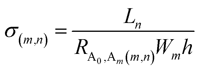
Electrical characterisation was carried out to comprehend the transport properties of the nanowire network using current–voltage (I–V) measurements using two-probe method. If the diameter (DNW) of nanowire is relatively smaller than electron mean free path, the electrical resistivity (ρNW) of the nanowire increases.60 Effective resistance of the uniform metal nanowires is always higher than the bulk due to surface scattering. Maximum current density supported by the nanostructure depends on the cross section area.61 When number of nanowires (NWs) per unit area decreases, the nanowire network may fail to form a conducting pathway across the network. At a critical nanowire number density (NC) (i.e. percolation threshold) continuous conducting channels will be formed through the interconnected NWs. The nanowire length (LNW) and critical nanowire number density (NC) are inversely proportional to each other as shown in eqn (1),53,62
| |
 | (1) |
High aspect ratio NWs generally possesses low NC. The eqn (1) is valid only for larger patterns, whereas the pattern size to LNW ratio is larger than 30.63 In the present investigation, conducting nanowire network was formed by ultra-long Ag ULNWs (LNW: ∼7 μm length). The model developed by Mutiso et al., was adopted for the 2D random nanowire networks to understand the percolation dependence of electrical properties of the conducting nanowire patterns.67
The thickness of the pattern was found to be in nanometer range (∼500 nm) which is comparatively far less than the dimension of width and length of the pattern. So, Ag ULNW network was assumed as a 2D network and Z axis term thickness was considered as negligible. However, in both 2D and 3D conducting network models, the percolation theory predicts the power-law dependence electrical conductivity (σ) of a network of conducting particles as,
| |
 | (2) |
where, critical nanowire number density (
NC) and number of nanowires per unit area (
N) values are calculated from the experimental findings and critical component ‘
t’ was fixed as 1.3 for 2D percolation and 2 for 3D percolation.
64–66,80 It is possible to use the percolation relation for measuring the conductivity (
σ) in such network structures using
eqn (2).
80 It is evident that higher
N value leads to low
Rs. In order to make maximum number of interconnections in the network, it is necessary to maximize the aspect ratio of the NWs. However, the conducting patterns drawn on paper substrate contains high aspect ratio (
LNW/
DNW) Ag ULNWs and hence the percolation probability has to be increased which creates conducting channel across the network with lower
NC and higher
N values. The Ag ULNWs allow electrons to propagate larger distance through the nanowires without facing contact resistance owing to their high aspect ratio. In such nanowire networks, contact resistance (
Rc) plays a crucial role in electron propagation. As per
eqn (2), it is evident that
Rc depends on
N and
NC. The value of
Rc between the NWs is always higher than that of individual nanowire resistance (
Rwire). Assuming conducting nanowires forming
n ×
n square network with zero
Rc. As per Kirchhoff's rule,
Rs for a square network is defined in
eqn (3) and
(4).
23| |
 | (3) |
| |
 | (4) |
where
ρ is the resistivity of the NW,
l is the length of the wire,
w is the wire width, and
h is the height of the wire. Ratio of
N/(
N + 1) approach unity for network with larger
N value. Finally,
Rs is approximately equal to
ρl/
wh. In the present investigation, the conducting line pattern was considered as 2D rectangular resistive network, which consist of
m ×
n grid as shown in
Fig. 6. Here, the unit resistance and grid number of the rectangular resistor network in both horizontal and vertical directions are denoted by
r,
r0 and
n,
m respectively. The equivalent resistance (
i.e. RA0,Am(m,n)) between two nodes A
0 and A
m in such finite rectangular network system was calculated using auxiliary function
F(
m,
n) by Tan
et al.68 In 2D resistive Ag ULNW network, assuming
r =
r0 =
Rwire, and contact resistance
Rc, the modified sheet resistance of the network can be defined by,
| | |
RA0,Am(m,n) ≈ Rs ≈ Rwire[F(m,n)] + Rc(i,j)
| (5) |
where,
Rc(
i,
j) is the total contact resistance existing in a 2D network. Here,
Rc(
i,
j) of the rectangular resistor network arise due to presence of NW contact in both horizontal and vertical directions are denoted by
i,
j respectively. The value of auxiliary function
F(
m,
n) depends on
m and
n values. The values of
m and
n are difficult to find from experiments. We cannot neglect the term
F(
m,
n) in the
eqn (5). During solvent evaporation, adjacent silver nanowires could be welded at the nanowire junctions and
Rc(
i,
j) could be minimized,
67 which are manifested in the TEM images of Ag ULNWs. Assuming the network is a solid conducting line with zero
Rc(
i,
j), the nanowire network resistance
RA0,Am(m,n) is approximately equal to
Rs for larger networks. From
eqn (4) and
(5), the conductivity (
σ(m,n)) of the Ag ULNWs network can be calculated from the following equation,
80| |
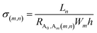 | (6) |
where,
Ln is a length of the pattern/network which contains
n number of NWs, and
Wm is a width of the pattern/network which contains
m number of NWs. Conductivity (
σ(m,n)) of the network was directly related with
N and
NC.
67 The value of
RA0,Am(m,n) can be directly measured from the
I–
V characteristics. Upon applying a constant direct current to opposing nanowires, the junction region get melted locally and fuse together due to current-induced heating (Joule heating).
69 This can alter the contact resistance between nanowires. To avoid this phenomenon, maximum of ±0.5 V was applied to the pattern during
I–
V measurement. For calculating the conductivity (
σ(m,n)) of the network, it was assumed that the patterns were having uniform thickness (
t) throughout their length. From
eqn (6), the conductivity of bare Ag ULNW ink based pattern was found to be 0.36 × 10
5 S cm
−1 and their equivalent resistance was calculated as 2.7 Ω (see
Fig. 7a). Further, electrical behaviour of the conducting patterns were analysed. The
I–
V characteristics reveals that the addition of Ag
+ ions significantly reduces the network resistance to ∼678 mΩ (
σ(m,n) ≈ 1.48 × 10
5 S cm
−1). The enhancement in conductivity could be related to NWs junction formation. The
I–
V characteristic curves corresponding to the patterns drawn on the paper substrate with varied lengths are shown in
Fig. 7b. It was observed that shorter lengths exhibited very small resistance (1 cm and 2 cm), and as length increased the line resistance was found to be increased (3, 4 and 5 cm). The conductivity of the smallest conducting line (
i.e. L = 10 mm,
W = 2 mm and
t ≈ 500 nm) was calculated as ∼1.48 × 10
5 S cm
−1. The corresponding
NC value was found to be ∼8000 wires, which depends on the length
L. The value of
N was obtained from
eqn (2) and calculated to be 76 × 10
6. The critical component ‘
t’ was considered to be 1.3 for 2D NW network. For 3D NW network, the
N value become 3.1 × 10
6, and
t was 3 expected for 3D percolation. However,
N was much greater than the
NC in both 2D and 3D network. Under this condition, increased electrical conductivity could be aroused from formation of more percolated pathways due to random network formation, whereas at higher degrees of orientation, the conducting pathways are ultimately demolished, resulting in a loss of electrical conductivity.
70 The calculated conductivity value of the Ag ULNW nanoink was comparable with recently reported value (∼10
5 S cm
−1).
71,72 From the calculated values, it was evident that the auxiliary function
F(
m,
n) and
Rc(
i,
j) are playing significant role for determining the random nanowire network resistance. For comparison, the operating parameters of the silver based conducting inks have been summarized in Table S1 (ESI
†). The conductivity of the pattern was analysed with respect to length as depicted in
Fig. 7b inset. It was observed that the decrease in conductivity with respect to length. In general,
σ(m,n) is constant throughout the length. But during direct writing technique, it is difficult to maintain the uniform thickness throughout the pattern. This can influences the network density at every point in the conducting pattern. Hence, it is not due to the intrinsic property of the material and it originates from geometry of the pattern especially from
N value.
73 The value of
R(A0,Am(m,n)) increases with
Ln, increases the network contact resistance (
Rc(i,j)), which results in decrease in conductivity (
σ(m,n)) as per
eqn (6). Also, density of the nanowires (
N) is depends on the geometry of the pattern. When
N ≪
NC, it significantly influences the conductivity of the pattern.
 |
| | Fig. 6 Rectangular resistive network with m × n grid. | |
 |
| | Fig. 7 Current–voltage (I–V) characteristics of (a) drawn pattern (1 cm length) using conducting ink with/without silver acetate, (b) drawn patterns with various lengths using silver acetate incorporated conducting ink (inset: conductivity vs. pattern length). | |
The conducting pattern drawn by Ag ULNW ink was showing more conductivity than Ag+ ion free ink. The surface of the Ag ULNWs are weakly wrapped with PVP through the coordination of the nitrogen atom (N) in PVP, imparting steric effect.74 TEM images showed that a uniform thin layer of PVP with 1–3 nm thickness present on the Ag ULNW surfaces (Fig. S1 in ESI†). As mentioned in earlier discussion, the weakly adsorbed PVP can readily collapse after solvent evaporation on the surface of NW forming nanowire junctions. The Ag ULNWs further tend to self-aggregate to form conductive films.75 The Ag+ ions available due to silver acetate doping in the Ag ULNW ink therefore can migrate into the junction of the adjacent nanowires during solvent evaporation. Presence of more accessible metal surface at the Ag ULNWs junctions due to lower population of PVP molecules improves the tendency of Ag+ ions to migrate and get reduced at the junctions further soldering the nanowires to form nanowire network76 (see Fig. 2). However, the obtained conductivity value was found to be ∼4.2 times lower than the bulk conductivity of Ag (6.3 × 10⁵ S cm−1). The length of Ag nanowires used in conducting ink is about 7 μm, which is extremely larger than the mean free path of electrons (λ ≈ 30 nm for silver), so resistance of the individual nanowire can be significant, which may influence the NW conductivity.77
Further, the electrical resistance of the drawn pattern was analysed as a function of time and temperature. The resistance was found to be decreasing as a function of time (as depicted in Fig. 8) and reached up to ∼50 Ω at room temperature. The initial decrease in resistance may be due to the fast evaporation of solvent molecules present over the nanowire network (indicated in arrow 1). The slow decay of network resistance is because of the slow evaporation kinetics of the trapped solvent molecules inside the complex nanowire network (indicated in arrow 2 and 3). This process continued until it reached the saturation level. The solvent evaporation can be accelerated by heat treatment. Russo et al., observed higher electrical conductivity (2.26 × 10⁵ S cm−1) of the silver nanoparticles based ink at higher temperatures (≥170 °C) and low electrical conductivity (0.5 × 10⁴ S cm−1) at room temperature, which is ascribed to residual solvent present in the printed pattern.78 The effect of processing temperature on the network resistance was studied as shown in inset of Fig. 8. The resistance of the pattern was found to be decreased as a function of temperature. This negative trend may be owing to the fusion of adjacent nanowires due the presence of Ag+ ions at the ohmic junctions and also from evaporation of residual solvent molecules present in the network. As the temperature reaches about 150 °C (i.e. glass transition temperature of PVP), the thin shell of residual PVP molecules (Fig. S1 in ESI†) on the Ag ULNWs surface starts to flow and making more contacts/junctions between adjacent Ag ULNWs. Above 150 °C, the residual layer of PVP molecules start undergoing thermal degradation.79 This phenomenon further decreases the total contact resistance Rc(i,j) of the network. Thus, the electrical characterization and 2D network analysis could clearly elucidate the role of Ag+ ions, NWs network density (N) and contact resistance on Ag ULNWs network conductivity.
 |
| | Fig. 8 Aging profile of the conducting ink as a function of solvent evaporation time (inset: resistance vs. temperature). | |
 |
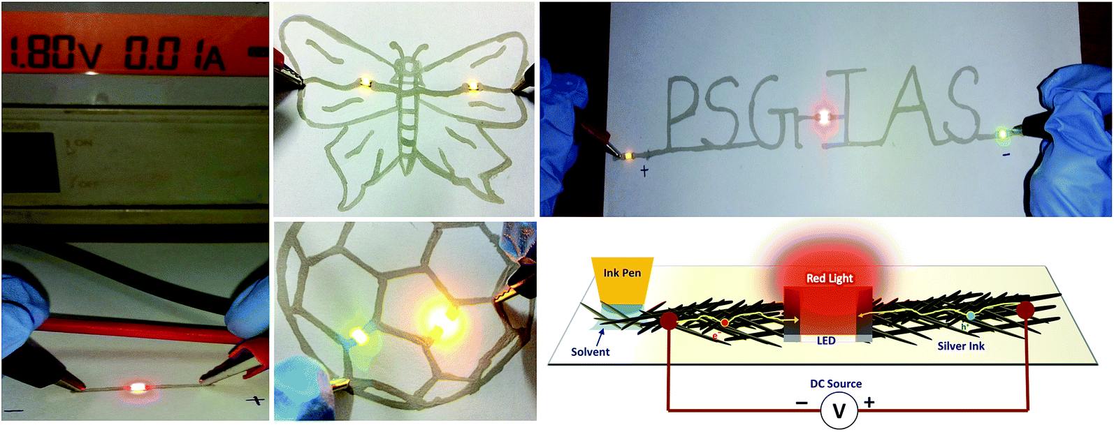
| | Fig. 9 Polarized microscopic image of conducting line pattern in (a) flat position (b) bend position and photographs of the pattern in (c) flat and (d) bent states (inset: LED demonstration at flat and bend state. The LED remains “ON” during the bending process, showing that the electrodes remain conductive during deformation). | |
Further, the mechanical flexibility of the Ag ULNWs nanoink line pattern was investigated by repeatable bending cycles. No crack formation or delamination was observed in polarized microscopic image analysis (as shown in Fig. 9). This may be due to the excellent adhesion between the ink and cellulose fiber networks. The presence of Ag+ ions in the ultra-long nanowire inks can improve the electrical properties of the patterns. Moreover, the nanoink can be stored under ambient conditions for a longer period. It is likely to expand the applications of Ag ULNWs conducting ink in complex, flexible electronics. To establish the utility of Ag ULNWs ink for paper electronics applications, cellulose paper was chosen as a substrate for drawing electronic arts using the Ag ULNWs based conducting ink. Whereas, in conventional flexible electronics, un-friendly raw materials, such as epoxy resin, glass fibers, and copper foils have been used. The Ag ULNW ink was used to make an electrical interconnects for the simple “potential divider” circuitry by direct-writing method. In potential divider circuit, specific combinations of resistors (R1 and R2) are used to “divide” the voltage into precise proportions with respect to R1 and R2 ratio. The potential divider circuit and its corresponding outputs are shown in Fig. 10. Before fabrication of the potential divider circuit, the same circuit was simulated with the help of LT Spice software. The simulated results are shown in the inset of Fig. 10. The output voltage of potential divider can be calculated as,
| |
 | (7) |
where,
Vo is the output voltage,
Vin is the input voltage and
R1 and
R2 are resistance of the two resistive arms. For this circuit,
VDC = 5.01 V was used as an input voltage and two 1 kΩ resistors were used as a divider. The divider ratio was kept as 0.5. The output voltage of 2.56 V was measured by the Digital Multimeter (DMM) as shown in
Fig. 10. The deviation (
i.e. 0.06 V) in the output is due to tolerance of the resistors,
R1 and
R2.
 |
| | Fig. 10 Photograph of the potential divider circuit drawn using Ag ULNWs ink (inset: corresponding circuit and simulation result). | |
 |
| | Fig. 11 Photographs of electronic arts drawn on the paper substrate using Ag ULNWs nanoinks and schematic representation of electronic conduction through nanowire network during LED demonstration. | |
Also, the applications of Ag ULNW nanoinks inflexible electronics were extended with demonstration of various conducting arts on paper substrates. The surface mount colour LEDs were used to demonstrate with various conducting arts on the paper substrates. The surface mount colour LEDs were used to demonstrate large area electronic art works to show a conductivity of the arts. Minimum voltage of 1.8 V was applied for biasing the LEDs and the schematic representation of electronic transport through the nanowire network during LED demonstration also depicted in Fig. 11. Finally, the paper based E-arts and electronic circuits are more environmentally friendly due to flexible nature; whereas epoxy requires a high temperature of 800 °C to decompose, and emit toxic gases. The eco-friendly highly conductive Ag+ ion embedded Ag ULNWs ink prepared from polyol process show the great advantages of paper based electronic circuits which will provide to the trend of eco-friendly products and sustainability of future electronics.
Conclusion
To summarize, silver ultra-long nanowire (Ag ULNWs) based conducting nanoink was successfully developed using self-seeding polyol method by controlled doping of silver acetate. The Ag+ ion incorporated nanowire ink was highly stable and showed excellent conductivity about 1.48 × 10⁵ S cm−1 than ion free ink. Ionic diffusion followed by the reduction of Ag+ ion was influence the network conductivity by reducing the junction (contact) resistance of the conducting patterns drawn by direct-writing approach. A 2D rectangular resistive network model was clearly depict the role of network density (N), percolation density (NC) and contact resistance on conducting nanowire network. It is possible to maintain the uniform conductivity throughout the length, by maintaining the parameter N and NC. However, N was much greater than the NC in both 2D and 3D network. This could be from formation of more percolated pathways due to random network formation. Further, various electronic art work and circuit interconnects were demonstrated on paper substrates by the direct writing approach. We hope Ag+ ion integrated ultra-long silver nanowire ink will be useful for making electronic interconnects on paper substrate using direct-writing approach for future paper based electrical interconnects for photovoltaic, sensors and flexible electronics applications.
Acknowledgements
Authors wish to acknowledge the facilities and support provided by the management, PSG Sons and Charities, Coimbatore. The author DJ acknowledges CSIR, New Delhi, INDIA for fellowship. Authors acknowledge Mr K. K. Karthikeyan, Research Assistant, PSG Institute of Advanced Studies, Coimbatore for AFM analysis.
References
- W. S. Wong and A. Salleo, Flexible electronics: materials and applications, Springer Science & Business Media, 2009 Search PubMed.
- A. Kamyshny, J. Steinke and S. Magdassi, Open Appl. Phys. J., 2011, 4, 19–36 CrossRef CAS.
- S. Jeong, H. C. Song, W. W. Lee, S. S. Lee, Y. Choi, W. Son, E. D. Kim, C. H. Paik, S. H. Oh and B.-H. Ryu, Langmuir, 2011, 27, 3144–3149 CrossRef CAS PubMed.
- B. Comiskey, J. D. Albert, H. Yoshizawa and J. Jacobson, Nature, 1998, 394, 253–255 CrossRef CAS.
- C. N. Hoth, S. A. Choulis, P. Schilinsky and C. J. Brabec, Adv. Mater., 2007, 19, 3973–3978 CrossRef CAS PubMed.
- T. W. Kelley, P. F. Baude, C. Gerlach, D. E. Ender, D. Muyres, M. A. Haase, D. E. Vogel and S. D. Theiss, Chem. Mater., 2004, 16, 4413–4422 CrossRef CAS.
- S. K. Volkman, Y. Pei, D. Redinger, S. Yin and V. Subramanian, MRS Online Proc. Libr., 2004, 814, I7.8, DOI:10.1557/proc-814-I7.8.
- S. Y. Y. Leung and D. C. C. Lam, IEEE Trans. Electron. Packag. Manuf., 2007, 30, 200–205 CrossRef.
- C.-T. Wang, K.-Y. Huang, D. T. W. Lin, W.-C. Liao, H.-W. Lin and Y.-C. Hu, Sensors, 2010, 10, 5054–5062 CrossRef CAS PubMed.
- T.-L. Ren, H. Tian, D. Xie and Y. Yang, Sensors, 2012, 12, 6685–6694 CrossRef CAS PubMed.
- H. Sirringhaus, T. Kawase, R. H. Friend, T. Shimoda, M. Inbasekaran, W. Wu and E. P. Woo, Science, 2000, 290, 2123–2126 CrossRef CAS.
- H. Okimoto, T. Takenobu, K. Yanagi, Y. Miyata, H. Shimotani, H. Kataura and Y. Iwasa, Adv. Mater., 2010, 22, 3981–3986 CrossRef CAS PubMed.
- V. Subramanian, J. M. J. Frechet, P. C. Chang, D. C. Huang, J. B. Lee, S. E. Molesa, A. R. Murphy, D. R. Redinger and S. K. Volkman, Proc. IEEE, 2005, 93, 1330–1338 CrossRef CAS.
- H. Nakashima, M. J. Higgins, C. O'Connell, K. Torimitsu and G. G. Wallace, Langmuir, 2011, 28, 804–811 CrossRef PubMed.
- Y. Chang, D.-Y. Wang, Y.-L. Tai and Z.-G. Yang, J. Mater. Chem., 2012, 22, 25296–25301 RSC.
- N. Komoda, M. Nogi, K. Suganuma and K. Otsuka, ACS Appl. Mater. Interfaces, 2012, 4, 5732–5736 CAS.
- J. R. Greer and R. A. Street, Acta Mater., 2007, 55, 6345–6349 CrossRef CAS PubMed.
- J.-T. Wu, S. L.-C. Hsu, M.-H. Tsai and W.-S. Hwang, J. Phys. Chem. C, 2010, 114, 4659–4662 CAS.
- S. Magdassi, A. Bassa, Y. Vinetsky and A. Kamyshny, Chem. Mater., 2003, 15, 2208–2217 CrossRef CAS.
- J. R. Greer and R. A. Street, J. Appl. Phys., 2007, 101, 103529 CrossRef PubMed.
- S. Lim, M. Joyce, P. D. Fleming, A. T. Aijazi and M. Atashbar, J. Imaging Sci. Technol., 2013, 57, 50506 CrossRef.
- J. Lee, P. Lee, H. Lee, D. Lee, S. SeobLee and S. HwanKo, Nanoscale, 2012, 4, 6408–6414 RSC.
- J. van de Groep, P. Spinelli and A. Polman, Nano Lett., 2012, 12, 3138–3144 CrossRef CAS PubMed.
- M. Song, J. H. Park, C. S. Kim, D.-H. Kim, Y.-C. Kang, S.-H. Jin, W.-Y. Jin and J.-W. Kang, Nano Res., 2014, 7, 1370–1379 CrossRef CAS.
- C.-H. Liu and X. Yu, Nanoscale Res. Lett., 2011, 6, 75 CrossRef PubMed.
- C. Yang, C. P. Wong and M. M. F. Yuen, J. Mater. Chem. C, 2013, 1, 4052–4069 RSC.
- R. Shankar, L. Groven, A. Amert, K. W. Whites and J. J. Kellar, J. Mater. Chem., 2011, 21, 10871–10877 RSC.
- Y. Zhu, Q. Qin, F. Xu, F. Fan, Y. Ding, T. Zhang, B. J. Wiley and Z. L. Wang, Phys. Rev. B: Condens. Matter Mater. Phys., 2012, 85, 045443 CrossRef.
- G.-W. Huang, H.-M. Xiao and S.-Y. Fu, Nanoscale, 2014, 6, 8495–8502 RSC.
- H. Mao, J. Feng, X. Ma, C. Wu and X. Zhao, J. Nanopart. Res., 2012, 14, 1–15 CrossRef.
- X. C. Jiang, S. X. Xiong, Z. A. Tian, C. Y. Chen, W. M. Chen and A. B. Yu, J. Phys. Chem. C, 2011, 115, 1800–1810 CAS.
- Y. Sun and Y. Xia, Nature, 1991, 353, 737 CrossRef PubMed.
- L. Hu, H. S. Kim, J.-Y. Lee, P. Peumans and Y. Cui, ACS Nano, 2010, 4, 2955–2963 CrossRef CAS PubMed.
- D. Chen, X. Qiao, X. Qiu, J. Chen and R. Jiang, J. Mater. Sci.: Mater. Electron., 2011, 22, 6–13 CrossRef CAS.
- N. V. Nghia, N. N. K. Truong, N. M. Thong and N. P. Hung, Int. J. Mater. Chem., 2012, 2, 75–78 CrossRef PubMed.
- D. Zhang, L. Qi, J. Yang, J. Ma, H. Cheng and L. Huang, Chem. Mater., 2004, 16, 872–876 CrossRef CAS.
- K. K. Caswell, C. M. Bender and C. J. Murphy, Nano Lett., 2003, 3, 667–669 CrossRef CAS.
- X. Tang, M. Tsuji, P. Jiang, M. Nishio, S.-M. Jang and S.-H. Yoon, Colloids Surf., A, 2009, 338, 33–39 CrossRef CAS PubMed.
- Z. Yang, H. Qian, H. Chen and J. N. Anker, J. Colloid Interface Sci., 2010, 352, 285–291 CrossRef CAS PubMed.
- Z. Wang, J. Liu, X. Chen, J. Wan and Y. Qian, Chem.–Eur. J., 2005, 11, 160–163 CrossRef PubMed.
- A. Kosmala, R. Wright, Q. Zhang and P. Kirby, Mater. Chem. Phys., 2011, 129, 1075–1080 CrossRef CAS PubMed.
- J. Hast, I. Vanttaja, R. Penttila, P. Laakso, M. Kansakoski, A.-L. Seiler, I. Chartier, E. Alternatives, P. Petkov and G. Lalev, Proceedingsof the Large-area,
Organic & Printed Electronics Convention (LOPE-C), Germany, 2010 Search PubMed.
- F. C. Krebs, J. Fyenbo and M. Jorgensen, J. Mater. Chem., 2010, 20, 8994–9001 RSC.
- S. P. Chen, H. L. Chiu, P. H. Wang and Y. C. Liao, ECS J. Solid State Sci. Technol., 2015, 4, P3026–P3033 CrossRef CAS PubMed.
- S. de, T. M. Higgins, P. E. Lyons, E. M. Doherty, P. N. Nirmalraj, W. J. Blau, J. J. Boland and J. N. Coleman, ACS Nano, 2009, 3, 1767–1774 CrossRef CAS PubMed.
- Y. Tao, Y. Tao, B. Wang, L. Wang and Y. Tai, Nanoscale Res. Lett., 2013, 8, 1–6 CrossRef PubMed.
- M. S. Miller, J. C. O'Kane, A. Niec, R. S. Carmichael and T. B. Carmichael, ACS Appl. Mater. Interfaces, 2013, 5, 10165–10172 CAS.
- J.-T. Wu, S. L.-C. Hsu, M.-H. Tsai, Y.-F. Liu and W.-S. Hwang, J. Mater. Chem., 2012, 22, 15599–15605 RSC.
- W. Shen, X. Zhang, Q. Huang, Q. Xu and W. Song, Nanoscale, 2014, 6, 1622–1628 RSC.
- R.-Z. Li, A. Hu, T. Zhang and K. D. Oakes, ACS Appl. Mater. Interfaces, 2014, 6, 21721–21729 CAS.
- A. C. Siegel, S. T. Phillips, M. D. Dickey, N. Lu, Z. Suo and G. M. Whitesides, Adv. Funct. Mater., 2010, 20, 28–35 CrossRef CAS PubMed.
- W. Janrungroatsakul, C. Lertvachirapaiboon, W. Ngeontae, W. Aeungmaitrepirom, O. Chailapakul, S. Ekgasit and T. Tuntulani, Analyst, 2013, 138, 6786–6792 RSC.
- A. Rida, L. Yang, R. Vyas and M. M. Tentzeris, IEEE Antenn. Propag. Mag., 2009, 51, 13–23 CrossRef.
- H. A. Andersson, A. Manuilskiy, S. Haller, M. Hummelgard, J. Siden, C. Hummelgard, H. K. Olin and H.-E. Nilsson, Nanotechnology, 2014, 25, 094002 CrossRef PubMed.
- K. M. Mayer and J. H. Hafner, Chem. Rev., 2011, 111, 3828–3857 CrossRef CAS PubMed.
- M. Bernabo, A. Pucci, H. H. Ramanitra and G. Ruggeri, Materials, 2010, 3, 1461–1477 CrossRef CAS PubMed.
- X. Liu, F. Zhang, R. Huang, C. Pan and J. Zhu, Cryst. Growth Des., 2008, 8, 1916–1923 CAS.
- D. Chen and L. Gao, J. Cryst. Growth, 2004, 264, 216–222 CrossRef CAS PubMed.
- S.-H. Zhang, Z.-Y. Jiang, Z.-X. Xie, X. Xu, R.-B. Huang and L.-S. Zheng, J. Phys. Chem. B, 2005, 109, 9416–9421 CrossRef CAS PubMed.
- R. B. Dingle, Proc. R. Soc. London, Ser. A, 1950, 201, 545–560 CrossRef.
- B. J. Wiley, Z. Wang, J. Wei, Y. Yin, D. H. Cobden and Y. Xia, Nano Lett., 2006, 6, 2273–2278 CrossRef CAS PubMed.
- D. P. Langley, G. Giusti, M. L. Lagrange, R. Collins, C. Jimenez, Y. Brechet and D. Bellet, Sol. Energy Mater. Sol. Cells, 2014, 125, 318–324 CrossRef CAS PubMed.
- J. Li and S.-L. Zhang, Phys. Rev. E: Stat., Nonlinear, Soft Matter Phys., 2009, 80, 040104 CrossRef.
- L. Hu, D. S. Hecht and G. Gruner, Chem. Rev., 2010, 110, 5790–5844 CrossRef CAS PubMed.
- D. Stauffer and A. Aharony, Introduction to percolation theory, CRC Press, 1994 Search PubMed.
- S. Redner, in Encyclopedia of Complexity and Systems Science, Springer, 2009, pp. 3737–3754 Search PubMed.
- R. M. Mutiso and K. I. Winey, Phys. Rev. E: Stat., Nonlinear, Soft Matter Phys., 2013, 88, 032134 CrossRef.
- Z. Z. Tan and Q. H. Zhang, Int. J. Circ. Theor. Appl., 2015, 43, 944–958 CrossRef PubMed.
- H. Tohmyoh, T. Imaizumi, H. Hayashi and M. Saka, Scr. Mater., 2007, 57, 953–956 CrossRef CAS PubMed.
- S. I. White, B. A. DiDonna, M. Mu, T. C. Lubensky and K. I. Winey, Phys. Rev. B: Condens. Matter Mater. Phys., 2009, 79, 024301 CrossRef.
- M. Vaseem, K. M. Lee, A. R. Hong and Y.-B. Hahn, ACS Appl. Mater. Interfaces, 2012, 4, 3300–3307 CAS.
- D. J. Finn, M. Lotya and J. N. Coleman, ACS Appl. Mater. Interfaces, 2015, 7, 9254–9261 CAS.
- D. P. Langley, G. Giusti, M. Lagrange, R. Collins, C. Jiménez, Y. Bréchet and D. Bellet, Sol. Energy Mater. Sol. Cells, 2014, 125, 318–324 CrossRef CAS PubMed.
- H. S. Wang, X. L. Qiao, J. G. Chen, X. J. Wang and S. Y. Ding, Mater. Chem. Phys., 2005, 94, 449 CrossRef CAS PubMed.
- L. Polavarapu, K. K. Manga, H. D. Cao, K. P. Loh and Q. H. Xu, Chem. Mater., 2011, 23(14), 3273–3276 CrossRef CAS.
- S. P. Chen and Y. C. Liao, Phys. Chem. Chem. Phys., 2014, 16, 19856–19860 RSC.
- A. Bid, A. Bora and A. K. Raychaudhuri, Phys. Rev. B: Condens. Matter Mater. Phys., 2006, 74, 035426 CrossRef.
- A. Russo, B. Y. Ahn, J. J. Adams, E. B. Duoss, J. T. Bernhard and J. A. Lewis, Adv. Mater., 2011, 23, 3426–3430 CrossRef CAS PubMed.
- D. P. Langley, M. L. Lagrange, G. Giusti, C. Jimenez, Y. Brechet, N. D. Nguyen and D. Bellet, Nanoscale, 2014, 6, 13535–13543 RSC.
- S. I. White, R. M. Mutiso, P. M. Vora, D. Jahnke, S. Hsu, J. M. Kikkawa, J. Li, J. E. Fischer and K. I. Winey, Adv. Funct. Mater., 2010, 20, 2709–2716 CrossRef CAS PubMed.
Footnotes |
| † Electronic supplementary information (ESI) available: Table S1 summary of previous works on conductive silver ink. Fig. S1 TEM images of PVP capped ultra-long Ag nanowires. See DOI: 10.1039/c5ra10837c |
| ‡ These authors contributed equally to the work featured in the manuscript. |
|
| This journal is © The Royal Society of Chemistry 2015 |
Click here to see how this site uses Cookies. View our privacy policy here.