DOI:
10.1039/C5RA10728H
(Paper)
RSC Adv., 2015,
5, 73194-73201
On-chip integration of novel Au electrode with a higher order three-dimensional layer stack nanostructure for surface-enhanced Raman spectroscopy
Received
5th June 2015
, Accepted 21st August 2015
First published on 24th August 2015
Abstract
Highly sensitive surface-enhanced Raman spectroscopy (SERS) with additional functionality has recently attracted growing interest; however, it has been demonstrated experimentally in only a few microscopic systems. Here, we develop a novel SERS platform with three-dimensional nanostructure gold electrodes using competitive self-assembly between dielectrophoresis and convective aggregation. Appropriate conditions are able to provide the gold electrode with a higher order nanostructure to achieve in situ highly sensitive SERS of analytes. As such, our approach could enable the development of active functional control devices for in situ SERS.
I. Introduction
Recently, surface-enhanced Raman scattering (SERS) has attracted much attention due to its fundamental chemical and molecular science and potential applications in medical diagnosis and environmental analysis, etc.1–6 Single molecule detection has also been demonstrated.3,4 SERS detection has mainly been achieved with colloidal nanoparticles. The junctions generated between colloidal nanoparticles are capable of generating large enhancements in electromagnetic fields, boosting the Raman signal originating from the molecular sample. However, the poor structural reproducibility and instability of the SERS-active nanoscale junctions are remained in SERS measurement using colloidal nanoparticles, which poses significant issues. Many novel nanojunctions have been proposed and demonstrated to solve these issues using oxide shell-isolated nanoparticles (including nanoshells),5–9 nanoporous substrates10,11 and substrates nanofabricated through a combination of bottom-up and top-down processes to form the nanoscale junctions between nanostructures.12–16 In addition, in situ SERS detection has recently been reported in microfluidic devices,17,18 which compensate for these issues and achieve a micro total analysis system and lab on a chip for food analysis and medical diagnostics. Such systems also allow for high-throughput analysis with high precision.
Beyond the SERS platforms described above, control and measurement of molecules and analytes have been recently studied. An attractive aspect of in situ SERS with an external input, such as dielectrophoresis,19–22 an electric field23 or magnetic field,24 is that the Raman spectral scattering can be tracked in real time by changing the external input. Several groups have demonstrated the in situ dynamic measurement of the SERS signal using an optoelectrofluidic SERS platform.19 Adding functionality with an external input to actual SERS platforms would be extremely challenging as even a single molecule can be directly controlled and measured the electronic states measured with respect to the external input. On-chip integration is therefore necessary for the development of several applications. Moreover, this platform could eventually yield fundamental performance advantages over macroscopic experiments. For example, nanopatterned objects can have a significantly higher surface to volume ratio, providing reaction sites for chemical and physical reactions.
Herein we present the design, realization, and characterization of a novel electrode with a higher order nanostructure through integration of a three-dimensional Au structure, achieving SERS detection of molecules.
II. Concept and principle
A. In situ SERS platform device
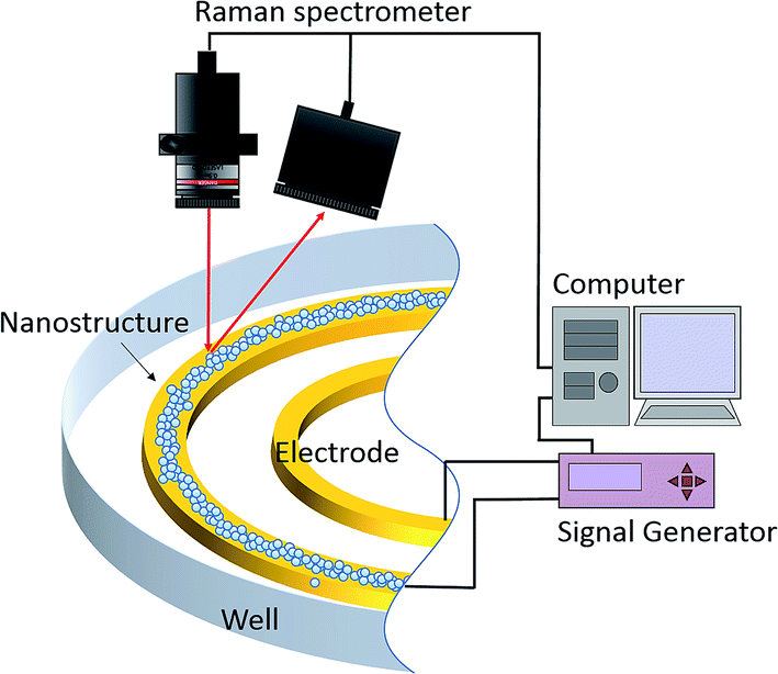
Fig. 1 depicts the in situ SERS platform which possesses dielectrophoresis control due to the higher-order three-dimensional nanostructure gold electrodes. Our basic idea was that dielectrophoresis would be able to control the colloidal particles and aggregation of the three-dimensional nanostructure at the desired position on demand. Fig. 2 shows a schematic of the fabrication process using a mixture of metallic nanoparticles and polystyrene (PS) nanoparticles manipulated by the dielectrophoretic (DEP) force. First, we prepared the pair of electrodes and a well to contain the solution [Fig. 2(a)]. Following addition of the solution, dielectrophoresis was induced by the application of an alternating current (AC) to cause aggregation and construct the higher-order three-dimensional layer stack nanostructure consisting of gold nanoparticles (AuNPs) and PS [Fig. 2(b)]. Fig. 2(c) shows the schematic of structural formation under the competition of aggregation and evaporation of the solution. After evaporation, the higher-order layer stack three dimensional nanostructure, including both AuNPs and PS particles, was formed as shown schematically in Fig. 2(d). Finally, to remove PS after peeling off the poly(dimethylsiloxane) (PDMS) sheet, the assembled higher-order nanostructure was soaked in dichloromethane. We then obtained the novel electrode mounted with the higher-order nanostructure, as shown in Fig. 2(e).
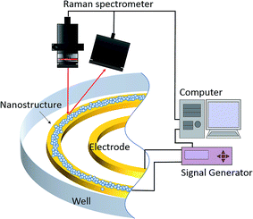 |
| | Fig. 1 Schematic of the novel electrode formation and surface-enhanced Raman spectroscopic system. | |
 |
| | Fig. 2 Schematic of the formation process of the higher-order nanostructure. (a) Cross-sectional cartoon of the electrodes fabricated on the glass substrate by a normal microfabrication process consisting of a combination of UV-lithography and the lift-off method. (b) A mixed solution of polystyrene (PS) beads and Au nanoparticles (AuNPs) is placed in the PDMS well. (c) Schematic of momentary higher-order layer stack nanostructure, including PS and AuNPs, formation through the competitive self-assembly among sedimentation, radial flow, Maragngoni flow, DLVO interactions and DEP force. Schematic images after (d) evaporation of the solution, (e) removing PS and formation of the higher-order nanostructure sustained with only AuNPs. | |
B. Formation mechanism of higher-order nanostructure
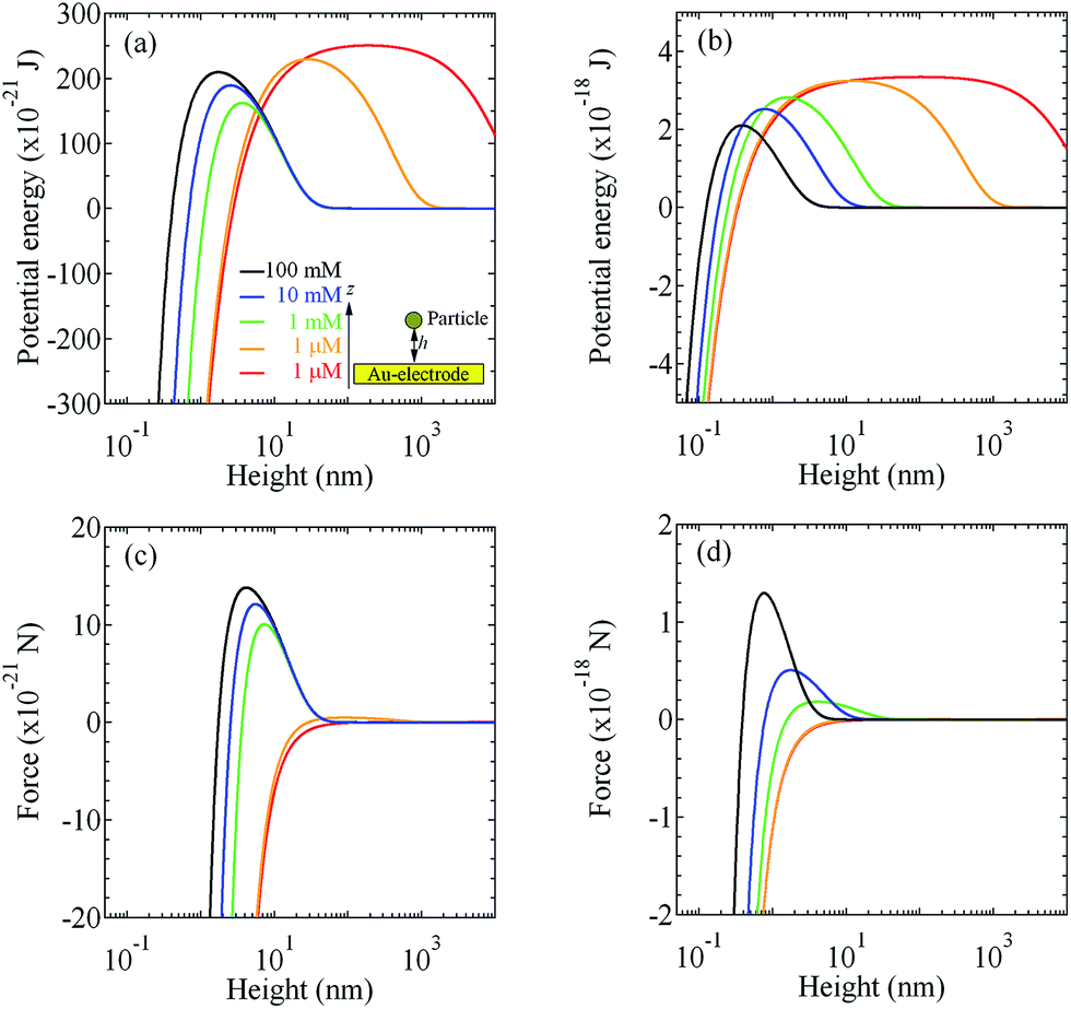
The mechanism of formation of the higher-order layer stack nanostructure is described by the competitive self-assembly14–16 between radial flow, Marangoni recirculating flow, Derjaguin, Landau, Verwey and Overbeek (DLVO) interactions and sedimentation under dielectrophoresis. Here, accordingly to DLVO theory,25–29 the interaction free energy potential between two hetero spheres is described by| |
 | (1) |
where εr and ε0 are the relative permittivity of water and the permittivity of a vacuum, respectively, and ψ1 and ψ2 denote the zeta potentials of spheres 1 and 2, respectively. Here, zeta potentials of AuNPs and PS are assumed to be −46.12 and −41.16 mV, respectively. The radii of AuNPs and PS are 20 and 300 nm, respectively. The Debye screening length Hamaker constant are represented by 1/κ and A132, respectively. Here, the Hamaker constant (A132) represents the interaction between media 1 and 2 through medium 3.
Fig. 3(a)–(c) show the DLVO interaction free potential energies as a function of distance between the particles; PS–PS, PS–AuNP and AuNP–AuNP, respectively. The inset of Fig. 3(a) represents the analytical model of DLVO interaction between hetero particles. All calculations were derived from eqn (1). The forces between the particles was calculated by the differential potential; i.e. F = −∂U/∂x, where U and x denote the potential and coordinate axis, respectively. Fig. 3(d)–(f) display the forces exerted on the particles as a function of the distance.
 |
| | Fig. 3 Potential energies evaluated by the DLVO theory as a function of distance (d) between (a) PS–PS, (b) PS–AuNP and (c) AuNP–AuNP in water under the assumed ion densities of 1 nM, 1 μM, 1 mM, 10 mM and 100 mM. The inset of (a) depicts the schematic model for DLVO interaction between the hetero particles. Forces derived from the gradient of DLVO potentials are represented for (d) PS–PS, (e) PS–AuNP and (f) AuNP–AuNP. | |
Next, we evaluate the higher-order stack layer nanostructure deposition process onto the electrode and substrate using the similar procedure described in our previous study.16 Here, under the assumption that a particle with a spherical radius R stays aloof at a height h between the particle and glass substrate, the interaction free energy between the particle and substrate is given by25–29
| |
 | (2) |
where
ψP and
ψS denote the zeta potentials of the particle and substrate, respectively. Here, zeta potential of glass substrate and Au electrode are adopted to be −66 mV (
ref. 30) and −46.12 mV, respectively. To simplify the calculation, we estimate the calculated potential energies of AuNP–glass substrate and PS–glass substrate are plotted as a function of height
h in
Fig. 4(a) and (b), respectively. The forces between particle and substrate can be calculated by differential potential, that is
F = −∂
U/∂
z.
Fig. 4(c) and (d) show the height dependence of the force between particle and substrate. In the similar way,
Fig. 5(a) and (b) display the potential energies as a function of height
h for the cases of (a) AuNP–Au electrode and (b) PS–Au electrode, respectively. The forces calculated by the respective potential energies (AuNP– and PS–Au electrode) are plotted as shown in
Fig. 5(c) and (d), respectively. As shown in these evaluation results, the DLVO repulsion force prevent the deposition of the particles onto the Au electrode and glass substrate. Here, a particle traveling in a droplet experiences not only DLVO interactions but also other forces. In the vertical direction, hydrodynamic from radial flow and Marangoni flow, sedimentation and DEP forces act to determine the particle height in the fluidic flow profile. Here, we consider the equilibrium, which is the sedimentation dominating the deposition of particles.
 |
| | Fig. 4 Potential energies evaluated by the DLVO theory as a function of height (h) in the cases of (a) AuNP–glass substrate and (b) PS–glass substrate in water under the assumption of ion densities of 1 nM, 1 μM, 1 mM, 10 mM and 100 mM. The inset of (a) depicts the schematic model for DLVO interaction between particle and substrate. Forces derived from the gradient of DLVO potential energies are represented for (c) AuNP–glass substrate and (d) PS–glass substrate. | |
 |
| | Fig. 5 Potential energies as a function of height (h) in the case of (a) AuNP–Au electrode and (b) PS–Au electrode in water under the assumption of ion densities of 1 nM, 1 μM, 1 mM, 10 mM and 100 mM. Evaluated forces are shown in (c) AuNP–Au electrode and (d) PS–Au electrode, respectively. | |
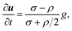
The sedimentation of spherical particle under the constant flow in equilibrium is described by31
| |
 | (3) |
where
u is velocity vector of the particle, that is ∂
u/∂
t represents the acceleration.
σ and
ρ are mass densities of particle and media, respectively.
g is the acceleration due to gravity, that is 9.8 m s
−2. Here, the mass densities of Au, PS and water are 19.3 × 10
3, 1050 and 997 kg m
−3, respectively. Substituting these densities into
eqn (3), the gravitation forces working AuNP and PS are estimated to about 5.86 × 10
−18 and 3.98 × 10
−17 N, respectively. The gravitation forces working AuNP and PS are always larger than the DLVO repulsion forces between particles and substrate. Thus, we show the sedimentation enables us to deposit the particles onto the substrate and Au electrode.
Finally, we present that DEP force can control the deposition of particles in a more aggressive manner. The DEP force exerted on particles with diameter a is given by:32–34
| | |
FDEP = 2πa3εmRe[fCM]∇|E|2,
| (4) |
where
εm and Re[
fCM] are the permittivity of the medium and real part of the Clausius–Mossotti factor, respectively. Here, we estimate each Clausius–Mossotti factor under the low frequency limit as the applied AC electric field was ∼100 kHz, which is almost considered to be a direct current (DC) field. The frequency-dependent complex permittivity can be treated as the conductivity; therefore, we assumed that Re[
fCM] = 1. We used deionized water with a permittivity of
εm = 80
ε0 = 80 × 8.85 × 10
−12 [F m
−1] and σ
m = 5.5 [μS m
−1]. To evaluate the DEP force by varying the particle radius, the medium and AC electric field were fixed.
Fig. 6 shows the particle radius dependence of the DEP force on 50, 100 and 150 μm electrode widths and gaps.
 |
| | Fig. 6 Particle radius dependency of the DEP forces for electrode widths/gaps of 50/50, 100/100 and 150 μm/150 μm. | |
By comparison of the DEP, DLVO interaction and sedimentation forces, we found that the DEP force manipulating the AuNPs and PS particles was larger than the DLVO repulsive forces between particles located away from each other. Thus the DEP forces cause the collection of the particles on the electrode by overcoming the DLVO repulsive force. The closer the particles come to each other, the larger the van der Waals attractive forces become. The AuNPs can then infiltrates the gaps between PS particles, forming aggregates. Therefore, formation of the higher-order layer stack nanostructure is caused by colloidal particle deposition resulting from the competition among sedimentation,16 radial flow, Marangoni flow, DLVO interactions and DEP force, as shown in Fig. 2. In particular, the DEP force can actively trigger the formation of a higher-order laminar nanostructure with AuNPs and PS particles. As shown in Fig. 2, the DEP force enables us to control and coagulate the higher-order nanostructure at our desired position on demand. Here, we demonstrate the novel electrode with a higher-order layer stack Au nanostructure, as shown in Fig. 2(d).
III. Experimental methods
A. Preparation of the Au and polystyrene beads
Au colloids with 20 nm diameters were prepared according to the standard citrate reduction method reported by Lee and Meisel.35 The AuNP dispersion was prepared at 0.48 mM. Polystyrene latex beads (PS) with 600 nm diameters (Invitrogen Inc., 8% w/v) were concentrated by centrifugation and washed to yield a 10% w/v suspension.15,16 The concentration of AuNPs and PS were estimated to be 1.17 × 10¹⁵ and 8.42 × 10¹⁴ particles per L, respectively. AuNPs were concentrated 50-fold by centrifuging at 12![[thin space (1/6-em)]](https://www.rsc.org/images/entities/char_2009.gif) 000 rpm for 15 min twice with one extraction. AuNPs were mixed with PS to prepare various ratios of (i) 700:1, (ii) 1000:1 and (iii) 1300:1 (AuNP:PS).
000 rpm for 15 min twice with one extraction. AuNPs were mixed with PS to prepare various ratios of (i) 700:1, (ii) 1000:1 and (iii) 1300:1 (AuNP:PS).
B. Preparation of the electrode
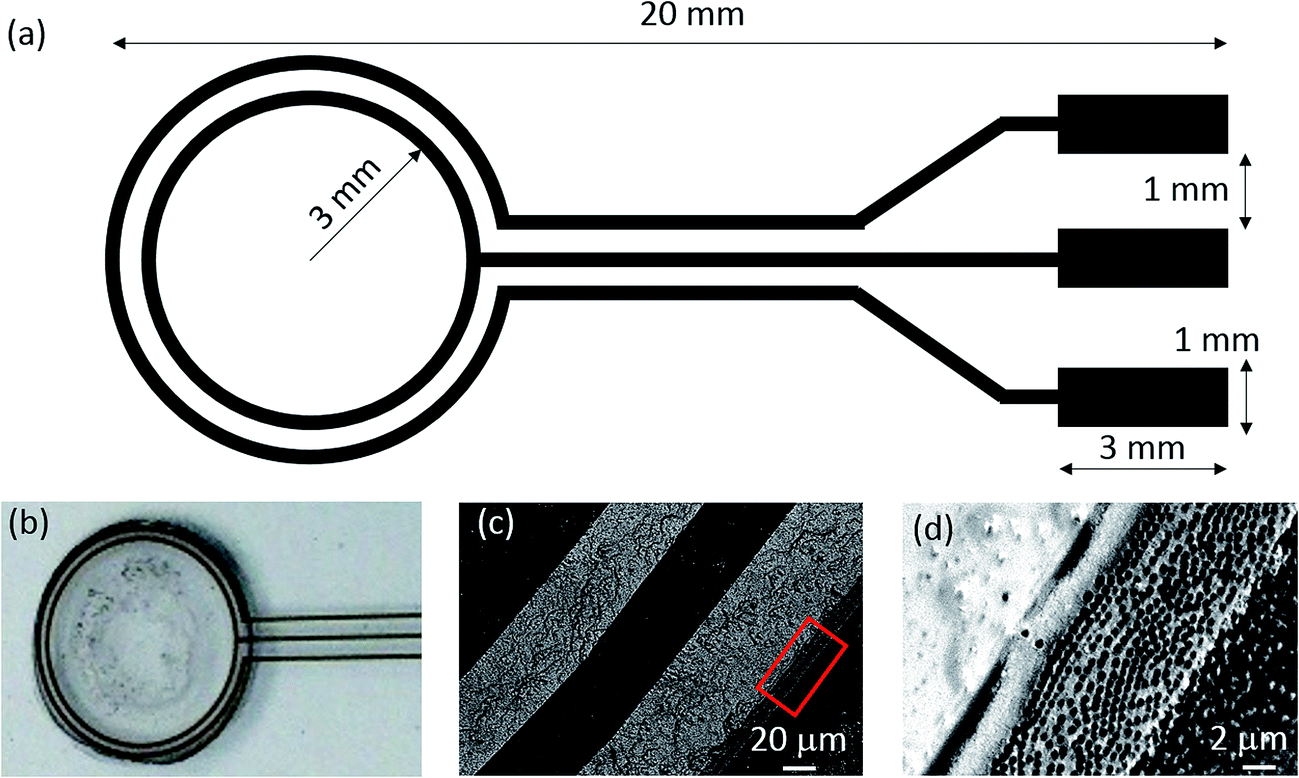
A schematic of the electrodes for dielectrophoresis is shown in Fig. 7, with two circular electrodes arranged in a concentric pattern. These electrodes were fabricated on glass slides (Matsunami Glass Ind., Ltd) by means of standard UV lithography and the lift-off technique. The electrodes prepared from Au (80 nm)/Cr (5 nm) were connected to an arbitrary function generator (Keysight technology, 33510B). We designed the circular electrode with 50, 100 and 150 μm widths and gaps, as this shape enabled us to control the AuNPs and PS particles through dielectrophoresis.
 |
| | Fig. 7 (a) Schematic of the electrode before formation of the higher-order nanostructure in a PDMS well containing a solution of PS and AuNPs. (b) Optical photograph of the electrode after the evaporation of the solution and formation of the higher-order layer stack nanostructure with AuNPs under condition #9. (c) SEM image of the electrodes. (d) Highly magnified SEM image of the outer electrode and higher-order nanostructure. The red square area shown in (c) corresponds to the SEM image displayed in (d). | |
C. Preparation of the system
A silicone sheet with a through hole with 6 mm diameter was placed on an ultraviolet-cleaned glass slide, where the Au electrodes were previously fabricated, and a well was formed. The mixed solution (38 μL) of AuNPs and PS was placed in the well and covered with a cover glass to prevent the droplet from drastically evaporating.
IV. Results and discussion
A. Evaluation of the electrode
Here, we simultaneously applied an AC electric field of 1 to 100 kHz to various concentration of PS and AuNPs in the vicinity of the electrodes. The PS and AuNPs irreversibly formed aggregates and the DEP force did not enable dynamic control of the aggregation and disaggregation. When the maximum number of particles were irreversibly immobilized, the structure was soaked in dichloromethane to remove the PS. All experimental conditions are summarized in Table 1. The higher order nanostructure was successfully obtained under several conditions. Fig. 7(b) shows the optical photograph of the top view of the whole system after forming the nanostructure under condition #9. Scanning electron microscope (SEM) images are displayed in Fig. 7(c) and (d), showing that the formed higher-order layer stack nanostructure was connected to the outer electrode.
Table 1 Summary of experimental conditions
| No. |
Electrode width (μm) |
Frequency (kHz) |
Particle number ratio (Au:PS) |
Higher-order nanostructure |
SERS detection |
| 1 |
50 |
1 |
700:1 |
× |
× |
| 2 |
50 |
1 |
1000:1 |
× |
× |
| 3 |
50 |
1 |
1300:1 |
× |
× |
| 4 |
50 |
10 |
700:1 |
× |
× |
| 5 |
50 |
10 |
1000:1 |
× |
100 μM |
| 6 |
50 |
10 |
1300:1 |
× |
× |
| 7 |
50 |
100 |
700:1 |
× |
100 μM |
| 8 |
50 |
100 |
1000:1 |
× |
× |
| 9 |
50 |
100 |
1300:1 |
○ |
100 nM |
| 10 |
100 |
1 |
700:1 |
× |
× |
| 11 |
100 |
1 |
1000:1 |
× |
× |
| 12 |
100 |
1 |
1300:1 |
○ |
<100 nM |
| 13 |
100 |
10 |
700:1 |
× |
× |
| 14 |
100 |
10 |
1000:1 |
× |
× |
| 15 |
100 |
10 |
1300:1 |
× |
× |
| 16 |
100 |
100 |
700:1 |
× |
× |
| 17 |
100 |
100 |
1000:1 |
× |
× |
| 18 |
100 |
100 |
1300:1 |
× |
100 μM |
| 19 |
150 |
1 |
700:1 |
× |
× |
| 20 |
150 |
1 |
1000:1 |
× |
× |
| 21 |
150 |
1 |
1300:1 |
○ |
100 nM |
| 22 |
150 |
10 |
700:1 |
× |
× |
| 23 |
150 |
10 |
1000:1 |
× |
× |
| 24 |
150 |
10 |
1300:1 |
× |
× |
| 25 |
150 |
100 |
700:1 |
× |
× |
| 26 |
150 |
100 |
1000:1 |
× |
100 μM |
| 27 |
150 |
100 |
1300:1 |
× |
× |
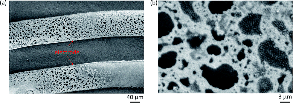
Under condition #12, the higher-order layer stack nanostructure could be mounted on the outer electrode, as shown in Fig. 8. The magnified SEM images [Fig. 8(b) and (c)] demonstrate that the width of the entire nanostructure was approximately 30–40 μm in the radial direction. The higher resolution SEM image [Fig. 8(d)] revealed the formation of a higher-order porous layer stack nanostructure consisting of AuNPs. The two dimensional-like nanostructure was formed under condition #21, as shown in Fig. 9. We found that we were able to fabricate a higher-order nanostructure under only three conditions: #9, #12 and #21. The summary shown in Table 1 indicates that we are able to obtain the electrode with the higher-order layer stack nanostructure only when the ratio of Au:PS was 1300:1, as this provides the quantity of AuNPs required for the conservation of the higher-order nanostructure after the removal of PS. By applying AC fields of 1 and 100 kHz, the particles gathered on the middle and outer side of the outer electrode, respectively. Au electrode with of 50 μm is not considered to be wide enough to form and conserve the higher-order nanostructure. This is why condition #3 could not form the higher-order nanostructure even with the appropriate ratio of Au:PS.
 |
| | Fig. 8 SEM images of the novel electrode with the formation of the higher-order layer stack nanostructure under condition #12. The red square area shown in (a) is magnified in (b). SEM images with high magnification for (c) the electrode and (d) higher-order layer stack porous nanostructure. | |
 |
| | Fig. 9 (a) SEM image of the novel electrode after the formation of the higher-order porous nanostructure under condition #21. (b) SEM image of the higher-order nanostructure fabricated on the electrode. | |
Conversely, the higher-order layer stack nanostructure was formed on the outer side of the outer electrode only under condition #9. This is attributable to the narrow spatial electric field distribution realized on the outer side of the outer electrode. A pearl chain structure appeared under most conditions, as shown in Fig. 10. This is attributable to the migration of AuNPs as a result of dielectrophoresis. Formation of the pearl chain caused by the DEP force induced a deficiency in AuNPs required for the formation of the higher-order nanostructure. In addition, the pearl chain also induced a circulatory shunt between the electrodes and stops the dielectrophoresis, consequently the pearl chain prevented the aggregation of particles. In our experiment, the ratio of AuNPs:PSs suitable to building the higher-order layer stack nanostructure is expected to be occasionally 1300:1. The procedure for the construction of our device is reproducible under the condition which prevent the solution from spilling.
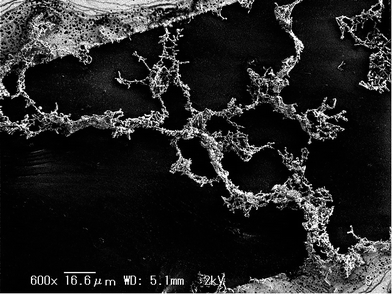 |
| | Fig. 10 SEM image of the pearl chain structure formed under condition #20. | |
Thus, the dielectrophoresis-enabled formation of the higher-order or pearl chain nanostructure was achieved on some level. These nanostructures have the ability to improve surface-enhanced Raman scattering spectroscopy, battery cells, photovoltaic cells, etc.
B. Photoluminescence measurement
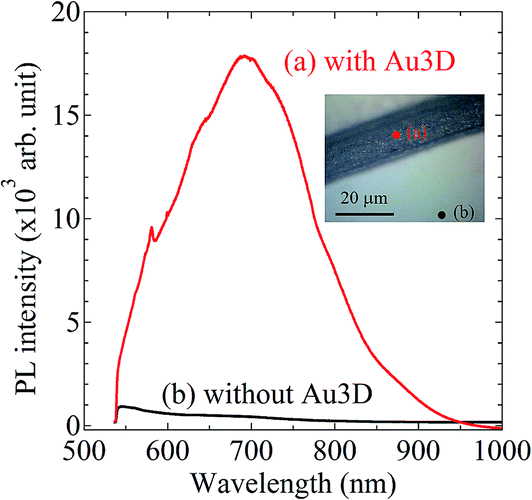
To evaluate the properties of novel Au electrode with higher-order AuNPs layer stack structure, we measured photoluminescence (PL) spectroscopy of the nanostructure and flat Au electrode using the NRS-5100 (JASCO) system. The 532 nm Green laser was used to excite the PL. Fig. 11 shows the PL intensity spectra of Au electrode (a) with and (b) without the higher-order AuNPs layer stack structure. The inset of optical photograph display the measurement positions. As shown in Fig. 11, the large enhancement of the PL spectra from the Au electrode with the higher-order AuNPs layer stack structure is revealed. This result indicates that the higher-order AuNPs layer stack structure can provide electric field enhancement.
 |
| | Fig. 11 Photoluminescence (PL) intensity spectra of Au electrode (a) with and (b) without the higher-order AuNPs layer stack structure. In the inset of optical photograph, (a) the red solid circle and (b) black solid circle correspond to the measurement positions, respectively. | |
C. SERS measurement
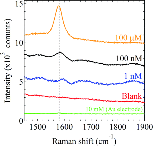
We demonstrated the in situ SERS measurement of 4,4′-bipyridine (4bpy) as a Raman active molecule using the prepared higher-order layer stack gold nanostructure on the electrode formed under condition #12. The silicone sheet with a 6 mm-diameter through hole was placed on the higher order layer stack gold nanostructure on the glass to enable good accurate measurement.15,16,22 An aqueous 4bpy solution (35 μL) with a various concentration was dropped into the well on the higher-order layer stack gold nanostructure. A cover glass was used to prevent the 4bpy solution from evaporating and to maintain its concentration. The higher order layer stack gold nanostructure was placed in the simple Raman spectrometer without microscope (RAM-100S, Lambda Vision Inc.), and a 785 nm wavelength laser (laser power, 50 mW) was used to irradiate the higher order layer stack gold nanostructure for 1 s.
The higher-order layer stack nanostructure enabled us to detect concentrations below 100 nM 4bpy as shown in Fig. 12. Through comparison of all spectra plotted in Fig. 12, the characteristic enhanced Raman spectra of 4bpy (characteristic peak positions at 1000, 1250, and 1582 cm−1) were clearly observed.36 To compare the SERS-activity of flat Au electrode and Au electrode with the higher-order nanostructure, we display the SERS spectrum of 10 mM 4bpy using the flat Au electrode. We afresh confirm the enhancement of SERS-activity induced by the higher-order AuNPs stack layer structure. The peak intensity is dependent on the 4bpy density in the same SERS-active structure, indicating that the correct SERS-activity can be evaluated here. To evaluate the availability of the novel electrode with higher-order layer stack nanostructure, we estimate the SERS enhancement factor (EF). The EF is defined as  , where ISERS and NSERS are the intensity of the SERS signal and the number of molecules contributing to ISERS, respectively.37 INR is the intensity from the normal Raman signal at the same wavenumber at which ISERS is estimated. NNR is the number of molecules contributing to INR. The ratio
  is given by
  . Here, NA is the Avogadro number, C is the concentration of 4bpy (CSERS = 100 nM and CNR = 10 mM), and VSERS and VNR are the total volume of the laser spot. In this study, VSERS is equal to VNR. ISERS and INR of 100 nM and 10 mM at 1582 cm−1 are 483 and 45, respectively. As a result, the EF is estimated to be ∼1.0 × 10⁶ with the fabricated platform using the simple Raman spectrometer without any microscope.
 |
| | Fig. 12 Characteristic enhanced Raman spectra of 4,4′-bipyridine (4bpy) at concentrations of 100 μM, 100 nM, 1 nM, as well as a blank (ultrapure water with the higher-order layer stack gold nanostructure and no analyte) using the Au electrode with the higher-order AuNPs layer stack structure. Raman spectra of 10 mM 4bpy was measured using the flat Au electrode without the higher-order nanostructure. | |
The SERS enhancement factor is simply estimated to be approximately 106, considering that the detection limit of normal usage without the SERS enhancement structure is 10 mM in the simple Raman spectrometer RAM-100S with no microscope. The other electrodes formed under the conditions #9 and #21 enabled us to detect 100 nM 4bpy (data not shown). Thus, we succeeded in obtaining a novel electrode with the SERS-active higher-order layer stack nanostructure consisting of AuNPs. We also found that 100 μM of 4bpy was able to be detected by the pearl chain structure (data not shown). The higher-order nanostructure has an advantage of SERS enhancement compared with the pearl chain structure. This is attributable to that the higher-order layer stack gold nanostructure has more numbers of SERS-active hot site under the field of the Raman spectrometer without microscope (field is about 2 mm × 2 mm) than the pearl chain structure. In addition, the novel electrode with the higher-order layer stack nanostructure provides a clue to enhancing the performance of surface-engineered nanomaterials38 and photothermal films for solar thermoelectric conversion.39
V. Conclusion
We fabricated a novel electrode with sterically bulky three-dimensional Au layer stack nanostructure through the combination of convective phenomena and dielectrophoresis. The essence of the higher-order nanostructure formation process can be explained by the competition between five contributions: radial flow, Marangoni recirculating flow, movement of particles towards the substrate driven by DLVO interactions, sedimentation force and dielectrophoresis. The electrode under conditions which can form the higher-order nanostructure enabled us to detect concentrations as low as below 100 nM 4bpy using a simple Raman spectrometer without a microscope. The SERS enhancement factor was estimated to be approximately 106 times, compared to the case without any higher-order nanostructure. Thus, the novel electrode with the SERS-active higher-order nanostructure consisting of AuNPs will allow for measurement of dynamic signals from biological molecules as well as environmental and chemical reaction processes.
Acknowledgements
We are grateful to Dr M. Ishihara for PL measurement support. This work is partly supported by Strategic Information and Communications R&D Promotion Programme, Kansai Research Foundation for technology promotion, MEXT Grants-in-Aid for Scientific Research in a Priority Area and a JSPS Grants-in-Aid for Scientific Research.
References
- M. G. Albrecht and J. A. Creighton, J. Am. Chem. Soc., 1977, 99, 5215–5217 CrossRef CAS.
- D. L. Jeanmaire and R. P. van Duyne, J. Electroanal. Chem., 1977, 84, 1–20 CrossRef CAS.
- S. M. Nie and S. R. Emory, Science, 1997, 275, 1102–1106 CrossRef CAS PubMed.
- K. Kneipp, Y. Wang, H. Kneipp, L. T. Perelman, I. Itzkan, R. R. Dasari and M. S. Feld, Phys. Rev. Lett., 1997, 78, 1667–1670 CrossRef CAS.
- J. B. Jackson, S. L. Westcott, L. R. Hirsh, J. L. West and N. J. Halas, Appl. Phys. Lett., 2003, 82, 257–259 CrossRef CAS PubMed.
- K.-C. Ho, P.-J. Tsai, Y.-S. Lin and Y.-C. Chen, Anal. Chem., 2004, 76, 7162–7168 CrossRef CAS PubMed.
- S. W. Bishnoi, Y. J. Lin, M. Tibudan, Y. Huang, M. Nakaema, V. Swarup and T. A. Keiderling, Anal. Chem., 2011, 83, 4053–4060 CrossRef CAS PubMed.
- K. E. Peceros, X. Xu, S. R. Bulcock and M. B. Cortie, J. Phys. Chem. B, 2005, 109, 21516–21520 CrossRef CAS PubMed.
- W. Shi, Y. Sahoo, M. T. Swihart and P. N. Prasad, Langmuir, 2005, 21, 1610–1617 CrossRef CAS PubMed.
- T. Kondo, K. Nishio and H. Masuda, Appl. Phys. Express, 2009, 2, 032001 CrossRef.
- S. Akil-Jaradi, S. Jradi, J. Plain, P.-M. Adam, J.-L. Bijeon, P. Royer and R. Bachelot, RSC Adv., 2012, 2, 7837–7842 RSC.
- K. Ikeda, S. Suzuki and K. Uosaki, Nano Lett., 2011, 11, 1716–1722 CrossRef CAS PubMed.
- H. Liu, L. Zhang, X. Lang, Y. Yamaguchi, H. Iwasaki, Y. Inouye, Q. Xue and M. Chen, Sci. Rep., 2011, 1, 112 Search PubMed.
- R. Bhardwaj, X. Fang, P. Somasundaran and D. Attinger, Langmuir, 2010, 26, 7833–7842 CrossRef CAS PubMed.
- R. Takahashi, T. Fukuoka, Y. Utsumi and A. Yamaguchi, Jpn. J. Appl. Phys., 2013, 52, 06GK12 CrossRef.
- R. Hara, T. Fukuoka, R. Takahashi, Y. Utsumi and A. Yamaguchi, RSC Adv., 2014, 5, 1378–1384 RSC.
- D. Mark, S. Haeberle, G. Roth, F. von Stetten and R. Zengerle, Chem. Soc. Rev., 2010, 39, 1153–1182 RSC.
- P. Yager, T. Edwards, E. Fu, K. Helton, K. Nelson, M. R. Tam and B. H. Weigl, Nature, 2006, 442, 412–418 CrossRef CAS PubMed.
- H. Hwang, D. Han, Y.-J. Oh, Y.-K. Cho, K.-H. Jeong and J.-K. Park, Lab Chip, 2011, 11, 2518–2525 RSC.
- A. F. Chrimes, K. Khoshmanesh, P. R. Stoddart, A. A. Kayani, A. Mitchell, H. Daima, V. Bansal and K. Kalantar-Zadeh, Anal. Chem., 2012, 84, 4029–4035 CrossRef CAS PubMed.
- S. Cherukulappurath, S. H. Lee, A. Campos, C. L. Haynes and S.-H. Oh, Chem. Mater., 2014, 26, 2445–2452 CrossRef CAS.
- A. Yamaguchi, R. Takahashi, T. Fukuoka, R. Hara and Y. Utsumi, to be published.
- S. Sriram, M. Bhaskaran, S. Chen, S. Jayawardhana, P. R. Stoddart, J. Z. Liu, N. V. Medhekar, K. K. Zadeh and A. Mitchell, J. Am. Chem. Soc., 2012, 134, 4646–4653 CrossRef CAS PubMed.
- N. T. T. Trang, T. T. Thuy, D. M. Mott, M. Koyano and S. Maenosono, Chem. Phys. Lett., 2013, 574, 94–99 CrossRef CAS PubMed.
- R. Hogg, T. W. Healy and D. W. Fuerstenau, Trans. Faraday Soc., 1966, 62, 1638 RSC.
- J. N. Israelachvili, Intermolecular and Surface Forces, Academic Press, London, 3rd edn, 2011 Search PubMed.
- C. V. Chrysikopoulos and V. I. Syngouna, Colloids Surf., B, 2012, 92, 74 CrossRef CAS PubMed.
- S. Bhattacharjee, M. Elimelech and M. Borkovec, Croat. Chem. Acta, 1998, 71, 883 CAS.
- H.-J. Butt, K. Graf and M. Kappl, Physics and Chemistry of Interfaces, Wiley-VCH GmbH & Co. KGaA, 2003 Search PubMed.
- A. Sze, D. Erickson, L. Ren and D. Li, J. Colloid Interface Sci., 2003, 261, 402 CrossRef CAS.
- L. D. Landau and E. M. Lifshitz, Fluid Mechanics, Pergamon, London, 3rd edn, 1966 Search PubMed.
- T. B. Jones, Electromechanics of Particles, Cambridge University Press, Cambridge, England, 1995 Search PubMed.
- X.-B. Wang, J. Vykoukal, F. F. Becker and P. R. Gascoyne, Biophys. J., 1998, 74, 2689–2701 CrossRef CAS.
- Y. Huang, X. B. Wang, F. F. Becker and P. R. Gascoyne, Biophys. J., 1997, 73, 1118–1129 CrossRef CAS.
- P. C. Lee and D. Meisel, J. Phys. Chem., 1982, 86, 3391 CrossRef CAS.
- S. W. Joo, Vib. Spectrosc., 2004, 34, 269 CrossRef CAS PubMed.
- E. C. le Ru, E. Blackie, M. Meyer and P. G. Etchegoin, J. Phys. Chem. C, 2007, 111, 13794–13803 CAS.
- S. Kawata, in Near-Field Optics and Surface Plasmon Polaritons, Springer, Berlin, 2001 Search PubMed.
- A. Kosuga, Y. Yamamoto, M. Miyai, M. Matsuzawa, Y. Nishimura, S. Hedaka, K. Yamamoto, S. Tanaka, Y. Yamamoto, S. Tokonami and T. Iida, Nanoscale, 2015, 7, 7580–7584 RSC.
|
| This journal is © The Royal Society of Chemistry 2015 |
Click here to see how this site uses Cookies. View our privacy policy here. 


 , where ISERS and NSERS are the intensity of the SERS signal and the number of molecules contributing to ISERS, respectively.37 INR is the intensity from the normal Raman signal at the same wavenumber at which ISERS is estimated. NNR is the number of molecules contributing to INR. The ratio
  is given by
  . Here, NA is the Avogadro number, C is the concentration of 4bpy (CSERS = 100 nM and CNR = 10 mM), and VSERS and VNR are the total volume of the laser spot. In this study, VSERS is equal to VNR. ISERS and INR of 100 nM and 10 mM at 1582 cm−1 are 483 and 45, respectively. As a result, the EF is estimated to be ∼1.0 × 10⁶ with the fabricated platform using the simple Raman spectrometer without any microscope.