
 Open Access Article
 This Open Access Article is licensed under a
 Creative Commons Attribution 3.0 Unported Licence
Solar power generation enhancement of dye-sensitized solar cells using hydrophobic and antireflective polymers with nanoholes
Joo Ho Lim,
Jung Woo Leem and
Jae Su Yu*
Department of Electronics and Radio Engineering, Institute for Wearable Convergence Electronics, Kyung Hee University, 1732 Deogyeong-daero, Giheung-gu, Yongin-si 446-701, South Korea. E-mail: jsyu@khu.ac.kr
First published on 9th July 2015
Abstract
We improve the power conversion efficiency (PCE) of dye-sensitized solar cells (DSSCs) using polydimethylsiloxane (PDMS) patterned with negatively tapered nanoholes (NHs) as a protective antireflection layer of the external glass surface. The NHs PDMS layers are prepared by a soft lithography via silicon molds with conical nanopillars. The NHs PDMS with a NH depth of ∼320 nm decreases the surface reflection of fluorine doped tin oxide (FTO)-coated glass over a wide wavelength range of 350–800 nm at incident angles (θin) of 0–70°, exhibiting a lower solar weighted reflectance (RSW) value of ∼7.1% at θin = 0° and a lower average RSW value of ∼8.5% at θin = 20–70° than those (i.e., RSW ≈ 10.1% at θin = 0° and average RSW ≈ 15.6% at θin = 20–70°) of the FTO glass. In DSSC device applications, it increases the short-circuit current density (JSC) from 15.69 to 16.52 mA cm−2, thus resulting in an enhanced PCE value of 7.56% compared to the reference DSSC (i.e., PCE = 7.15%). For different NH depths, the optical reflectance characteristics of the NHs PDMS/FTO glass are theoretically investigated using a rigorous coupled-wave analysis method, showing similar trends between the calculated and measured results. For solar spectrum angle-dependent photocurrents, it also shows a remarkable device performance at θin = 20–70°. Besides, the NHs PDMS exhibits a hydrophobic surface with a water contact angle of ∼115°.
Introduction
Over the past decades, research into alternative energy sources has been a global issue as a result of enhanced environmental pollution and fossil-fuel consumption. Solar energy, among several other alternative energy sources, has been attracting interest in various application fields because of its abundance, cost-effective production, and environmental friendliness. In particular, comparing the dye-sensitized solar cell (DSSC) with other solar cells, it has some advantages such as low manufacturing cost, lightweight, flexibility, transparency, and so on.1–3 However, the power conversion efficiencies (PCEs) of DSSCs fall below 13%, mainly due to limitations including the light absorption of the dyes and the interface charge separation between dyes and titanium dioxide (TiO2) electrodes.2,3 Hence, possibilities exist for further enhancements in PCEs of DSSCs. In order to boost the light absorption in the dyed TiO2 layer of the devices, among various approaches for improving the PCE, one simple method is the employment of efficient antireflection coatings (ARCs) on the front surface of the substrates. As an alternative of conventional ARCs consisting of single layer or multilayers, recently, many studies have been reported on the nanostructured surfaces (e.g., nanogratings, nanorods, and nanoporous films) on external substrates or covers of solar cells as ARCs.4–7 However, to directly fabricate the nanostructures on substrates, nanopatterning (e.g., electron-beam, nanoimprint, or laser interference lithography) and etching processes including chemical and heat treatments are required, which increase the fabrication cost and complexity. Therefore, it is necessary to develop efficient ARCs of glasses in the effective ways including cost-effective, simple, and high-throughput processes. In this respect, soft lithography, which has been widely utilized to form the various nanostructures onto the surface of polymers, can be one of them.8–11 The fabricated molds and stamps can be also repeatedly used for pattern transfer, and thus would facilitate the mass production (i.e., roll-to-roll or roll-to-plate) in industry applications. In the soft lithography, meanwhile, the dimethylsiloxane (PDMS) is generally used as a protective encapsulation layer against mechanical damage to the underlying devices due to its low free surface energy, flexibility, transparency, and hardness.10–14 Besides, it can increase the optical transmission of transparent substrates including glasses, polymers, etc. because of its lower refractive index of ∼1.4–1.43.14,15 Furthermore, the PDMS layer can be strongly attached on the surface of planar transparent substrates with detachability from it. On the other hand, the hydrophobicity is useful in outdoor applications because it can function the self-cleaning for the pollutants and dusts on the surface of devices.16,17 Thus, it is very meaningful to investigate the optical and wetting behaviors of nanostructured PDMS layers as well as their feasibility on the device performance of DSSCs. In this work, we demonstrated the PCE enhancement of DSSCs via protective AR PDMS layers with nanoholes (NHs) patterns. The NHs on the PDMS layers were negatively transferred from the silicon (Si) molds with tapered nanopillars by the soft lithography. Their optical reflectance characteristics, together with a theoretical prediction using a rigorous coupled-wave analysis (RCWA) method, were also studied at various incident angles of light, including the surface wettability.Experimental and numerical modelling details
Fabrication of NHs PDMS and DSSCs
Fig. 1 shows the schematic diagram for the fabrication procedure of the NHs-patterned PDMS (i.e., NHs PDMS) from the Si mold with tapered nanopillars via the soft lithography. The conical nanopillars on Si molds were prepared by using the thermally dewetted platinum (Pt) nanoparticles as an etch mask pattern and subsequent dry etching process, as reported in our previous work.18 As shown in Fig. 1, to fabricate the NHs on the surface of PDMS layers without any distortion and deformation, we performed two-step coating processes. Firstly, a mixture solution consisting of the trimethylsiloxy terminated vinylmethylsiloxane-dimethylsiloxane (VDT-731; Gelest, Inc.) and methylhydrosiloxane-dimethylsiloxane (HMS-301; Gelest, Inc.) copolymers was spin-coated on the Si molds, and then they were cured at a temperature of 75 °C for 30 min. Afterwards, the Sylgard 184 PDMS (base![[thin space (1/6-em)]](https://www.rsc.org/images/entities/char_2009.gif) :agent = 10:1) solution was poured on the samples with curing at 75 °C for 2 h. Finally, the PDMS layers were carefully separated from the Si molds, creating the NHs PDMS. To study the effect of depth of NHs on the optical reflectance property, the NHs PDMS samples with NH depths of 150 and 320 nm were prepared, named NHs-A at 150 nm and NHs-B at 320 nm, respectively. On the other hand, DSSCs were made by a conventional fabrication process. A TiO2 paste was deposited on fluorine doped tin oxide (FTO)-coated glasses using a doctor-blade method. Then, it was annealed at 500 °C for 2 h in a furnace. The deposition and annealing processes were repeated to fix the thickness of the deposited TiO2 paste by ∼15 μm. For the ruthenium(II) dye (Solaronix, N719), the TiO2 coated FTO glass substrates were immersed in a 3 × 10⁻⁴ M solution with mixing dye for 24 h in dark state. By using the same doctor-blade process, a Pt paste (Dyesol, counter PT-1) as a counter electrode was coated onto the FTO glass substrates. Lastly, an electrolyte (Dyesol, electrolyte HPD) was injected, and thus the DSSCs with an active area of 0.25 cm2 were fabricated.
:agent = 10:1) solution was poured on the samples with curing at 75 °C for 2 h. Finally, the PDMS layers were carefully separated from the Si molds, creating the NHs PDMS. To study the effect of depth of NHs on the optical reflectance property, the NHs PDMS samples with NH depths of 150 and 320 nm were prepared, named NHs-A at 150 nm and NHs-B at 320 nm, respectively. On the other hand, DSSCs were made by a conventional fabrication process. A TiO2 paste was deposited on fluorine doped tin oxide (FTO)-coated glasses using a doctor-blade method. Then, it was annealed at 500 °C for 2 h in a furnace. The deposition and annealing processes were repeated to fix the thickness of the deposited TiO2 paste by ∼15 μm. For the ruthenium(II) dye (Solaronix, N719), the TiO2 coated FTO glass substrates were immersed in a 3 × 10⁻⁴ M solution with mixing dye for 24 h in dark state. By using the same doctor-blade process, a Pt paste (Dyesol, counter PT-1) as a counter electrode was coated onto the FTO glass substrates. Lastly, an electrolyte (Dyesol, electrolyte HPD) was injected, and thus the DSSCs with an active area of 0.25 cm2 were fabricated.
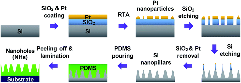 | ||
| Fig. 1 Schematic diagram for the fabrication procedure of the nanoholes-patterned PDMS (i.e., NHs PDMS) from the Si mold with tapered nanopillars via the soft lithography. | ||
Characterization instruments
A scanning electron microscope (SEM; LEO SUPRA 55, Carl Zeiss) was utilized for observing the surface morphologies and pattern profiles of the fabricated samples. The surface wetting behaviors were evaluated by using a contact angle measurement system (Phoenix-300, SEO). A UV-vis-NIR spectrophotometer (Cary 5000, Varian) was used to characterize optical reflectance properties. The current density–voltage (J–V) characteristics of DSSCs were measured by using a photocurrent system consisting of a solar simulator (ABET, SUN 3000) with 1000 W Xe short arc lamp and a source meter (Keithley 2400). Incident photon to current conversion efficiency (IPCE) data were obtained by illuminating monochromatic light on the DSSCs using a 300 W xenon arc lamp as the light source coupled to a monochromator (TLS-300× xenon light source, Newport) with optical power meter (2935-c, Newport).Numerical modelling and simulations
The theoretical analysis on the optical reflectance and the electric field intensity distribution of the NHs PDMS were also studied by the RCWA method using a commercial software (DiffractMOD, Rsoft Design Group). To design the numerical model, the shape of the negatively tapered nanohole structure (i.e., empty space, air) on the surface of the PDMS was represented by a periodic geometry in the Cartesian coordinate system using a scalar-valued function of three variables, f(x, y, z), for simplicity. We assumed that the incident light enters from air to the PDMS layer. The Ey, i.e., amplitude of y-polarized electric field, was calculated for the incident plane wave with a Gaussian beam profile that is normalized at λ = 530 nm. The period of NHs was kept at 280 nm. The thicknesses of constituent layers were set to be 150 μm for the PDMS, 500 μm for the glass, and 650 nm for the FTO film, respectively. The calculated values at each wavelength were averaged to remove rapid fluctuations caused by the interference of light reflected at the top and bottom surfaces of the PDMS/glass/FTO. The refractive index and extinction coefficient of glass and FTO were acquired from index Web site.19 For the PDMS, the refractive index was assumed to be 1.43.Results and discussion
Fig. 2 shows (a) the 40°-tilted oblique-view SEM images of the Si mold with nanopillars and the fabricated PDMS with nanoholes (NHs) and (b) the photographs of a water droplet on the surface of corresponding PDMS samples. Using the soft lithography technique, the negatively tapered nanohole arrays were relatively well transferred onto the surface of the PDMS films from conical nanopillar-structured Si molds (i.e., average height ≈170 nm for the nanopillars-A and ≈380 nm for the nanopillars-B) without any large deformation and distortion, as shown in the SEM images of Fig. 2(a). For the formed NHs on the PDMS films, the average NH depths were estimated to be ∼150 nm (i.e., NHs-A PDMS) and ∼320 nm (i.e., NHs-B PDMS), respectively. The PDMS with a flat surface showed a hydrophobic property with a water contact angle (θCA) of ∼99°.20 The introduction of the roughness on the surface enhances the hydrophobicity, as can be explained by the Cassie–Baxter theory.21 Thus, the larger θCA values were obtained for the NHs PDMS, exhibiting the θCA ≈ 106° for the NHs-A and θCA ≈ 115° for the NHs-B, respectively. This hydrophobic surface might self-clean the dusts and contaminants on the devices in outdoor environments.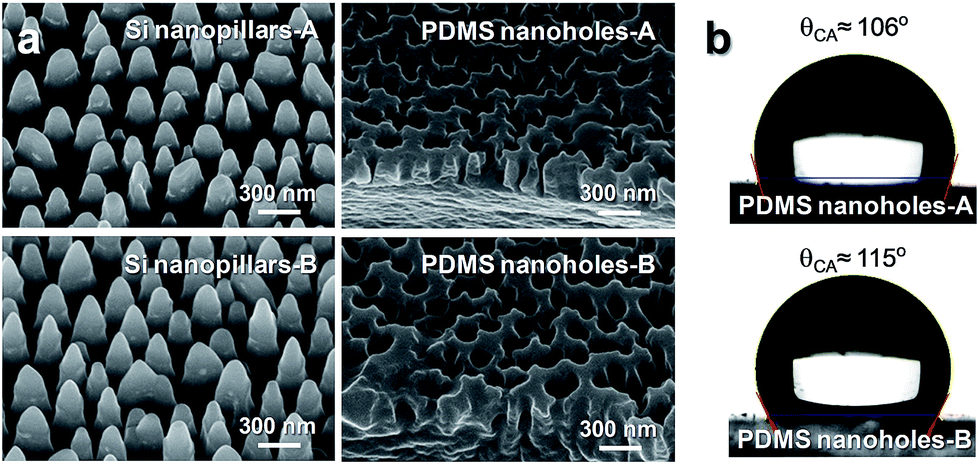 | ||
| Fig. 2 (a) 40°-tilted oblique-view SEM images of the Si mold with nanopillars and the fabricated PDMS with NHs and (b) photographs of a water droplet on the surface of corresponding PDMS samples. | ||
Fig. 3 shows (a) the measured reflectance spectra of the FTO glass, the flat PDMS/FTO glass, the NHs-A PDMS/FTO glass, and the NHs-B PDMS/FTO glass, (b) the contour plot of the variation of the calculated reflectance spectra of NHs PDMS/FTO glass as functions of wavelength and depth of NHs, and (c) the electric field (Ey) intensity distributions for the corresponding structures at λ = 530 nm. As shown in Fig. 3(a), by laminating the flat PDMS on the glass surface of the FTO glass, the surface reflectance of the FTO glass was reduced because of the step gradient refractive index (GRIN) profile in constituent materials of air (n = 1)/PDMS (1.43)/glass (1.52)/FTO (1.98). On the other hand, the NHs PDMS further decreased the reflectance over a wide wavelength range of 350–800 nm. This is attributed to the linear and continuous GRIN profile via negatively tapered NHs (i.e., moth-eye effect).22 For the NHs-B PDMS with a larger NH depth of ∼320 nm, its solar weighted reflectance (RSW) value of ∼7.1%, which is the ratio of the usable photons reflected to the total usable photons,23 at wavelengths of 350–800 nm is lower than those of the other samples (i.e., RSW ≈ 10.1%, 9%, and 7.9% for the FTO glass, the flat PDMS/FTO glass, and the NHs-A PDMS/FTO glass, respectively). In RCWA simulations of Fig. 3(b), the calculated reflectance results of NHs PDMS at different depths of NHs were roughly similar to the experimentally measured spectra in Fig. 3(a). The RSW values of NHs PDMS/FTO glass as a function of depth of NHs are also shown in the inset of Fig. 3(b). The RSW values are abruptly decreased from 9.6% at 0 nm (i.e., flat PDMS/FTO glass) to 7.6% at 200 nm and they are minimally saturated at NH depths of >300 nm, exhibiting RSW values of ∼7.4–7.5%. These results show a similar tendency with the optical properties of transparent materials (e.g., glasses, polymers, etc.) with one-side antireflective nanostructured surface reported in other previous works.24–26 Therefore, it can be considered that the NHs PDMS with the NH depth of ∼320 nm is an optimized sample that has the lowest RSW value of ∼7.1% in the NHs PDMS/FTO glass structure. Additionally, the antireflection characteristics of the NHs PDMS can be observed in the calculated Ey intensity distributions. In Fig. 3(c), for both the glass and flat PDMS, the Ey intensities at λ = 530 nm are high in the air region due to their strong surface reflection. For the NHs PDMS, on the other hand, there exist relatively weaker Ey intensities in the air region due to the suppressed reflectivity caused by the GRIN profile of the NHs on the surface of PDMS.
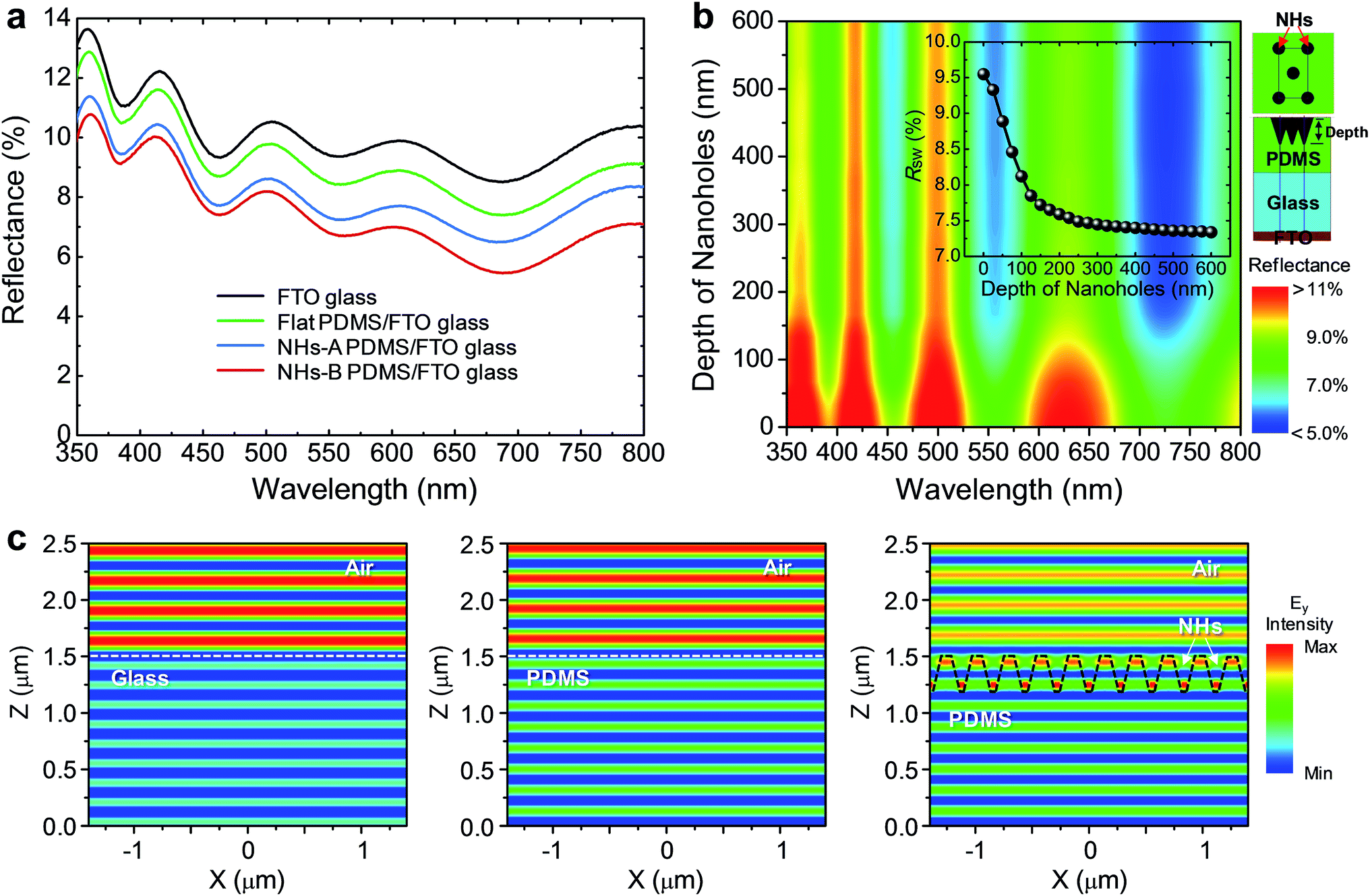 | ||
| Fig. 3 (a) Measured reflectance spectra of the FTO glass, flat PDMS/FTO glass, NHs-A PDMS/FTO glass, and NHs-B PDMS/FTO glass, (b) contour plot of the variation of the calculated reflectance spectra of NHs PDMS/FTO glass as functions of wavelength and depth of NHs, and (c) Ey intensity distributions for the corresponding structures at λ = 530 nm. The RSW values of NHs PDMS/FTO glass as a function of depth of NHs are also shown in the inset of (b). | ||
It is also important to study incident light angle-dependent reflectance characteristics due to the change of the sun position in a day and seasons. Fig. 4 shows (a) the RSW values for the measured reflectance spectra of the FTO glass, the flat PDMS/FTO glass, and the NHs-B PDMS/FTO glass as a function of incident angle (θin) in the wavelength range of 350–800 nm and (b) the contour plots of variations of the calculated angle-dependent reflectance spectra for the corresponding structures. As shown in Fig. 4(a), for all the samples, the RSW values gradually increased with increasing the θin value from 20 to 70°. However, as expected, the NHs-B PDMS with a superior AR ability further decreased the RSW values of FTO glass compared to the flat PDMS at each θin value, exhibiting a lower average RSW value of ∼8.5% at θin = 20–70° (i.e., average RSW values of ∼15.6% and ∼11.9% for the FTO glass and the flat PDMS/FTO glass, respectively). Similarly, in the RCWA calculations of Fig. 4(b), the NHs PDMS/FTO glass shows the less-angle dependent reflectance characteristics compared to the other structures in wide ranges of incident wavelengths and angles.
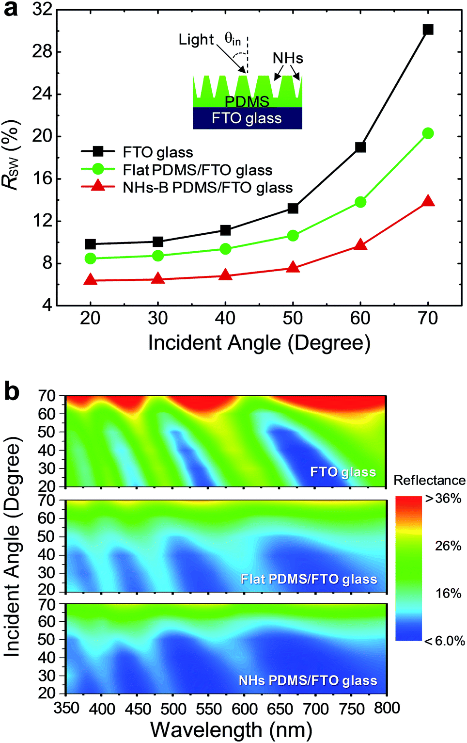 | ||
| Fig. 4 (a) RSW values for the measured reflectance spectra of the FTO glass, the flat PDMS/FTO glass, and the NHs-B PDMS/FTO glass as a function of incident angle (θin) in the wavelength range of 350–800 nm and (b) contour plots of variations of the calculated angle-dependent reflectance spectra for the corresponding structures. | ||
In order to demonstrate the AR effect of the NHs PDMS in DSSCs, the device characteristics of DSSCs employed with NHs PDMS as a protective AR layer were investigated. Fig. 5 shows the (a) J–V curves and (b) IPCE spectra of the reference DSSC without PDMS and the DSSCs with the flat PDMS, the NHs-A PDMS, and the NHs-B PDMS. Photograph of the DSSC incorporated with NHs-B PDMS protective AR layer is also shown in the inset of Fig. 5(b). It can be observed that the PDMS is well laminated on the external glass surface of the DSSC due to van der Waals force between the PDMS and glass. The device characteristics of the corresponding DSSCs are summarized in Table 1. As shown in Fig. 5(a), by laminating the PDMS on the glass surface of DSSCs, the increased short-circuit current density (JSC) values were observed while there was no large variation in both the open-circuit voltage (VOC) and fill factor (FF). The DSSC with the NHs-B PDMS especially exhibited a higher JSC value of 16.52 mA cm−2 than those of the other DSSCs (i.e., JSC = 15.69, 15.92, and 16.22 mA cm−2 for the reference DSSC and the DSSCs with the flat PDMS and the NHs-A PDMS, respectively). This is ascribed to the reduced surface reflection by the linear GRIN profile via NHs on the PDMS in Fig. 3(a), as mentioned above. The increased photocurrent can be also confirmed in the IPCE data of Fig. 5(b). The DSSC with the NHs-B PDMS showed a higher IPCE spectrum compared to the other DSSCs in the wavelength range of 400–800 nm. As a result, the PCE value of the DSSC with the NHs-B PDMS was improved by 7.56% (i.e., PCE = 7.15% for the reference DSSC), indicating the PCE enhancement percentage of ∼5.8%.
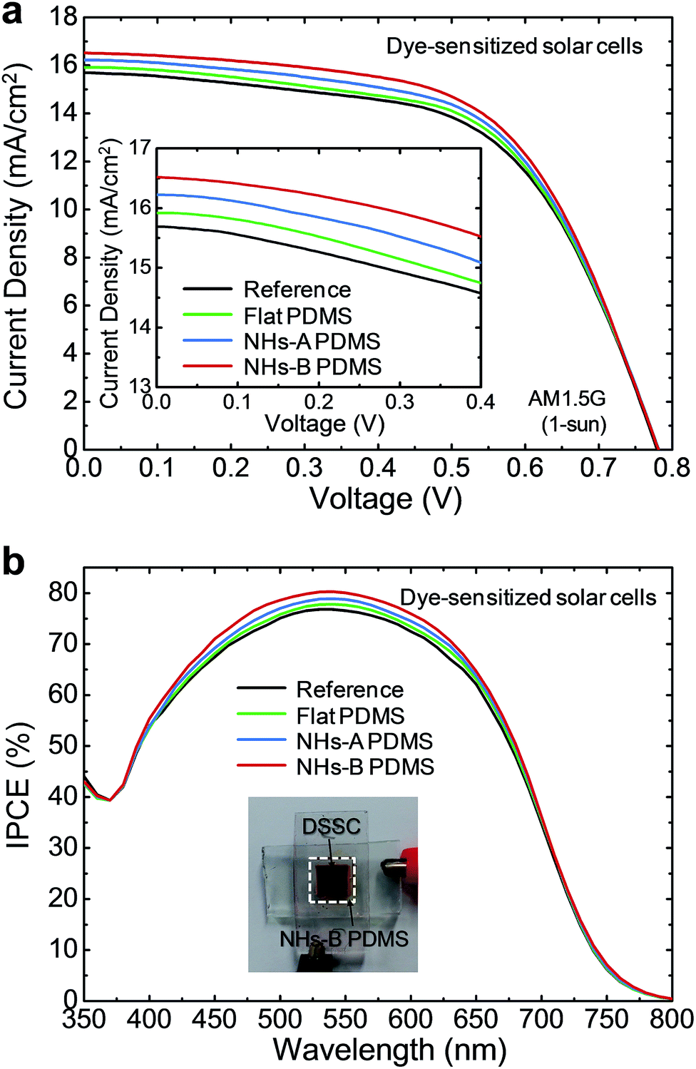 | ||
| Fig. 5 (a) J–V curves and (b) IPCE spectra of the reference DSSC without PDMS and the DSSCs with the flat PDMS, the NHs-A PDMS, and the NHs-B PDMS. Photograph of the DSSC incorporated with NHs-B PDMS protective AR layer is also shown in the inset of (b). | ||
| DSSC | VOC (V) | JSC (mA cm−2) | FF (%) | PCE (%) |
|---|---|---|---|---|
| Reference | 0.780 | 15.69 | 58.44 | 7.15 |
| Flat PDMS | 0.780 | 15.92 | 58.76 | 7.30 |
| NHs-A PDMS | 0.781 | 16.22 | 58.68 | 7.44 |
| NHs-B PDMS | 0.781 | 16.52 | 58.62 | 7.56 |
To study the angle-dependence of solar power generation in DSSCs with the AR NHs PDMS, their JSC values were measured and the enhancement percentage in JSC was estimated for the DSSC with the flat PDMS and the NHs-B PDMS relative to the reference DSSC at θin = 20–70°, as shown in Fig. 6. For all the DSSCs, the JSC values were generally reduced with increasing the θin value. This is attributed to the reduction of the projection area where the incident light enters into the DSSC due to the tilted DSSC from the normally incident light source of the solar simulator as well as the increased surface reflection losses. However, the DSSC with the NHs-B PDMS showed the higher JSC value at each θin value, maintaining a larger average enhancement percentage value of ∼8.8% compared to the reference DSSC at θin = 20–70° (i.e., ∼3.9% for the flat PDMS DSSC/reference DSSC). Thus, the use of the NHs PDMS AR layer with NH depths of >300 nm can lead to the enhancement of the solar energy harvesting in DSSCs for an entire day and the seasons.
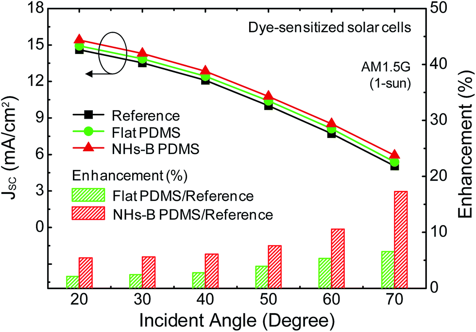 | ||
| Fig. 6 JSC of values the reference DSSC and the DSSCs with the flat PDMS, and the NHs-B PDMS and estimated enhancement percentage in JSC for the DSSCs with the flat PDMS DSSC and the NHs PDMS relative to the reference DSSC at θin = 20–70°. | ||
Conclusions
The inversely tapered NHs were fabricated on the surface of the PDMS by the soft lithography via the Si mold with conical nanopillars and their optical reflectance properties were experimentally and theoretically investigated. For the 320 nm-depth NHs-B PDMS/FTO glass with the hydrophobic surface (i.e., θCA ≈ 115°), it showed the superior AR characteristics at wavelengths of 350–800 nm and θin = 0–70°, exhibiting the lower RSW ≈ 7.1% at θin = 0° and average RSW ≈ 8.5% at θin = 20–70°. By incorporating the NHs-B PDMS into the outer glass of DSSCs as a protective AR layer, the JSC was not only enhanced to 16.52 mA cm−2, but also the IPCE spectrum was increased, thus leading to the improved PCE value of 7.56% (i.e., PCE = 7.15% for the reference DSSC). For incident light angle-dependent photocurrents, it also showed a superior solar power generation ability at θin = 20–70°. These results can provide a deep insight into the nanostructured PDMS for omnidirectional broadband ARCs in various photovoltaic systems that use transparent substrates and covers including glasses and plastics.Acknowledgements
This work was supported by the National Research Foundation of Korea (NRF) grant funded by the Korea government (MSIP) (No. 2014-069441).References
- B. O'Regan and M. Grätzel, Nature, 1991, 353, 737 CrossRef PubMed.
- S. Mathew, A. Tella, P. Gao, R. Humphry-Baker, B. F. E. Curchod, N. Ashari-Astani, I. Tavernelli, U. Rothlisberger, M. K. Nazeeruddin and M. Grätzel, Nat. Chem., 2014, 6, 242 CrossRef CAS PubMed.
- E. Palomares, J. N. Clifford, S. A. Haque, T. Lutz and J. R. Durrant, J. Am. Chem. Soc., 2003, 125, 475 CrossRef CAS PubMed.
- M. L. Brongersma, Y. Cui and S. Fan, Nat. Mater., 2014, 13, 451 CrossRef CAS PubMed.
- Y. C. Wang, B. Y. Lin, P. T. Liu and H. P. D. Shieh, Opt. Express, 2014, 22, A13 CrossRef CAS PubMed.
- Y. Zhang, C. Zhao, P. Wang, L. Ye, J. Luo and B. Jiang, Chem. Commun., 2014, 50, 13813 RSC.
- Y. M. Song, E. S. Choi, G. C. Park, C. Y. Park, S. J. Jang and Y. T. Lee, Appl. Phys. Lett., 2010, 97, 093110 CrossRef PubMed.
- J. Zhang, S. She, X. X. Dong and L. S. Chen, Opt. Express, 2014, 22, 1842 CrossRef CAS PubMed.
- J. W. Leem, M. Choi and J. S. Yu, ACS Appl. Mater. Interfaces, 2015, 7, 2349 CAS.
- Y. M. Song, Y. Xie, V. Malyarchuk, J. Xiao, I. Jung, K. J. Choi, Z. Liu, H. Park, C. Lu, R. H. Kim, R. Li, K. B. Crozier, Y. Huang and J. A. Rogers, Nature, 2013, 497, 95 CrossRef CAS PubMed.
- M. Choi, J. W. Leem and J. S. Yu, RSC Adv., 2015, 5, 25616 RSC.
- T. Bhuvana, B. Kim, X. Yang, H. Shin and E. Kim, Angew. Chem., Int. Ed., 2013, 52, 1180 CrossRef CAS PubMed.
- K. Bao, X. N. Kang, B. Zhang, T. Dai, C. Xiong, H. Ji, G. Y. Zhang and Y. Chen, IEEE Photonics Technol. Lett., 2007, 19, 1840 CrossRef CAS.
- F. Galeotti, F. Trespidi, G. Timò and M. Pasini, ACS Appl. Mater. Interfaces, 2014, 6, 5827 CAS.
- S. M. Azmayesh-Fard, L. Lam, A. Melnyk and R. G. DeCorby, Opt. Express, 2013, 21, 11889 CrossRef CAS PubMed.
- J. Zhu, C. M. Hsu, Z. Yu, S. Fan and Y. Cui, Nano Lett., 2010, 10, 1979 CrossRef CAS PubMed.
- Y. B. Park, H. Im, M. Im and Y. K. Choi, J. Mater. Chem., 2011, 21, 633 RSC.
- J. W. Leem, K. S. Chung and J. S. Yu, Curr. Appl. Phys, 2012, 12, 291 CrossRef PubMed.
- SOPRA, N&K Database (2015), retrieved 2015, <http://refractiveindex.info> Search PubMed.
- J. H. Lim, Y. H. Ko, J. W. Leem and J. S. Yu, Opt. Express, 2015, 23, A169 CrossRef PubMed.
- A. B. D. Cassie and S. Baxter, Trans. Faraday Soc., 1944, 40, 546 RSC.
- D. G. Stavenga, S. Foletti, G. Palasantzas and K. Arikawa, Proc. R. Soc. A, 2006, 273, 661 CAS.
- J. W. Leem, Y. M. Song and J. S. Yu, Nanoscale, 2013, 5, 10455 RSC.
- Y. M. Song, H. J. Choi, J. S. Yu and Y. T. Lee, Opt. Express, 2010, 18, 13063 CrossRef CAS PubMed.
- K. Choi, S. H. Park, Y. M. Song, Y. T. Lee, C. K. Hwangbo, H. Yang and H. S. Lee, Adv. Mater., 2010, 22, 3713 CrossRef CAS PubMed.
- J. W. Leem, Y. Yeh and J. S. Yu, Opt. Express, 2012, 20, 4056 CrossRef CAS PubMed.
| This journal is © The Royal Society of Chemistry 2015 |