
 Open Access Article
 This Open Access Article is licensed under a
 Creative Commons Attribution 3.0 Unported Licence
Low-temperature nanoredox two-step sintering of gelatin nanoskin-stabilized submicrometer-sized copper fine particles for preparing highly conductive layers†
Tetsu Yonezawa*,
Hiroki Tsukamoto and
Masaki Matsubara
Division of Materials Science and Engineering, Faculty of Engineering, Hokkaido University, Kita 13 Nishi 8, Kita-ku, Sapporo, Hokkaido 060-8628, Japan. E-mail: tetsu@eng.hokudai.ac.jp
First published on 7th July 2015
Abstract
A conductive paste was prepared with submicrometer-sized copper fine particles that were coated by a gelatin nanoskin. The average particle size was ca. 130 nm. After drying, an oxidation–reduction two-step sintering process was proposed for these submicrometer-sized copper fine particles to obtain low-resistivity layers at a very low temperature. The optimized conditions gave a low resistivity of 8.2 × 10⁻⁶ Ω cm, even when the particles were covered by a common polymer. Our results suggest that the formation of the small copper oxide prominences on the surface of the copper fine particles could be reduced at low temperatures, forming connected submicrometer-sized metallic copper particles.
Introduction
The unique properties of metal nanoparticles and fine particles provide possible new product developments.1–4 At present, nanotechnology is a technology that cuts across different boundaries, including use in construction and composite materials,5 as catalysts,6–9 antibacterial coatings,10,11 biosensors,12 plasmonic photo devices,13 and electrical devices,14–19 in addition to some consumer products. The steady increase in nanoparticle and fine particle use is accompanied with larger production, requiring development of the handling and processing of such materials.Moreover, the recent intensive progress in printed electronics has been based on the development of materials, including nanomaterials.15–18 In particular, conductive inks and pastes that consist of metal nanoparticles and fine particles are key materials in printed electronics, as they provide a cost-saving wet process application.16–23 This modern printing process technology is expected to open the door for new manufacturing techniques that increase productivity while reducing energy and resource consumption compared to conventional methods. For flexible, lightweight, and inexpensive electronic devices, such as smart labels that include radio-frequency identification (RFID), organic light-emitting diodes (OLEDs), flexible displays, printed electronics will be frequently used to make cost-effective and eco-friendly products.24 Noble metals, in particular the silver nanoparticle inks, are highly stable and often used for producing conductive films.16 However, the high material cost still hinders their use in large-scale printed electronic applications. Silver migration is also an important issue, as it can degrade device performance. Conducting polymers are other possible alternatives, but in many cases, their conductivity is insufficient for industrial use. In contrast, copper nanoparticles and fine particles are attractive from a cost and anti-migration viewpoint. Recently, the synthesis of copper nanoparticles and fine particles has attracted considerable interest.25–42 However, due to their poor resistance to oxidation, only a few papers have been reported thus far on their practical application as electro-conductive materials. From the printed electronic material viewpoint, the presence of copper oxides on the particle surface has negative consequences, as it increases the required sintering temperature and reduces the electro-conductivity. To overcome the copper nanoparticle and fine particle oxidation issue, numerous attempts have been made, including new sintering technologies,26–33 antioxidation,34 encapsulation of the copper surface with polymers,35–38 organic molecules,39 metal oxides,40 and metal shells.41
Yabuki et al. applied a two-step sintering method to a copper layer formed from a copper ink containing 20 nm copper nanoparticles covered by a thin carbon layer.27 A 1 h annealing step in air followed by a 1 h reductive sintering step under 5% hydrogen (H2) in argon (Ar) gas mixture at 300 °C provided a copper layer with a low resistivity of 1.4 × 10⁻⁵ Ω cm. We previously applied a similar two-step sintering method to a layer obtained from a copper ink containing 46 nm copper nanoparticles covered by gelatin.43 After annealing the copper layer at 200 °C under 10 ppm oxygen (O2) in nitrogen (N2) gas flow for 1 h, it was then reduced at 250 °C by 3% H2 in N2 gas flow for 1 h. A low resistivity of 5.1 × 10⁻⁶ Ω cm was obtained. Recently, we have also reported two-step sintering process at 250 °C in air and in 3% H2 in N2 gas with ecologically prepared amine-stabilized copper fine particles and discussing the formation of copper oxide nano-objects on the particle surface and the effect of sintering temperatures on resistivity.44 However, to our best knowledge, a detailed discussion on the mechanisms of the low-temperature two-step sintering process of polymer-stabilized copper fine particles that produces highly conductive copper layers at relatively low temperature as 200 °C has not been discussed so far.
In our previous study, we proposed the use of gelatin as a stabilizer and antioxidation reagent for copper nanoparticles and fine particles prepared by a chemical reduction of copper(II) oxide (CuO)35 and a copper salt.36 CuO is a solid copper source containing oxygen as the only counter anion. From the contamination point of view, CuO is the ideal metal source candidate for copper fine particles used in conductive inks and pastes. Furthermore, this process can be performed at a copper concentration of 1 mol dm−3 (i.e., 64 g of Cu per 1 dm3 of water),35 which is significantly higher than the usual chemical reduction process. Once these gelatin-stabilized copper fine particles were obtained, conductive pastes were prepared and used as the inner electrode material in a multi-layer ceramic capacitor (MLCC).14 We also formed a conductive copper layer by a two-step sintering process at 200 °C and 250 °C using the Cu nanoparticles coated with a gelatin layer,43 however, this previous study could not reveal the mechanism of this low-temperature sintering. Moreover, this copper nanoparticle ink did not contain any sintering binders, which are usually used in industrial processes.
In this paper, we describe the low-temperature sintering process of copper films made from the gelatin-stabilized copper fine particle ink using ethyl cellulose as an organic binder, via the two-step annealing method. The detailed mechanism of this two-step annealing was examined through X-ray diffraction (XRD) and electron microscopy analyses. The oxidative annealing produces smaller prominences of Cu2O, which play a key role in the sintering process. The resultant conductive copper films show a low resistivity of 8.2 × 10⁻⁶ Ω cm. Compared to our previous studies, we performed a sintering process that simulated an industrial process due to using a copper ink that included organic binders.
Experimental
Materials
The CuO microparticles used as the metal source were supplied from Nisshin Chemco (Kyoto, Japan) and had an average diameter of approximately 4 μm. Cu2O was purchased from Kanto (Japan). Hydrazine monohydrate, used as a reducing reagent, and aqueous ammonia (28%) for pH adjustment were purchased from either Wako or Junsei Chemical (Japan). Gelatin (cow origin, MW = ca. 20![[thin space (1/6-em)]](https://www.rsc.org/images/entities/char_2009.gif) 000) and a polyamine type dispersed agent were supplied from Nitta Gelatin NA Inc. (Osaka, Japan). EC vehicle, containing 10 wt% of ethyl cellulose, was purchased from Nisshin-Kasei Co., Ltd., (Japan). Water was purified by an Organo/ELGA Purelabo ultra (>18 MΩ).
000) and a polyamine type dispersed agent were supplied from Nitta Gelatin NA Inc. (Osaka, Japan). EC vehicle, containing 10 wt% of ethyl cellulose, was purchased from Nisshin-Kasei Co., Ltd., (Japan). Water was purified by an Organo/ELGA Purelabo ultra (>18 MΩ).
Preparation of the copper fine particles
The detailed preparation procedure is described in Fig. 1. The copper fine particles were prepared following a method described previously.35 32 g of gelatin was dissolved into hot water (950 cm3, 60 °C), and then the CuO microparticles (80 g) were introduced into this solution. Then, aqueous ammonia (28%) was added to adjust the dispersion pH to ca. 11. The reduction of CuO (80 g, 1 mole) to metallic copper using the hydrazine monohydrate (120 cm3) was carried out at 80 °C in air with stirring for 2 h. The fine particles were then collected by decantation after introducing a saturated aqueous citric acid solution to reduce the dispersion pH to ca. 8.5 and washed with water twice and ethanol twice again, followed by drying the collected copper fine particles at 60 °C under N2 atmosphere. | ||
| Fig. 1 Schematic illustration of the detailed preparation procedure for obtaining gelatin nanoskin-stabilized copper fine particles. | ||
Preparation of the copper fine particle paste and conductive copper film
In order to prepare a paste of the copper fine particles, the collected copper particle powder was first ground by an automatic mortar for 30 min, pulverized by a blender, and mixed with 5 wt% of a dispersing agent. Then the mixture was dispersed into 50 wt% of commercially available paste vehicle using a mixer and an emulsifier. The obtained copper paste was deposited on a glass and an aluminum oxide (Al2O3) substrates (supplied by Furuuchi Chem., Japan) by the doctor blade method for a film with 40 μm thickness and 20 mm width. After drying in N2 at 60 °C for 1 h, the Al2O3 substrate was cut into 20 mm × 20 mm pieces and annealed at 200 °C in air for 4 h, and subsequently reduced in 3% H2 in N2 gas. The reductive annealing times were varied from 1 to 4 h to determine the reduced state of copper. The gas flow rates were adjusted to 2 dm3 min−1 for both air and 3% H2 in N2 gas during annealing.Characterization
Scanning electron microscopic (SEM) images of the particles were performed using a JEOL JSM-6701F field emission type SEM with an acceleration voltage of 15 kV. In this study, secondary electron observation images (SEI) and back scattered electron images for observation of the composition of samples (BEI-COMPO) were taken. SEI gives topological information of sample surfaces. BEI-COMPO was used to understand the composition of the surface of the samples. Heavier elements show brighter contrasts. XRD patterns were obtained with a Rigaku Mini Flex II (Cu Kα). Transmission electron microscopic (TEM) images were obtained with a Hitachi H-9500 with an acceleration voltage of 300 kV. The TEM samples included the annealed copper layer that was detached from the Al2O3 substrate by scratching, then dispersed in ethanol and applied to carbon-coated copper grids. The thermal properties of the copper fine particles and copper oxide particles were measured by thermogravimetric (TG) analysis with a Shimadzu DTG-60H. The TG measurements of the copper paste and the sintered copper film were carried out under air. After the measurement up to 600 °C, all metallic copper was oxidized to CuO and organic molecules were supposed to be totally decomposed and eliminated. The sheet resistances of the copper films were obtained using a four-point probe method (Loresta-GP, MCP-T610, Mitsubishi Chemical Analytech Co., Japan). In order to obtain reproducible data, six points were measured with a four point probe per a copper layer, as shown in Fig. S1,† and the average values are displayed here.Results and discussion
Preparation and characterization of the gelatin-nanoskin stabilized copper fine particles
Copper fine particles with uniform sizes could be obtained readily and reproducibly by our process.35 After the reaction and pH control by citrate addition, the obtained copper fine particles were collected by decantation, washed by water and ethanol to remove excess gelatin molecules at room temperature, and dried under N2 flow at moderated temperature (60 °C). The powders showed no obvious particle oxidation, and no color change of the dried particles was observed for several weeks, as reported elsewhere.35 The XRD pattern of the as-prepared copper fine particles is shown in Fig. S2.† As shown in Fig. 2a, the particles were uniform and nearly spherical, with an average particle size and a size distribution of 120 ± 35 nm. The surface of the particles was covered by the gelatin layer,36 forming a smooth surface with no small dots observed. Gelatin molecules have amino groups and mercaptan groups in their side chains, and they are coordinated to the particle surface. If surface of metallic copper particles is oxidized, small dots should be observed because of the difference of density between metallic Cu and copper oxide (CuO or Cu2O). The copper fine particles were formed by the gradually supply of Cu2+ ion from the surface of CuO microparticles in the presence of excess amount of hydrazine. Thus, supply rate of Cu2+ ion limited the reaction, resulting in the formation of submicron sized uniform copper fine particles. | ||
| Fig. 2 SEM images of the copper particles prepared and used in this study. (a) The as-synthesized copper particles. (b) A cross-sectional image of copper particles printed on an Al2O3 substrate. (c) A SEI (secondary electron) image of the copper particles on the printed layer surface. (d) A BEI-COMPO (back scattered electron for composition) image, detecting reflected electrons, of the copper particles on the printed layer surface. | ||
Preparation of the copper fine particle paste and printing
After purification of the collected copper fine particles, they were then re-dispersed to form a viscous electro-conductive paste. The liquid component of the paste vehicle evaporated at around 120 °C and the ethyl cellulose decomposed at temperatures over 210 °C (Fig. S3†). The obtained copper paste was stable and could be printed with a uniform thickness onto an Al2O3 substrate using doctor blading. After printing, the copper layer was dried at 60 °C under N2 flow to avoid oxidation. Fig. 2b–d show the surface and cross-section SEM images of the as-printed copper particle layers. Copper particle layers with a flat surface and a relatively uniform thickness of ca. 4.0 μm, ranging from 3.0 to 5.0 μm, were obtained (Fig. 2b). Fig. 2c and d are the surface SEM images at the same position taken with a secondary electron detection (SEI) mode and back scattered detection for composite observation (BEI-COMPO) mode. In a BEI-COMPO image, the image contrast is affected not only by the topological structure but also by the atomic number of the materials. Therefore, the bright contrast in BEI-COMPO images shows copper metallic cores of the particles (Fig. 2d). By comparing these two images, one can clearly understand that the copper fine particles are completely covered by polymer layers, including the gelatin, dispersant, and ethyl cellulose. Copper metallic cores did not contact directly to others due to these polymer layers. According to these polymer layers, these as-printed copper particle layers were not electro-conductive.Copper layers after annealing in air and hydrogen–nitrogen mixed gas
The copper thin layers on substrates were first annealed at 200 °C under airflow to effectively remove the organic components, and then subsequently annealed under 3% H2 in N2 gas. After the oxidative annealing in air at 200 °C for 4 h, the surface of the copper layer was also observed by SEM (Fig. 3). The images in Fig. 3 are quite different from those shown in Fig. 2. In Fig. 3a (the secondary electron image), a rough surface of large spherical particles and small prominences (which appear to be spherical particles) was observed. The large particles were connected via the small 10 nm size prominences. The BEI-COMPO image (Fig. 3b) indicated that the smaller prominences, with their bright contrast, consisted of copper. However, a comparison of these two images revealed that the organic components were not completely removed by this oxidative annealing. The areas marked by arrows in Fig. 3b, for example, are considered as organic components based on a comparison of the two SEM images. | ||
| Fig. 3 SEM images of the copper particle layer surface after oxidative annealing. (a) A SEI (secondary electron) image and (b) a BEI-COMPO (back scattered electron for composition) image, with the red arrows marking areas of organic material. | ||
X-ray diffractograms of the copper layers before and after annealing are displayed in Fig. 4. As discussed in our previous paper,35 the copper fine particles were not oxidized in their powder form. After they were re-dispersed in a copper particle paste and flatly printed on an Al2O3 substrate, a small, broad peak corresponding to Cu2O (111) (2θ = 36.4°) was observed. After annealing in air, this peak became larger but remained broad, suggesting that a small quantity of Cu2O was generated on the copper particle surface, corresponding to the SEM images in Fig. 3. After annealing in air, the copper layer contained 29 wt% Cu2O and 71 wt% metallic copper, calculated using the reference intensity ratio (RIR) method.
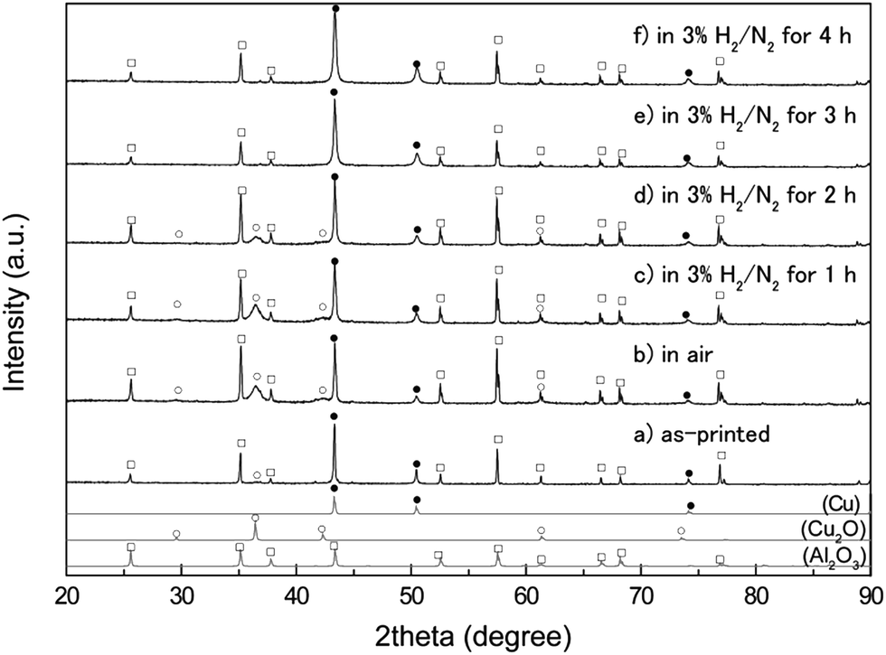 | ||
| Fig. 4 XRD patterns of the copper layer on an Al2O3 substrate before and after annealing. (a) The as-printed copper layer, (b) the layer after oxidative annealing, and the layer after reductive annealing for (c) 1 h, (d) 2 h, (e) 3 h, and (f) 4 h. The metallic copper, the Cu2O, and the Al2O3 peaks are marked as closed circles (●), open circles (○), and open squares (□), respectively. | ||
The annealed substrates were then again annealed at 200 °C, but the gas was changed to 3% H2 in N2 gas mixture (reductive annealing). The reductive annealing time was varied from 1 to 4 h. As observed in Fig. 4, the XRD peak intensity corresponding to Cu2O decreases with the reductive annealing time. First, the surface of the film containing Cu2O was partially reduced to form copper under reductive annealing for 1 h (Fig. 4c). Compared with the XRD patterns of oxidative annealed films (Fig. 4b), the very small change in intensity of Cu2O peaks can be observed. A resistivity of the oxidative annealed film was 25 Ω cm, which indicates that the oxidative annealed film was not conductive. The resistivity dramatically changed, however, after 1 h of reductive annealing, to 7.4 × 10⁻⁵ Ω cm. Thus, reductive annealing makes the film electro-conductive. This is probably due to the connecting of surface metallic copper which was generated by the reductive annealing. The surface metallic copper formed necking during reductive annealing and increased the conductivity. But this reduction of Cu2O to Cu cannot be observed in the XRD patterns. After additional 1 h of reductive annealing, more than half of Cu2O was reduced to metallic copper (Fig. 4c and d). The resistivity and the average thickness of the film reduced for 2 h were 2.7 × 10⁻⁵ Ω cm and 3.3 μm (Fig. 6c).
The XRD pattern (Fig. 4e) indicates that Cu2O was completely reduced by annealing for more than 3 h at 200 °C, and a low resistivity of 8.2 × 10⁻⁶ Ω cm was achieved. A very small peak observed at 36.88° in Fig. 4e and f (which cannot be found in the Al2O3 pattern of JCPDS card) can be attributed to the Al2O3 substrate used for sintering (Fig. S4†). This resistivity is almost 5 times of that of the bulk copper (1.7 × 10⁶ Ω cm). Thus, the complete reduction of the inside Cu2O is necessity to achieve the low resistivity. Additional 1 h of reductive annealing (total 4 h) did not decrease the resistivity. Resistivities of the reductive annealed films are summarized in Fig. 5. On the other hand, TG measurement of commercially available Cu2O particles was performed in this mixed reductive gas, and the change in mass versus time is shown in Fig. S3.† The Cu2O had a slight change in mass under 3% H2 in N2 during the reduction at 200 °C for 2 h. Thus, ∼2 μm size Cu2O particles (SEM image shown in Fig. S5†) are not usually reduced by these conditions. However, the XRD patterns of the reduced films revealed that the Cu2O was completely reduced at 200 °C for 3 h of annealing time, forming metallic copper. We will discuss below about the mechanism of Cu2O reduction at a lower temperature.
 | ||
| Fig. 5 Resistivity of the reductive annealed copper films with various annealing time. The resistivity of bulk copper (1.7 × 10⁻⁶ Ω cm) is marked as the red dotted line. | ||
The surface and cross-sectional SEM images after this reductive annealing step for 2 h are shown in Fig. 6. Necking45–49 of the copper particles and connections between particles were clearly observed in SEI image of Fig. 6a. The cross-sectional image (Fig. 6c) clearly indicates that the necking and connections were observed not only at the surface region but also near the substrate. Fig. 6b shows the BEI-COMPO image of the copper layer surface. Compared with Fig. 6a, the areas marked by arrows can be considered the organic components.
 | ||
| Fig. 6 SEM images of copper layers printed on an Al2O3 substrate after the reductive annealing for 2 h. (a) A SEI image of the surface. (b) A BEI-COMPO image of the surface with the red arrows marking areas of organic material. (c) A cross-sectional image of the reduced layer. | ||
High-resolution TEM (HRTEM) observation of copper layers after annealing
For further investigation, we carried out a HRTEM observation of the annealed copper thin film scratched from the Al2O3 substrate (Fig. 7). As shown in Fig. 7c, after heating under airflow at 200 °C, small prominences less than ca. 10 nm in size were evident on the surface of the copper particles. These nano-sized Cu2O were clearly observed in our previous report about the in situ heating TEM observation of Cu oxidation.45 The lattice fringe distances (2.5 Å and 3.1 Å) observed in the HRTEM images shown in Fig. 7e and f allowed us to identify these prominences as Cu2O (111) and (110), respectively. These images strongly support a formation mechanism of the oxidative annealing in air at 200 °C producing small prominences of Cu2O (<10 nm) covering the metallic copper particles. | ||
| Fig. 7 (a–f) TEM images of the copper particles after oxidative annealing in air, (b) larger magnification image of the boxed area shown in (a). (c and d) A HRTEM image with a higher magnification of the boxed area in (b). Small particles ca. 10 nm in size can be observed in (c). (e and f) Lattice fringes of the Cu2O (111) and (110), respectively, can be observed. (g) TEM image of the copper particles after the reductive annealing of 2 h. (h) Enlarged TEM image of the part of (g) with a higher magnification. (i) TEM image of the copper particles after the reductive annealing for 4 h. (j) Selected area electron diffraction (SAED) image of the square shown in (i). Diffraction spots are assigned as metallic copper. | ||
Fig. 7g–j show the TEM images of the copper film annealed under the reductive gas for 2 h (g and h) 4 h (i and j). Fig. 7g and h are displaying the necked particles. During the oxidation of the copper particle surface, the diffusion of oxygen ions and copper ions into the surface of copper particle first occurs, resulting in formation of copper oxides.45 Then, the particle swelled due to the difference in density between the copper (8.94 g cm−3) and copper oxide (Cu2O: 6.04 g cm−3). This swelling allowed the particle surface to partially contact nearby particles, resulting in an aggregate formation suitable for sintering. The prominences that were below 10 nm in size could lead to the necking between particles. Thus, sintering of the particles progressed due to the melting point depression resulting from the Cu2O nanoscale prominences (generated in the heating under air) reducing to form copper again. The selected area electron diffraction (SAED) image of the copper layer after the reductive sintering is shown in Fig. 7j. The diffraction spots indicate that the obtained layer was consisted of metallic copper.
Low-temperature sintering mechanism of the submicrometer-sized copper fine particles that produces electro-conductive layers
Fig. 8 shows the TG result of copper particles paste. The measurement was carried out under air flow (200 cm3 min−1) with the heating rate of 0.5 °C min−1. The liquid component of paste (48 wt%) was firstly evaporated below 120 °C. After measurement, the copper was completely oxidized and changed into CuO. However, the value of 56.3 wt% includes the weight loss of decomposed polymer components such as the gelatin, the dispersing agent, and the ethyl cellulose. The initial copper ratio of the paste can be calculated as 0.563/1.25 = 0.450 with use of the ratio of MW(CuO)/MW(Cu) = 79.545/63.546 = 1.25. Thus, the amount of the polymer is calculated as 52.0 − 45.0 = 7 wt%. It contains not only gelatin but also vehicles, ethyl cellulose, required to obtain a stable paste. The detailed oxidation behavior of copper particles can be observed between 100 and 250 °C. The gelatin-stabilized metallic copper particles can be oxidized at higher temperatures than ca. 120 °C under air. Cu2O forms initially on the copper particle surface then. The mass in the TG thermogram increased above 120 °C, before decreasing again above 165 °C. As shown in the TG thermogram of the paste vehicle used in this study (Fig. S3†), the decomposition of ethyl cellulose in the commercial paste vehicle starts at 160 °C and lasts at temperatures higher than 200 °C. Therefore, annealing at 200 °C is insufficient to eliminate all the organic components from the copper paste. Fig. 9 shows TG result of the sintered copper film with 3 h of reductive annealing. TG measurement was also carried out under air flow (200 cm3 min−1) and the heating rate of 5 °C min−1. The oxidation of Cu started at ca. 120 °C. Above 160 °C, the decomposition of polymers occurred at the same time. After measurement, the copper was completely oxidized and changed into CuO. However, the value of 117 wt% also includes the weight loss of decomposed organic components. The initial copper ratio of sintered sample can be calculated as 1.17/1.25 = 0.94. From this result, we can estimate that the copper layer after sintering contained 6 wt% of organic components. The copper paste used to prepare copper layer contained 7 wt% of polymers, including gelatin, dispersant and ethyl cellulose. | ||
| Fig. 8 Thermogravimetric (TG) curve of the gelatin-stabilized copper paste. The heating rate was 0.5 °C min−1. (Inset) An enlarged view of the TG curve between 100 and 250 °C, showing an increase in the mass beginning at 120 °C, then decreasing again above 165 °C. | ||
 | ||
| Fig. 9 TG chart of the sintered copper film with 3 h of reductive annealing. The sample was scratched from a glass substrate. TG measurement was carried out under air flow (200 mL min−1) and the heating rate of 5 °C min−1. After measurement, the copper changed into the copper oxide (CuO), so that the initial copper ratio was MW(Cu)/MW(CuO) = 117/125 = 0.94. The organic component ratio was estimated as 6 wt%. | ||
With our low temperature sintering, all organic components were not removed from the copper layer by sintering. However, formation of prominences of Cu2O by oxidative sintering followed by the reductive sintering at a low temperature generated metallic copper neckings to form a conductive copper layer. These results indicate that the polymers used for the copper paste can play also an important role of antioxidizing stabilizers of the sintered metallic copper layer under ambient conditions.
From the results and discussion above, the sintering mechanism of our two-step annealing process can be illustrated, as shown in Fig. 10. First, the copper fine particles were surrounded by an organic layer. Then, the diffusion of oxygen ions and copper ions into the surface of copper particle occurred45 and small prominences of Cu2O, ca. 10 nm in size, which were attached to the copper fine particles, were produced via the oxidative annealing. As the grass transition temperature (Tg) of gelatin is about 80 °C, gas molecules can be penetrate and diffused easily in the polymer layers and can react with copper and copper oxide surfaces. Finally, these Cu2O prominences were reduced again to form the particle necking. Kim et al. reported the time-dependent reduction of Cu2O powder under 5% H2 in Ar gas at 200 °C.50 They also showed that a higher reduction temperature gives a shorter sintering period and the reduction of Cu2O powder at 200 °C completed in 450 min. Our reduction completed much faster than their result. In our system, the Cu2O particle size is less than 10 nm as shown in Fig. 7b and in the previous in situ TEM observation.46 Compared with micro- and nano-particles, the Cu2O particle size may strongly affect their reduction. If the particle size of Cu2O is larger than 1 μm, the reduction temperature increases above 400 °C.51 At 200 °C, only 3 wt% of Cu2O micro-particles (∼2 μm) were reduced under 3% H2 in N2 gas for 20 h of annealing (Fig. S5 and S6†). This result indicates that only 10 nm of depth from the surface were reduced. Thus, the Cu2O particles size of 10 nm is enough small to enable an easy reduction. Our sintering mechanism can be explained that the nano-sized Cu2O prominences enable and accelerate the reduction at low-temperature. Using this two-step annealing, we successfully achieved the low resistivity due to formation of particle necking without removing all polymer layers.
 | ||
| Fig. 10 Schematic of the necking and connection formation between the copper fine particles by our two-step annealing process. | ||
Conclusions
In conclusion, we performed an oxidative–reductive two-step annealing at 200 °C of 130 nm sized copper fine particles to obtain a highly conductive copper layer, even though the organic components included in the copper fine particle paste did not fully decompose at this temperature. After annealing the copper layer in air, Cu2O prominences with the size of less than 10 nm were generated on the copper particle surface, connecting together through the organic layers. These Cu2O nanoprominences could then be reduced to generate metallic copper nanoparticles, connecting the copper cores. Necking of the copper fine particles were observed along with their connections after the reductive annealing. The obtained film resistivity was as low as 8.2 × 10⁻⁶ Ω cm. Our results clearly indicate that using small copper nanoparticles is not the only solution for a low-temperature sintering process.Acknowledgements
This work is partially supported by Grant-in-Aid for Scientific Research A (24241041 to TY) from JSPS, Japan, NEDO, Japan and The Shinsei Foundation, Japan. We also thank Nitta Gelatin Inc. for gelatin supply.Notes and references
- Nanoparticles, ed. G. Schmid, Wiley-VCH, Weinheim, 2011 Search PubMed.
- N. Li, P. Zhao and D. Astruc, Angew. Chem., Int. Ed., 2014, 53, 1756–1789 CrossRef CAS PubMed.
- N. Yan, C. Xiao and Y. Kou, Coord. Chem. Rev., 2010, 254, 1179–1218 CrossRef CAS PubMed.
- N. Toshima and T. Yonezawa, New J. Chem., 1998, 22, 1179–1201 RSC.
- S. Kango, S. Kalia, A. Celli, J. Njuguna, Y. Habibi and R. Kumar, Prog. Polym. Sci., 2013, 38, 1232–1261 CrossRef CAS PubMed.
- F. Viñes, J. R. B. Gomes and F. Illas, Chem. Soc. Rev., 2014, 43, 4922–4939 RSC.
- N. Toshima, T. Yonezawa and K. Kushihashi, J. Chem. Soc., Faraday Trans., 1993, 89, 2537–2543 RSC.
- Z. Zhang, H. Che, Y. Wang, X. She, J. Sun, P. Gunawan, Z. Zhong and F. Su, ACS Appl. Mater. Interfaces, 2012, 4, 1295–1302 CAS.
- S. Liu, Y. Wang, Y. Zhu, G. Wang, Z. Zhang, H. Che, L. Jia and F. Su, RSC Adv., 2014, 4, 7826–7833 RSC.
- S. Chernousova and M. Epple, Angew. Chem., Int. Ed., 2013, 52, 1636–1653 CrossRef CAS PubMed.
- K. Kawai, T. Narushima, K. Kaneko, H. Kawakami, M. Matsumoto, A. Hyono, H. Nishihara and T. Yonezawa, Appl. Surf. Sci., 2012, 262, 76–80 CrossRef CAS PubMed.
- K. Saha, S. S. Agasti, C. Kim, X. Li and V. M. Rotello, Chem. Rev., 2012, 112, 2739–2779 CrossRef CAS PubMed.
- P. K. Jain, X. Huang, I. H. El-Sayed and M. A. El-Sayed, Plasmonics, 2007, 2, 107–118 CrossRef CAS.
- T. Yonezawa, S. Takeoka, H. Kishi, K. Ida and M. Tomonari, Nanotechnology, 2008, 19, 145706 CrossRef PubMed.
- Y.-C. Liao and Z.-K. Kao, ACS Appl. Mater. Interfaces, 2012, 4, 5109–5113 CAS.
- W. Shen, X. Zhang, Q. Huang, Q. Xu and W. Song, Nanoscale, 2014, 6, 1622–1628 RSC.
- Y. Zhang, P. Zhu, G. Li, T. Zhao, X. Fu, R. Sun, F. Zhou and C.-p. Wong, ACS Appl. Mater. Interfaces, 2014, 6, 560–567 CAS.
- S. Krishnan, A. S. M. A. Haseeb and M. R. Johan, IEEE Trans. Compon., Packag., Manuf. Technol., 2012, 2, 587–592 CrossRef CAS.
- T. Wang, X. Chen, G.-Q. Lu and G.-Y. Lei, J. Electron. Mater., 2007, 36, 1333–1340 CrossRef CAS.
- H. Alarifi, A. Hu, M. Yavuz and Y. N. Zhou, J. Electron. Mater., 2011, 40, 1394–1402 CrossRef CAS.
- X.-F. Tang, Z.-G. Yang and W.-J. Wang, Colloids Surf., A, 2010, 360, 99–104 CrossRef CAS PubMed.
- C.-L. Lee, K.-C. Chang and C.-M. Syu, Colloids Surf., A, 2011, 381, 85–91 CrossRef CAS PubMed.
- D. Mott, J. Galkowski, L. Wang, J. Luo and C.-J. Zhong, Langmuir, 2007, 23, 5740–5745 CrossRef CAS PubMed.
- A. C. Arias, J. D. MacKenzie, I. MacCulloch, J. Rivnay and A. Salleo, Chem. Rev., 2010, 110, 3–24 CrossRef CAS PubMed.
- J. Perelaer, P. J. Smith, D. Mager, D. Soltman, S. K. Volkman, V. Subramanian, J. G. Korvink and U. S. Schubert, J. Mater. Chem., 2010, 20, 8446–8453 RSC.
- D. Deng, Y. Jin, Y. Cheng, T. Qi and F. Xiao, ACS Appl. Mater. Interfaces, 2013, 5, 3839–3846 CAS.
- A. Yabuki and N. Arriffin, Thin Solid Films, 2010, 518, 7033–7037 CrossRef CAS PubMed.
- A. Yabuki, N. Arriffin and M. Yanase, Thin Solid Films, 2011, 519, 6530–6533 CrossRef CAS PubMed.
- G. Qin, A. Watanabe, H. Tsukamoto and T. Yonezawa, Jpn. J. Appl. Phys., 2014, 53, 096501 CrossRef.
- B. Kang, S. Han, J. Kim, S. Ko and M. Yang, J. Phys. Chem. C, 2011, 115, 23664–23670 CAS.
- B.-Y. Wang, T.-H. Yoo, Y.-W. Song, D.-S. Lim and Y.-J. Oh, ACS Appl. Mater. Interfaces, 2013, 5, 4113–4119 CAS.
- T. Ishizaki and R. Watanabe, J. Mater. Chem., 2012, 22, 25198–25206 RSC.
- W.-S. Han, J.-M. Hong, H.-S. Kim and Y.-W. Song, Nanotechnology, 2011, 22, 395705 CrossRef PubMed.
- S. Magdassi, M. Grouchko and A. Kamyshny, Materials, 2010, 3, 4626–4638 CrossRef CAS PubMed.
- M. Tomonari, K. Ida, H. Yamashita and T. Yonezawa, J. Nanosci. Nanotechnol., 2008, 8, 2468–2471 CrossRef CAS PubMed.
- T. Yonezawa, N. Nishida and A. Hyono, Chem. Lett., 2010, 39, 548–549 CrossRef CAS.
- Y. Lee, J.-r. Choi, K. J. Lee, N. E. Stott and D. Kim, Nanotechnology, 2008, 19, 415604 CrossRef PubMed.
- Y. Jianfeng, Z. Guisheng, H. Anming and Y. N. Zhou, J. Mater. Chem., 2011, 21, 15981–15986 RSC.
- J. Xiong, Y. Wang, Q. Xue and X. Wu, Green Chem., 2011, 13, 900–904 RSC.
- Y. Kobayashi and T. Sakuraba, Colloids Surf., A, 2008, 317, 756–759 CrossRef CAS PubMed.
- M. Grouchko, A. Kamyshny and S. Magdassi, J. Mater. Chem., 2009, 19, 3057–3062 RSC.
- J. S. Kang, H. S. Kim, J. Ryu, J. H. T. Hahn, S. Jang and J. W. Joung, J. Mater. Sci.: Mater. Electron., 2010, 21, 1213–1220 CrossRef CAS.
- K. Ida, M. Tomonari, Y. Sugiyama, Y. Chujyo, T. Tokunaga, T. Yonezawa, K. Kuroda and K. Sasaki, Thin Solid Films, 2012, 520, 2789–2793 CrossRef CAS PubMed.
- Y. Yong, T. Yonezawa, H. Tsukamoto and M. Matsubara, J. Mater. Chem. C, 2015, 3, 5890–5895 RSC.
- T. Yonezawa, Y. Uchida and Y. Abe, J. Nanosci. Nanotechnol., 2014, 14, 5402–5407 CrossRef CAS PubMed.
- T. Narushima, H. Tsukamoto and T. Yonezawa, AIP Adv., 2012, 2, 042113 CrossRef PubMed.
- W.-r. Lee, Y. S. Lim, S. Kim, J. Jung, Y.-K. Han, S. Yoon, L. Piao and S.-H. Kim, J. Mater. Chem., 2011, 21, 6928–6933 RSC.
- D. Demirskyi, D. Agrawal and A. Ragulya, Scr. Mater., 2010, 62, 552–555 CrossRef CAS PubMed.
- Y. Kobayashi, T. Shirochi, Y. Yasuda and T. Morita, Int. J. Adhes. Adhes., 2012, 33, 50–55 CrossRef CAS PubMed.
- J. Y. Kim, J. A. Rodriguez, J. C. Hanson, A. I. Frenkel and P. L. Lee, J. Am. Chem. Soc., 2003, 125, 10684–10692 CrossRef CAS PubMed.
- Y. Yasuda, E. Ide and T. Morita, Open Surf. Sci. J., 2011, 3, 123–130 CrossRef CAS.
Footnote |
| † Electronic supplementary information (ESI) available: Schematic illustration of the six measuring points of Al2O3 substrate for resistivity measurements (Fig. S1); XRD pattern of as-synthesized copper fine particles on a glass substrate (Fig. S2); TG charts of the paste vehicle including ethyl cellulose under air and N2 flow (Fig. S3); TG and temperature charts of the commercially available Cu2O particles under 3% H2 in N2 gas mixture (Fig. S4); SEM image of commercially available Cu2O particles (Fig. S5). See DOI: 10.1039/c5ra06599b |
| This journal is © The Royal Society of Chemistry 2015 |