
The inelastic electron tunneling spectroscopy of curved finite-sized graphene nanoribbon based molecular devices
Zongling Ding*ab,
Zhaoqi Suna,
Guang Lia,
Fanming Menga,
Mingzai Wua,
Yongqing Maa and
Xiaoshuang Chenc
aSchool of Physics and Material Science, Anhui University, Jiu Long Road 111, Hefei, 230601, China. E-mail: zlding@ahu.edu.cn; Fax: +86-551-6386-1257; Tel: +86-551-6386-1257
bCo-operative Innovation Research Center for Weak Signal-Detecting Materials and Devices Integration, Anhui University, Jiulong Road NO.111, Hefei, 230601, China
cNational Lab. of Infrared Physics, Shanghai Institute for Technical Physics, Chinese Academy of Sciences, Yu Tian Road 500, Shanghai, 230083, China. E-mail: xschen@mail.sitp.ac.cn; Fax: +86-21-6583-0734; Tel: +86-21-3505-2062
First published on 10th June 2015
Abstract
The inelastic electron scattering properties of the molecular devices of curved finite-sized graphene nanoribbon (GNR) slices have been studied by combining the density functional theory and Green's function method. Based on the extended molecular models, the inelastic electron tunneling spectroscopy, inelastic quantum conductance and inelastic current have been calculated systematically. The temperature dependences of the inelastic electron tunneling spectroscopy (IETS) and inelastic current have been discussed. Results show that the contributions of the inelastic conductance increase obviously and become comparable to the elastic conductance for curved GNR slices based junctions. The electron inelastic scattering of the curved GNR-based junctions are orders of magnitude stronger than that of the plane ones. The obvious dependences of the elastic and inelastic current of the finite-sized GNR slices make it have probable applications in molecular microprobes.
Introduction
Due to their remarkable structural, electrical and chemical properties, graphene based low-dimensional carbon materials have been widely studied both on theoretically and experimentally grounds.1–6 In addition to the unique electronic properties, graphene sheets also have very good flexibility and mechanical properties. Graphene and related materials are ideally suited for applications in flexible and plastic electronics.7–10 Meanwhile, with the development of experimental method, people can prepare, characterize and control extremely small scale systems even a single molecule. For practical applications, nano-scale molecular devices based on extremely small graphene nanoribbon (GNR) sheets become possible. The electronic properties of graphene nano-scale sheets are strongly dependent on their geometry.11 The electronic properties of curved graphene nano-scale sheets are considerably different from those of their plane counterparts. It is worth mentioning that the flexible touch screen panels12 of graphene have been indeed realized. In practical applications, the curvature dependence of elastic and inelastic current for the finite-sized GNR based junctions makes it have probable applications in molecular microprobes.Inelastic electron tunneling spectroscopy (IETS) was developed in the 1960s to study vibrational spectra of organic molecules buried inside metal-oxide–metal junctions and has since become a powerful spectroscopic tool for molecular identification and chemical bonding investigations.13–20 There are many significant theoretical works on the topic of IETS have been reported.21–25 The inelastic tunneling process is induced by the coupling between the atom motion and electrons, thus the inelastic transport properties of molecular devices are very sensitive to the configuration. In addition, IET process is closely related to the molecular energy level, molecular motion, the charge transfer and chemical reaction process. It is known that the inelastic component can lead to a second tunneling path, which gives an additional current contribution to the tunneling current if the transmission is far below unity. While in case of a close to unity transmission the inelastic current can reduce the current (have a negative sign) by producing a “dip” in the IET spectrum. Generally, the inelastic contribution to the current is small compared to the elastic tunneling current and is more clearly seen as a peak in the second derivative of the current to the bias voltage. Investigations with IETS have had significant technological implications because they give structural information about the molecular junction and provide a direct access to the dynamics of energy relaxation and thermal dissipation during the electron tunneling. Therefore, the studied of the effect of curvature on the elastic and inelastic electronic and transport properties of graphene nanoscale sheets is necessary.
Theory and calculation methods
The calculations of geometric optimization and electronic properties are performed by the density functional theory in B3LYP level.26,27 Mixed basis set have been used, that is, using the 6-31G basis set for carbon and hydrogen atoms and LanL2DZ basis set for Au atoms. The elastic and inelastic transport properties are carried out using the quantum chemistry for molecular electronics (QCME) code.28–30 The approach for both elastic and inelastic scattering is based on scattering theory and Green's functional theory. The finite-sized GNR based molecular device was decomposed into three parts, the source, the drain and the extended molecule. When energetic constraints are satisfied, the electron crossing the junction may exchange a definite amount of energy with the molecular nuclear motion, resulting in an inelastic component in the transmission current.31 To describe the electron-vibronic coupling effect, molecular theory based on vibrational normal modes has been introduced to the scattering model. In the adiabatic Born-Oppenheimer approximation, the purely electronic Hamiltonian of the molecular systems can be considered parametrically as dependent on the vibrational normal modes Q. Therefore, the total electron tunneling current (I) in the junctions include the contributions of elastic (Iel) and inelastic (Iinel) electron scattering from the source to drain electrode.| I = Iel + Iinel | (1) |
Typically, only a fraction of tunneling electrons has involved in the inelastic tunneling process. The small conductance change induced by the electron-vibronic coupling is commonly measured by the second harmonics of a phase-sensitive detector for the second derivative of the tunneling current d2I/dV2 or the part normalized by the differential conductance (d2I/dV2)/(dI/dV).
By using a Taylor expansion, the nuclear motion depended wave function can be expanded along each vibrational normal mode. Since most IETS are measured at the electronic off-resonant region (that is, conducting levels are far from the Fermi energy), the adiabatic harmonic approximation can be applied. We can then use the first derivative to represent the vibrational motion part in the wave functions. In this case, the total quantum conductance is described as
 | (2) |
Results and discussions
Models
In this article, a series of Au(111)-4 × 4-extended-molecule-Au(111) junctions with different distances between the source and drain electrodes (dSD from 1.37 nm to 1.77 nm) have been considered as the model systems. A concise figure of the molecular devices is given in Fig. 1. The 4 × 4 prototype graphene nanoribbon slice with 8 carbon atoms on the zigzag (ZZ) edges and 8 carbon atoms on the armchair (AC) edges as the basic molecular core. All of the dangling edge carbon atoms on the both sides of ZZ and AC edges have been passivated by hydrogen atoms. The extended molecules are composed of GNRs sandwiched between triangle gold clusters. The introductions of a large number of metal atoms in the system often bring magnitude growth of the quantum chemistry calculations. Furthermore, the main and most important IETS information comes from the vibrations of the molecule atoms and the vibration of electrode metal atoms almost have no effect on the IETS spectra of the device. Therefore, we choose triangle gold clusters composed of three gold atoms to describe source and drain electrodes of the extended molecules. In the geometry optimization process, the coordinate of the Au atoms have been fixed and the atoms of molecular core are fully optimized. We have studied systematically on the effect of fixed electrodes on the geometric and transport properties of GNR slices based molecular devices in one of our previous work.33 The results shown that with different dSD, the central atomic plane exhibited different degrees of curvature. Here, we are mainly interested in the effect of curvature on the inelastic tunneling spectroscopy of finite-sized GNR slices based junctions. It is worth mentioning that for the junction models Au atoms are connected with the molecular core through hydrogen atoms. This actually has a large contact resistance. Therefore, if one choose other atoms with small contact resistance (such as sulphur atom), the conductance should increase significantly. | ||
| Fig. 1 Structures of the 4 × 4 GNR based molecular junctions. | ||
The elastic and inelastic quantum conductances of curved 4 × 4 GNRs-based junctions
It is known that in the nanomolecular devices, electrons scatter from the ground state in the source reservoir to an excitation level, and transport through the conducting channel to the ground state in the drain reservoir. The molecular orbitals of the extended molecule serve as the conducting channels. The inclusion of nuclear motion introduces vibrational excited states in the electronic ground state potential. These vibrational excited states are the ones that contribute to the inelastic terms in the case of off-resonant excitation. Meanwhile, the electron can also tunnel through the molecular orbitals, resulting in the elastic term in the total current. Therefore, the total quantum conductance in the junctions can be divided into two parts, the elastic and inelastic electron scattering from source to drain electrodes. The calculated elastic and inelastic quantum conductance (here, we plot as G/G0 with G0 = 2e2/h being the conductance quantum, bias voltage = 2 V, at room temperature) curves of a series of 4 × 4 GNR-based molecular devices with different dSD and curvature radius have been given in Fig. 2. The black solid lines are for the elastic and red dashed lines are for the inelastic conductance.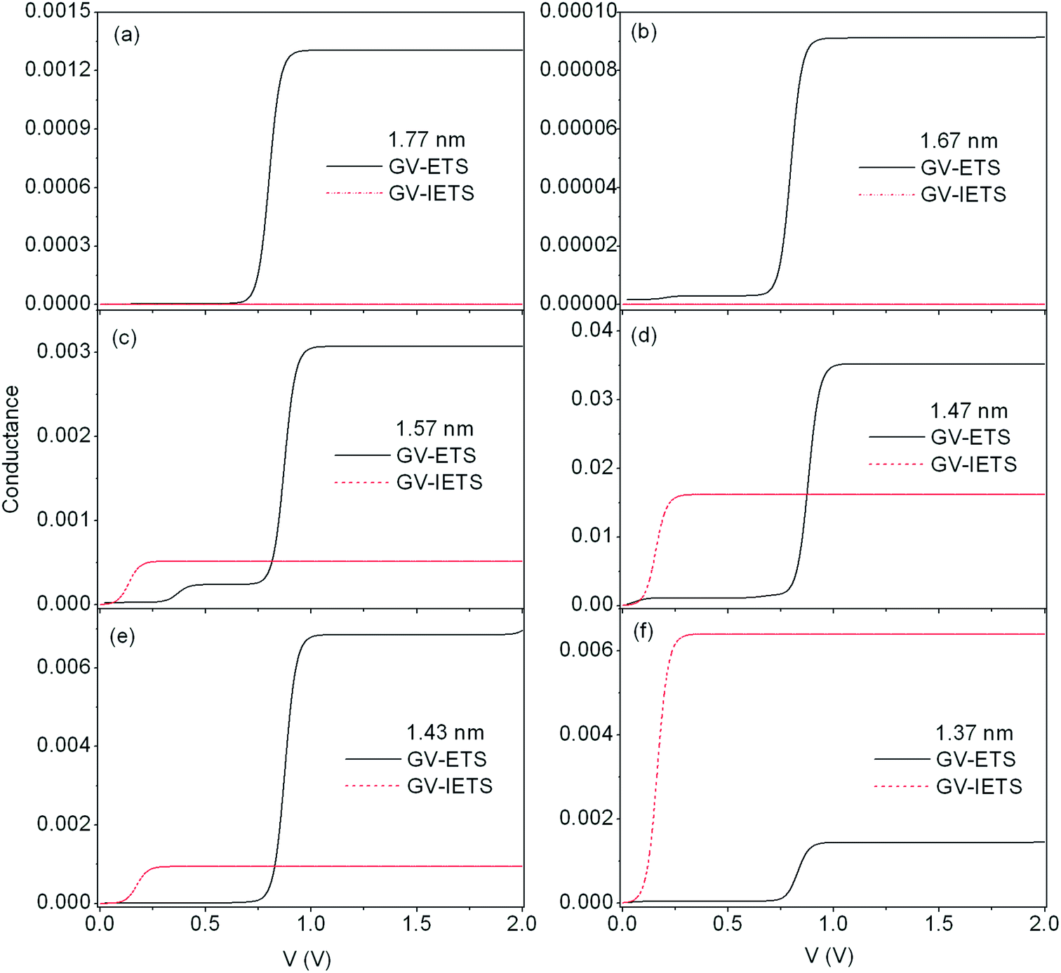 | ||
| Fig. 2 The elastic and inelastic quantum conductance (plot as G/G0 with G0 = 2e2/h being the conductance quantum, bias voltage = 2 V) curves of curved 4 × 4 GNR-based junctions with different dSD. | ||
From Fig. 2 one can clearly see that the intensity of quantum conductance is sensitive to the atom structure of central molecular core, while the positions of quantum conductance stairs appear at same energy region. Based on the junction models, the coordinate of the Au atoms have been fixed (that is, there is a certain dSD for each system) and the atoms of molecular core are fully relaxed in the geometry optimization process. Our previous results obtained that the curvature radius of the atomic plane is increased, and the deformation energy is decreased with the stretching of dSD. When dSD is larger than 1.67 nm, the curvature radius becomes very large and the deformation energy keeps as a constant.33 Comparing with the elastic conductance, the contributions of the inelastic conductance increase obviously when dSD decreasing. The inelastic conductance can be negligible for the large dSD systems (plane GNR slices) as shown in Fig. 2(a) and (b). For the small dSD systems (curved GNR slices), the contributions of inelastic conductance become comparable to the elastic conductance, as shown in Fig. 2(c) to (e). It is need to mention that the main contribution for the total conductance comes from the inelastic electron scattering in systems with small curvature radius, such as dSD = 1.37 nm system shown in Fig. 2(f). The reason may that the curvature of the GNR slices causes the hybridization of the electrons changed, and the nuclear motion for the curved systems is much stronger than that of the plane systems. The nuclear motion can introduces vibrational excited states which contribute to the inelastic electron scattering. These two mechanisms can tune the molecular orbitals and thus change the quantum conductance. From Fig. 2, one also sees that there are some differences on the magnitude of conductance. Fixed the coordinate of source drain electrodes in the optimization process, equivalent to apply stress to the GNR plane, which cause the atomic plane become curved, thus the electronic properties of the system and the transport properties of the junctions will be tuned. Furthermore, the coupling between electrodes and molecule core will also have effect on the transport properties. The proportion of elastic and inelastic component of the total current can provide a referential reflection of the localized curvature information for the GNR slices.
The inelastic electron tunneling spectroscopy of curved 4 × 4 GNRs-based junctions
Inelastic electron tunneling spectroscopy is a powerful spectroscopic tool for molecular identification and chemical bonding investigations. In this part, we studied the inelastic electron scattering properties of several 4 × 4 GNR-based molecular devices. The calculated IETS (dSD from 1.37 nm to 1.77 nm) are illustrated as a function of applied bias in Fig. 3. The shape of the calculated IETS curve agrees well with each other, while the peak positions are different. Generally, the amplitude of the IETS peak for the curved GNR-based junctions has blue-shift with decreasing the dSD. That is, with the atomic plane become more curved, vibrational energy states appear at larger energy region. With the dSD become smaller, the curvature radius become smaller and the coupling between Au atoms and carbon atoms become stronger. When the dSD become much smaller, the strong coupling may constraint the nuclear motion partially, thus, the blue-shift effect cannot be seen for the dSD = 1.37 nm system. For the dSD = 1.77 nm system, the molecular core keeps plane atomic structure and the overlap between Au atoms and edge passivated hydrogen atoms and sub-edge carbon atoms can be negligible. There are a quite small IETS peak appears at low energy regions. One can conclude that the electron inelastic scattering of the curved GNR-based junctions are orders of magnitude stronger than that of the plane ones. The large difference in the spectral intensity and distributions related to the molecular vibrational modes implies that the molecular conformations and the connection of molecular core and electrodes are different. | ||
| Fig. 3 The inelastic electron tunneling current as function of source-drain bias voltage of the curved GNR-based molecular devices with different dSD. | ||
The temperature dependences of inelastic electron scattering for curved 4 × 4 GNRs-based junctions
As we all know, temperature have a profound impact on the electron scattering process. Based on the theoretical calculation methods used by the QCME code, we can find that there are two main factors closely related to temperature, one is the population distribution of thermal particles (the molecular vibrational mode has been used to describe the atomic motion in this method) which can be calculated using the Boltzmann distribution function Pn. The other is the electron Fermi distribution at the end of source and drain electrodes f(E), where , source
  and drain
  .
.
Both of the two factors have exponential dependence on temperature. The effect of Boltzmann distribution function on the tunneling current is only valid in the low frequency range. For the Fermi distribution, the energy difference is often close to zero in the vicinity of the conducting orbits, thus the effect of Fermi distribution on the tunneling current is persistent.
In order to examine the dependence of the IETS on the temperature, we choose two extended molecules with dSD = 1.57 nm and dSD = 1.77 nm as example for simplicity. The calculated inelastic electron tunneling spectroscopy under different working temperatures for the dSD = 1.57 nm system and inelastic electron tunneling current (on a log scale) under different temperature for the dSD = 1.57 nm and dSD = 1.77 nm system are shown in Fig. 4, respectively. Our calculated results shown that there is a peak of IETS in the low-frequency regions below 50 mV for curved-GNR based systems. The intensity of this peak is very small. While for the plane-GNR based systems with a large value of dSD, the molecular vibrational level appear until 100 mV. It can be seen that the IETS curve of dSD = 1.57 nm system have significant temperature dependence between 100 mV and 200 mV. From Fig. 4 (a) to (f), one can see that the peak has a significant broadening with the increase of temperature. Fig. 4 (g) shows that in the low-frequency region below 50 mV, the inelastic current curve for the dSD = 1.57 nm system is very insensitive to temperature. There are obvious changes of the inelastic current curves near 140 mV for the dSD = 1.57 nm and dSD = 1.77 nm systems as shown in Fig. 4 (g) and (h). Due to the influence of molecular vibrational modes, a new conductance level has been introduced. With the increasing of temperature, the spectral width becomes lager and lager. Until a certain temperature, the fine structure of the spectroscopy will be covered up. The high-frequency vibration modes are mainly from the contribution of the molecules. The metal atoms considered in the extended molecules will bring many low frequency vibration modes which usually derived from the metal atoms or metal–molecule vibration. In the low-energy region, the population distribution of thermal particles has a strong effect even at low temperatures. Almost all of the vibration information will be shadowed. Thus, the changes of inelastic current below 50 mV for the dSD = 1.77 nm system as shown in Fig. 4 (h) are mainly caused by the population distribution of thermal particles. One can thus conclude that the effect of temperature dependence of population distribution of thermal particles is relatively obvious in the low-frequency area. And the temperature dependence effect of IETS is mainly introduced by the Fermi distribution function. The difference in the spectral intensity distribution and temperature dependence related to the molecular vibrational modes implies that the molecule–electrodes coupling and degree of curvature of the two systems are different. It is necessary to mention that when the curvature of the GNR slice become very large such as the dSD = 1.37 nm system, the inelastic scattering become much high, the equilibrium distributions assumption should be corrected and developed. The local thermodynamic equilibrium assumption still can be used for the contacts, while for the molecular core of the junction the effect of proper non-equilibrium phonon population needs to be considered.34
 | ||
| Fig. 4 (a)–(f) The inelastic electron tunneling spectroscopy under different working temperatures for the dSD = 1.57 nm system. (g) and (h) Calculated inelastic electron tunneling current (on a log scale) under different working temperature for the dSD = 1.57 nm and dSD = 1.77 nm system, respectively. | ||
Conclusions
In this paper, the 4 × 4 finite-sized GNR slices are chosen as the prototype structure. In order to understand how the effect of curvature and temperature on the electronic structure and inelastic transport properties of finite-sized curved-GNR slices, several junctions with different dSD have been considered. We focus on the electron inelastic tunneling spectroscopy. Comparing with the elastic conductance, the contributions of the inelastic conductance increase obviously when dSD increasing. The inelastic conductance can be negligible for plane GNR slices based junctions. For the curved GNR slices based junctions, the contributions of inelastic conductance become comparable to the elastic conductance. The electron inelastic scattering of the curved GNR-based junctions are orders of magnitude stronger than that of the plane ones. The effect of temperature dependence of population distribution of thermal particles is relatively obvious in the low-frequency area. And the temperature dependence effect of IETS is mainly introduced by the Fermi distribution function. From practical applications point of view, for one hand the curvature and temperature dependence of the elastic and inelastic current for the finite-sized GNR based junctions can provide a referential reflection of the localized curvature information for the GNR slices, for the other it have probable applications in molecular microprobes.Acknowledgements
This work was supported in part by the National Natural Science Foundation of China (11304001, 51272001, 51472003 and 11174002), the National Key Basic Research Program (2013CB632705), the Ph.D. Programs Foundation for the Youth Scholars of Ministry of Education of China (20133401120002), the Foundation of State Key Laboratory for Modification of Chemical Fibers and Polymer Materials Donghua University (LK1217), the Foundation of Co-operative Innovation Research Center for Weak Signal-Detecting Materials and Devices Integration Anhui University (01001795-201410), the Key project of the Foundation of Anhui Educational Committee (KJ2013A035) and the Ph.D. Programs Foundation of Anhui University (33190134). Computational resources from the Shanghai Supercomputer Centre are acknowledged.Notes and references
- Y. Q. Xue and M. A. Ratner, Phys. Rev. B: Condens. Matter Mater. Phys., 2004, 69, 085403 CrossRef.
- R. Cohen, K. Stokbro, J. M. L. Martin and M. A. Ratner, J. Phys. Chem. C, 2007, 111, 14893–14902 CAS.
- Y. Xu, Z. Lin, X. Huang, Y. Liu, Y. Huang and X. Duan, ACS Nano, 2013, 7, 4042–4049 CrossRef CAS PubMed.
- S. W. Seo, E. Jung, S. J. Seo, H. Chae, H. K. Chung and S. M. Cho, J. Appl. Phys., 2013, 114, 143505 CrossRef PubMed.
- X. W. Wang, G. Z. Sun, P. Routh, D. H. Kim, W. Huang and P. Chen, Chem. Soc. Rev., 2014, 43, 7067–7098 RSC.
- K. S. Mali, J. Greenwood, J. Adisoejoso, R. Phillipson and S. D. Feyter, Nanoscale, 2015, 7, 1566–1585 RSC.
- Y. H. Wang, K. Bian, C. G. Hu, Z. P. Zhang, N. Chen, H. M. Zhang and L. T. Qu, Electrochem. Commun., 2013, 35, 49–52 CrossRef CAS PubMed.
- S. Das, P. Sudhagar, Y. S. Kang and W. Choi, J. Mater. Res., 2014, 29, 299–319 CrossRef CAS.
- J. H. Lee, J. Y. Tan, C. T. Toh, S. P. Koenig, V. E. Fedorov, A. H. C. Neto and B. Ozyilmaz, Nano Lett., 2014, 14, 2677–2680 CrossRef CAS PubMed.
- M. A. Bissett, M. Tsuji and H. Ago, Phys. Chem. Chem. Phys., 2014, 16, 11124–11138 RSC.
- H. H. Pu, S. H. Rhim, C. J. Hirschmug, M. Gajdardziska-Josifovska, M. Weinert and J. H. Chen, Phys. Rev. B: Condens. Matter Mater. Phys., 2013, 87, 085417 CrossRef.
- K. S. Kim, Y. Zhao, H. Jang, S. Y. Lee, J. M. Kim, K. S. Kim, J. H. Ahn, P. Kim, J. Y. Choi and B. H. Hong, Nature, 2009, 457, 706–710 CrossRef CAS PubMed.
- J. G. Kushmerick, J. Lazorcik, C. H. Patterson, R. Shashidhar, D. S. Seferos and G. C. Bazan, Nano Lett., 2004, 4, 639–642 CrossRef CAS.
- W. Wang, T. Lee, I. Kretzschmar and M. A. Reed, Nano Lett., 2004, 4, 643–646 CrossRef CAS.
- L. H. Yu, Z. K. Keane, J. W. Ciszek, L. Cheng, M. P. Stewart, J. M. Tour and D. Natelson, Phys. Rev. Lett., 2004, 93, 266802 CrossRef CAS.
- A. H. Flood, J. F. Stoddart, D. W. Steuerman and J. R. Heath, Science, 2004, 306, 2055–2056 CrossRef CAS PubMed.
- J. Jiang, M. Kula, W. Lu and Y. Luo, Nano Lett., 2005, 5, 1551–1555 CrossRef CAS PubMed.
- M. Grobis, K. H. Khoo, R. Yamachika, X. H. Lu, K. Nagaoka, S. G. Louie, M. F. Crommie, H. Kato and H. Shinohara, Phys. Rev. Lett., 2005, 94, 136802 CrossRef CAS.
- C. F. Hirjibehedin, C. P. Lutz and A. J. Heinrich, Science, 2006, 312, 1021–1024 CrossRef CAS PubMed.
- M. Kula, J. Jiang, W. Lu and Y. Luo, J. Chem. Phys., 2008, 128, 064705 CrossRef PubMed.
- M. Paulsson, T. Frederiksen and M. Brandbyge, Nano Lett., 2006, 6, 258–262 CrossRef CAS PubMed.
- J. Lykkebo, A. Gagliardi, A. Pecchia and G. C. Solomon, ACS Nano, 2013, 7, 9183–9194 CrossRef CAS PubMed.
- M. Paulsson, T. Frederiksen, H. Ueba, N. Lorente and M. Brandbyge, Phys. Rev. Lett., 2008, 100, 226604 CrossRef.
- A. Troisi and M. A. Ratner, Nano Lett., 2006, 6, 1784–1788 CrossRef CAS PubMed.
- G. C. Solomon, A. Gagliardi, A. Pecchia, T. Frauenheim, A. D. Carlo, J. R. Reimers and N. S. Hush, J. Chem. Phys., 2006, 124, 094704 CrossRef PubMed.
- A. D. Becke, J. Chem. Phys., 1993, 98, 5648–5652 CrossRef CAS PubMed.
- C. Lee, W. Yang and R. G. Parr, Phys. Rev. B: Condens. Matter Mater. Phys., 1988, 37, 785–789 CrossRef CAS.
- J. Jiang, C. K. Wang and L. Yi, Quantum chemistry for molecular electronics, QCME-V1.1 Search PubMed.
- C. K. Wang and Y. Luo, J. Chem. Phys., 2003, 119, 4923–4928 CrossRef CAS PubMed.
- J. Jiang, M. Kula and Y. Luo, J. Chem. Phys., 2006, 124, 034708 CrossRef PubMed.
- A. Troisi, M. A. Ratner and A. Nitzan, J. Chem. Phys., 2003, 118, 6072–6082 CrossRef CAS PubMed.
- M. Galperin, M. A. Ratner and A. Nitzan, J. Phys.: Condens. Matter, 2007, 19, 103201 CrossRef.
- Z. L. Ding, J. Jiang, H. B. Shu, X. S. Chen and W. Lu, J. Nanosci. Nanotechnol., 2011, 11, 1–4 CrossRef PubMed.
- A. Gagliardi, G. Romano, A. Pecchia, A. D. Carlo, T. Frauenheim and T. A. Niehaus, New J. Phys., 2008, 10, 065020 CrossRef.
| This journal is © The Royal Society of Chemistry 2015 |