
 Open Access Article
 This Open Access Article is licensed under a
 Creative Commons Attribution 3.0 Unported Licence
Stable negative differential resistance in porphyrin based σ–π–σ monolayers grafted on silicon†
Kavita
Garg
a,
Chiranjib
Majumder
b,
Shiv Kumar
Gupta
c,
Dinesh Kumar
Aswal
c,
Sandip Kumar
Nayak
a and
Subrata
Chattopadhyay
*a
aBio-Organic Division, Bhabha Atomic Research Centre, Mumbai, 400085, India. E-mail: schatt@barc.gov.in
bChemistry Division, Bhabha Atomic Research Centre, Mumbai, 400085, India
cTechnical Physics Division, Bhabha Atomic Research Centre, Mumbai, 400085, India
First published on 1st June 2015
Abstract
Two Si-based hybrid self-assembled monolayers were synthesized by electro-grafting two di-O-alkylated porphyrins as the σ–π–σ systems. The monolayers showed a stable and reversible negative differential resistance (NDR) property at room temperature. The monolayer, fabricated using the porphyrin with fluorophenyl groups was more compact and showed a tenfold peak-to-valley ratio (PVR) relative to the other similar system devoid of the fluorine atoms in the porphyrin moiety. This suggested better pre-organization of the former, possibly by hydrogen bonding through the electro-negative fluorine atoms.
Introduction
Extensive research is being carried out on electron-transfer (ET) processes through molecular scaffolds due to their potential technological applications in molecular electronic devices.1 Studies have demonstrated that besides the junction geometry, the structures of the incorporated molecules also dictate the electron-transfer rates, current–voltage (J–V) curves and the behaviour of the resulting devices.2a–g Self-assembled systems of organic molecules on metal/semiconductor substrates, prepared by Langmuir–Blodgett (LB) films, or chemically-grafted monolayers of organic molecules junction is a powerful ‘bottom-up’ approach for the fabrication of devices for molecular-scale electronics.3 Integration of molecular components into electronic circuits by grafting on Si is expected to miniaturize the electronic circuits to nanoscale.4 This approach offers the advantage of tailoring the surface potential for improved hybrid molecular devices, changing the p-n junction threshold voltage by adjustment of the electronic nature and/or use of multiple oxidation states of the organic π group molecules, instead of classical doping of silicon.5 The negative differential resistance (NDR) behavior (i.e., an initial rise in current and its subsequent sharp drop even with progressively augmented voltage, as opposed to Ohm's law) has drawn significant attention because of its potential application in realization of logic devices and memory circuits,2b,6 and is found in a variety of molecular devices.4b,7 NDR effects have been reported using various organic molecules and different types of junctions. Some representative examples include (i) boron doped Si (111) surfaces,8a,b diamond films,8c and thiols on Au surfaces (all at room temperature),8d (ii) 2′-amino-4,4′-di(ethynylphenyl)-5′-nitro-1-benzenethiol, sandwiched between two metal electrodes (observed at 60 K),2b (iii) Pd/ferrocene self-assembled layer/Au structure,8e (iv) cyclopentene molecules, deposited on p-type hydrogen free Si(001) (observed at 80 K),2b (v) styrene and 2,2,6,6-tetramethyl-1-piperidinyloxy, deposited on degenerately doped Si (100) reconstructed surfaces,8f and (vi) disulfide molecules deposited on Si.8g In an interesting study, organic molecules deposited on doped Si (100) surfaces by ultrahigh vacuum scanning tunnelling microscope (STM) showed room temperature NDR behaviour that was decided by the nature of the molecules and the dopants.8h In all these cases, the resonant and off-resonant electronic tunneling mechanism provide satisfactory explanations for the NDR behavior.9 A large peak-to-valley ratio (PVR) in the NDR effect, required for fast switching and functioning of the device at room temperature with high reproducibility are the prerequisites for applications in hybrid nanoelectronics. Most of the reported molecular hybrids, exhibiting the NDR behaviour did not fulfil many of these criteria, and the measurements were carried out under ultra-high vacuum in certain cases. Some of the devices were made using expensive techniques such as STM, and require appropriate biasing and doping. Due to the variation of the electronic structures of the STM tips during experimentation, NDR may occur at different bias magnitudes and polarities. Also, routine impurity doping is problematic due to uncertainty of its distribution.10Thus, despite impressive progress in molecular electronics, search for alternate single molecules or a finite ensemble of self-assembled molecules showing NDR property at a lower bias is currently an active research area in molecular electronics. Amongst the electron-rich organic molecules, porphyrins11 are used extensively in fabricating molecular devices because they (i) form stable π-cation radicals, and exhibit two accessible cationic states in monomeric forms;12a–e (ii) have long charge retention times, hence less power consumption, (iii) are highly stable,12f and (iv) can form self-assembled structures.12g Despite all these attributes and theoretical proposition,8h,13 scarce attention has been paid to construct porphyrin-based NDR devices experimentally. Previously, the J–V curves of some porphyrin-metal ions combinations showed NDR-like effect.14a–c We have also found electrical bistability and current rectification properties of some porphyrin monolayers on Si surfaces.14d,e More recently, metal-free and Zn-bis-porphyrin molecules have been used as efficient chemosensors for Cl2 and NH3 gases in air.15 Presently, we fabricated redox-active porphyrin monolayers on Si and investigated the possibility of using the oxidation states of the porphyrin molecules as molecular-scale information storage systems. The prime aim was to develop devices that are environmentally stable, and show high repeatability and easy processability. Studies on the J–V characteristics of the hybrid systems revealed stable, reversible, reproducible, and room temperature NDR behaviour by both the systems. We also demonstrate that the NDR property can be tuned by subtle changes in the porphyrin structure by incorporating an electro-negative substituent (F) at the meso-phenyl groups.
Results and discussions
Given the importance of the molecular bridges in nano-devices, design of the organic molecule is crucial in attaining our objectives. The molecular design was conceived keeping in mind that the energy gap (ΔE) between the energy states (LUMO/HOMO) of the molecular bridges and the Fermi levels of the donor and acceptor units control the electron-transfer rate and current flow.16 For large ΔE, the ET process is dominated by a “through-bond” non-resonant tunnelling mechanism, where the organic molecules generally act as poor electron conductors. However, alteration of their electronic structures can induce the ET process via a resonant tunnelling or a hopping mechanism. The change from a non-resonant to resonant tunnelling would result in an abrupt increase in the current, and the measured J–V curves would show NDR characteristics.17 Resonant tunnelling requires a double potential barrier along the electron transfer coordinates. Earlier, we have proposed a possible physical origin for such a double potential barrier, and hypothesized that the σ–π–σ monolayers, grafted on Si might show NDR effect.14d The σ–π–σ molecular architecture is analogous to the tunnel diode, with a ‘quantum well’ surrounded by thin layer barriers.18 Here, the π-moiety (a conjugated molecule) acts as a quantum well and the σ-moieties (alkyl chains) as the tunnel barriers. The NDR effect in such a monolayer is expected, if electrons tunnel through some resonant states of the π-moiety. Our previous studies with N-(2-(4-diazoniophenyl)ethyl)-N′-hexylnaphthalene-1,8,4,5 tetracarboxy diimide tetrafluoroborate as a σ–π–σ molecule showed poor NDR effect (PVR ∼ 10) with hysteresis, but established the hypothesis.19 Hence, we synthesized two new di-O-alkylatedporphyrins 5a and 5b with tetraphenylporphyrin (TPP) and a fluoro-TPP derivatives as the respective quantum wells (π moiety), and a C6-alkyl chain and a C11-alkenyl chain as the barriers. The choice of the alkenyl chain as one of the barriers was a part of the molecular design, because this helped in electro-grafting monolayers of the molecules on Si (111) surfaces. Subsequently, the possibility of using the oxidation states of the porphyrin molecules as molecular-scale devices was investigated using the fabricated porphyrin–Si hybrids.Synthesis of porphyrins 5a and 5b
The classical one-pot method of Adler and Longo involving an acid-catalyzed reaction between pyrrole and an aryl aldehyde under refluxing conditions is suitable for the synthesis of symmetric (A4-Por) or partially symmetric (A3B-Por) porphyrins, where A and B are the meso-aryl substituents.20a Extension of the method to synthesize porphyrins, bearing two or more types of meso-substituents provides a statistical mixture of six porphyrins from which isolation of pure compounds becomes extremely difficult. Hence, we adopted Lindsey's method involving a “2 + 2” route using a dipyrromethane-1,9-dicarbinol and a dipyrromethane (bearing ABC- and D-substituents, respectively) for the synthesis of the target porphyrins 5a and 5b.20b This involved a base-catalyzed alkylation of 4-hydroxybenzaldehyde with 1-bromohexane and 11-bromoundec-1-ene to furnish the aldehydes 1a and 1b respectively. The aldehydes were individually subjected to a trifluoroacetic acid (TFA)-catalyzed condensation with pyrrole to yield the dipyrromethanes 2a and 2b respectively. Compound 2a was subsequently acylated with benzoyl chloride (3a) or 4-fluorobenzoyl chloride (3b) using EtMgBr as the base to afford the ketones 4a and 4b respectively. This reaction is tricky and produces both mono- and di-acylated products if the stoichiometry and reaction temperature are not maintained carefully. The ketones 4a and 4b were subsequently reduced with NaBH4 and the resultant unstable diols were converted to the porphyrins 5a and 5bvia a TFA-catalyzed condensation with 2b followed by a 2,3-dichloro-5,6-dicyano-1,4-benzoquinone (DDQ) oxidation, the three-steps process being carried out in one-pot (Scheme 1).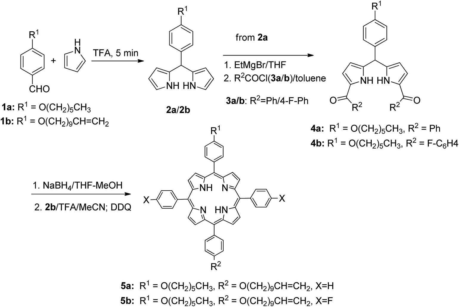 | ||
| Scheme 1 Syntheses of the prophyrins. | ||
Preparation of the grafted organic assembly
Physisorption of organic molecules as Pockels–Langmuir (PL) films or by vapor-phase deposition on electrodes is often used to fabricate hybrid organic electronic devices. However, ordering of PL films is usually achievable with amphiphilic molecules only, restricting the molecular design. On the other hand, the vapor-phase deposition method often results in poor deposition yields, disordered packing and random orientations. Further, the physisorbed molecules often move to seek a lower energetic state on the surface, or in response to an applied electric field. Instead, covalent linking of organic molecules to metal/semiconductor surfaces provides a better alternative.21 Extensive work has been carried out by attaching organic thiol molecules to Au electrodes. But, the Au surfaces are reported to be thermally unstable.22 Monolayers of alkyl silanes have been grafted on SiO2 surface, but the multi-steps protocol required stringent reactions conditions such as control of the optimized temperature and anhydrous conditions. In addition, many of the alkyl silanes have to be synthesized separately.23 Hence, we followed electro-grafting for an easy attachment of the porphyrins on Si (111) surface through the strong Si–C bond (Si–C ∼76 kcal mol−1).23b Organic molecules having a cleavable group such as vinyl (C![[double bond, length as m-dash]](https://www.rsc.org/images/entities/char_e001.gif) C), ethynyl (C
C), ethynyl (C![[triple bond, length as m-dash]](https://www.rsc.org/images/entities/char_e002.gif) C), halide (Cl, Br, I), tetraalkylammonium, and diazonium silane reacts with H-terminated Si, and can be deposited using electrografting process. The advantage of the process is that the deposition process can be monitored in situ by measuring the redox peak of the electrografting reaction.
C), halide (Cl, Br, I), tetraalkylammonium, and diazonium silane reacts with H-terminated Si, and can be deposited using electrografting process. The advantage of the process is that the deposition process can be monitored in situ by measuring the redox peak of the electrografting reaction.
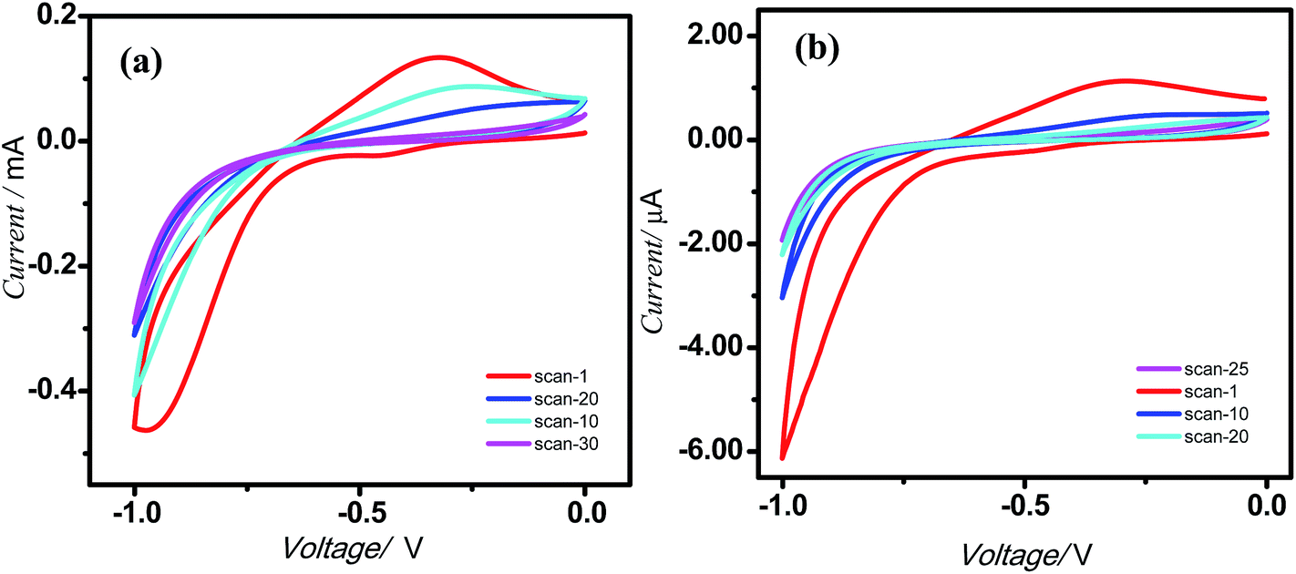
Presently electrografting of the molecules 5a and 5b on highly-doped, commercially available Si (111) surfaces was achieved by conventional cyclic voltammetry (CV). The CVs (Fig. 1), recorded during electrochemical deposition of the molecules 5a and 5b on Si showed an irreversible peak at ∼0.3 V, which was earlier assigned for the bonding of an alkene with the H-terminated Si surfaces.14d Moreover, no peak at 0.3 V appeared when the CV was run using the TBAP solution alone, but similar peak was observed with 1-undecene (taken as reference). This indicated covalent attachment of the porphyrin molecules at the H-terminated Si surfaces is through terminal double bond. The possible electrochemical reactions in the process is schematically shown in ESI (Fig. SL1†). In the first step, application of a negative potential to the working electrode produces a radical on silicon and a proton. The Si radical subsequently reacts with the alkene function of 5a and 5b to form the Si–C bond, and generates a C-centred radical β to the Si atom. A subsequent transfer H atom from another Si–H bond generates a new Si radical to propagate the process. Formation of the Si–C bond resulted in the irreversible oxidation peak at ∼0.3 V. As the number of scans increased, the peak diminished owing to the non-availability of nucleophilic Si atoms at the surface. Using different number of scans (5, 10, 20, 25 and 30), a compact monolayer, as revealed by AFM (Fig. 2) was prepared at 25 and 30 scans respectively with 5a and 5b. At higher scans, formation of multilayers was evident by AFM analysis (data not shown).
 | ||
| Fig. 1 CVs indicating electrografting of the molecules on silicon (n++) wafers. (a) 5a; (b) 5b. The deposition was carried out under N2 atmosphere at a scan rate of 0.05 V s−1 using Si wafers as the WE, Pt as the CE, Ag/AgCl as the RE, 0.1 M Bu4NP as the electrolyte and the porphyrins (1 μM) in dry CH2Cl2. | ||
 | ||
| Fig. 2 AFM images (1 μm × 1 μm) for the monolayers of (a) 5a; (b) 5b, electro-grafted on silicon (n++) wafers. | ||
Monolayer characterization
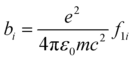
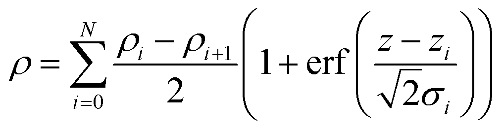
In order to ascertain the monolayer deposition on Si, the electro-grafted materials were characterized by contact angle measurement, polarized FT-IR spectroscopy, X-ray reflectivity (XRR), ellipsometry, AFM, secondary ion mass spectrometry (SIMS) and electrochemistry. The contact angles of deionized water in case of Si wafers, grafted with 5a and 5b were ∼58° and 64° respectively, whereas for the cleaned Si wafer it was 84°. The observed contact angles were much less than the reported values (97–108°) of the methyl terminated alkyl chains.24 This suggested interaction of the water molecule with the porphyrins, possibly through their pyrrole rings, which is possible only when the molecules are tilted. This was also confirmed by ellipsometry, where the average thicknesses of respective monolayers were found to be ∼2.3 ± 0.2 nm in case of 5a and 2.9 ± 0.2 nm with 5b. The XRR experiments, carried out at room temperature with the monolayers further confirmed their thicknesses. The reflectivity data (Fig. 3) was fitted in MOTOFIT software, using Parratt's formalism. The scattering length density (SLD) values of the monolayers were calculated from the density of monolayer and molecular formula of molecule according to eqn (1).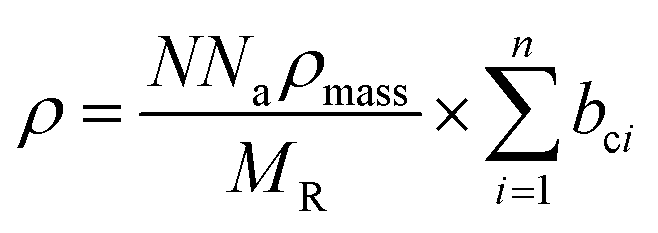 | (1) |
 | (2) |
 | (3) |
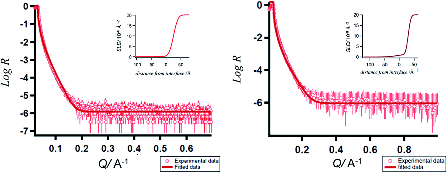 | ||
| Fig. 3 XRR curves of the porphyrins-grafted monolayers on silicon (n++) wafers. (a) 5a; (b) 5b; insets: SLD plots. | ||
From the plot of SLD vs. interface distance, the thicknesses for 5a and 5b were found to be 2.54 ± 0.02 nm and 3.05 ± 0.03 nm respectively (Fig. 3 inset). These values are lower than the theoretically calculated (using Molkel software) length ∼3.9 nm of the porphyrins. The roughness values for the monolayers of 5a 24.0 Å (SLD = 0.22 × 10⁻⁶ Å−2, χ5a2 = 0.04913) and 5b 29.7 Å (SLD = 2.23 × 10⁻⁶ Å−2χ5a2 = 0.03049) were close to their thicknesses estimated by ellipsometry. The XRR data also indicated that the tilt angles of the monolayers were ∼39° and 51.4° for 5a and 5b respectively.
The AFM analyses revealed that the monolayers were more organized with lesser number of voids and hillocks, and the void depths were ∼2.3 nm for 5a and 2.9 nm for 5b (Fig. 2). The RMS and average roughnesses values of the monolayers were 1.45 and 1.16 nm for 5a, and 0.89 and 0.73 nm for 5b. Compared to 5a, the monolayers of 5b were more compact and uniform with larger grain size. The fast scan (10 V s−1) CVs (Fig. 4) of the monolayers exhibited a reversible peak at +0.8 V for the respective porphyrin moieties and no such peak was observed in bare silicon and undecene deposited silicon. The net charge transferred during the oxidation process, calculated from the area under the oxidation peak were 4.5 × 10⁻⁸ C and 8.8 × 10⁻⁷ C respectively for 5a and 5b. These amounted to surface coverages of 4.3 × 10¹¹ and 3.4 × 10¹² molecules cm−2 respectively for 5a and 5b. Thus, the surface covered by 5b was ∼8 times that by 5a. These data are consistent with the AFM analyses, both revealing more compact monolayers with 5b than 5a. This may be because of hydrogen bonding amongst the F and H atoms of the porphyrin phenyl moieties.
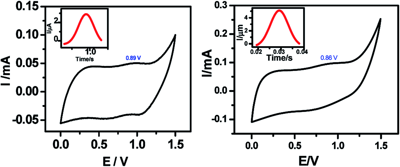 | ||
| Fig. 4 Fast scan CVs for the monolayers of (a) 5a; (b) 5b; electro-grafted on silicon (n++) wafers. The CVs were recorded under N2 atmosphere at a scan rate of 10 V s−1 using the respective monolayer-grafted Si as the WE, Pt as the CE and Ag/AgCl as the RE, and 0.1 M Bu4NP as the electrolyte. The reversible peaks are indicated by circles. Insets show the magnified redox peaks, after background correction and converting the potential scale into time scale. | ||
Identifying the C–H/F–C interaction as a hydrogen bond is questioned due to the poor acceptor ability of C-bonded F atoms compared to the O- and N-atoms, if present.26 However, distinct hydrogen bond character has been reported in the layered crystal structure of fluoroaromatics, where C–H/F–C interactions contribute significantly in stabilizing the layers. This has been attributed to activation of the ortho-aromatic protons by the F atom that may override the poor acceptor nature of the C-bonded halogen.27 In addition, the face-to-face noncovalent interaction in arene–perfluoroarene system is ubiquitous, and widely recognised as one of the major driving forces in forming robust supramolecular assemblies.28 This primarily involves stabilizing Coulombic interactions, and has been reported with several fluoroaromatic compounds.29 In the present case, the parallel offset disposition of the fluorophenyl moieties of adjacent porphyrin molecules may also be responsible for the compact monolayers of 5b.
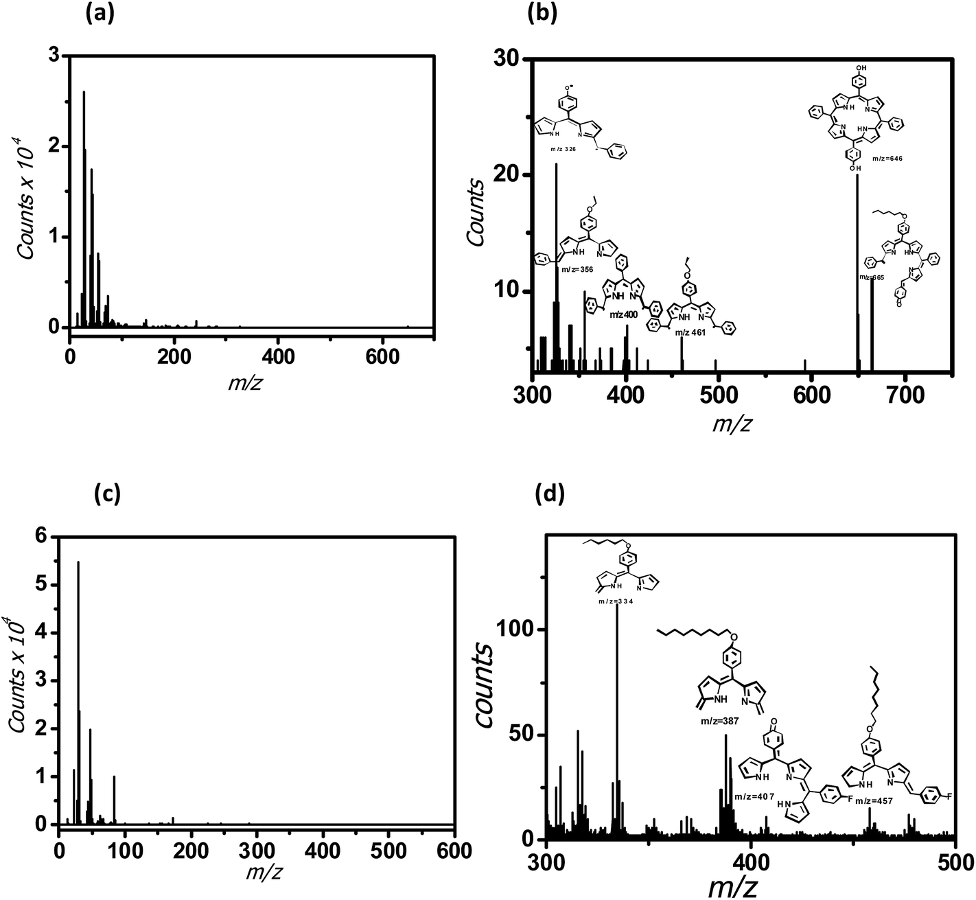
The SIMS of the monolayer of 5a showed peaks due to the porphyrin fragments at m/z 665, 646, 461, 400, 356 and 324 amu. In case of 5b, the peaks appeared at a lower mass range viz. m/z 457, 407, 387 and 334 amu. Nevertheless, the SIMS data (Fig. 5(a) and (b)) of the monolayers of 5a and 5b confirmed deposition of their respective monolayers on the Si wafers. In case of 5a monolayers, the secondary ions knocked down the porphyrin moiety from the alkyl spacer, attached to the Si surface. Subsequent ionization of the released porphyrin moiety provided the mass fragments at higher masses. Possibly, the secondary ions cannot penetrate the more compact 5b monolayers, resulting in the fragmentation of the porphyrin moiety in the middle to generate the low molecular weight mass peaks of the truncated porphyrin moiety.
 | ||
| Fig. 5 SIMS of the porphyrins-grafted monolayers on silicon (n++) wafers. (a) 5a; (b) enlarged plot for 5a; (c) 5b; (d) enlarged plot for 5b. | ||
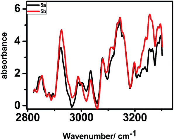
The polarized FTIR spectra (Fig. 6) for the monolayers of 5a exhibited N–H stretching frequency at 3249 cm−1, symmetric (νs) and asymmetric stretching modes (νa) of CH2 group at 2842 and 2910 cm−1 and of CH3 group at 2877 and 2949 cm−1. In contrast, the respective IR absorption peaks of the monolayers of 5b were at 3255 cm−1, 2855 and 2925 cm−1, and at 2871 and 2961 cm−1. In pure solid alkane monolayers, the hydrocarbon chains exist in an all-trans configuration such that the carbon backbone of each molecule lies in single planes. However, in liquid form, there is a substantial twisting about the individual bonds; these out-of-plane twists alter the frequency of the CH2 vibrational modes.30 Thus, the IR peaks due to the CH2 vibrational modes can provide better insights about the proposed van der Waals interactions between the porphyrin rings, parallely anchored on Si. Our IR data showed that the alkyl chains in the monolayers of 5a are more rigid like in pure solid alkanes, while that in the monolayers of 5b are more liquid like and twisted. Presumably, in case of 5b, the phenyl rings of the porphyrin moiety are more tightly packed setting the alkyl chains free to twist. But in case of 5a, proper packing requires stacking of the porphyrins as well as the alkyl moieties at a tilt angle of 39°. This rigidifies the alkyl chains in 5a.
 | ||
| Fig. 6 Polarized FTIR spectra of the monolayers of 5a and 5b on silicon (n++) wafers. | ||
I–V characteristics
Typical current voltage (I–V) curves of Hg/molecule/Si (111) wafers are shown in Fig. 7. The hybrid assemblies, prepared from 5a and 5b showed reversible NDR behaviour at room temperature with current PVRs of 10 and 100, and peak positions (voltage) at 1.18 V and 1.09 V respectively. The details of the I–V curves are shown in Table Sl1.† Interestingly majority of the devices, constructed with both the systems were stable during repetitive voltage scanning for 8 h in positive and negative bias voltages, without any reduction in current or the NDR effect. However, the reversible NDR effect showed only a marginal hysteresis. The Si-alkyl//Hg junctions, used in the studies are very stable, and exclude any possibility of penetration of Hg drops through pinholes or diffusion of mercury vapor through the SAM. Thus, the measured I–V is expected to be direct. The statistical analyses of data, and junction yields are extremely valuable to discriminate artifacts from real data.31 In the present work, we constructed 96 and 48 devices, respectively with the compounds 5a and 5b. Of these, 80 and 43 devices, made of 5a and 5b showed stable (up to 8 h), and reversible NDR property, although 94 and 46 of these devices showed reversible NDR behavior.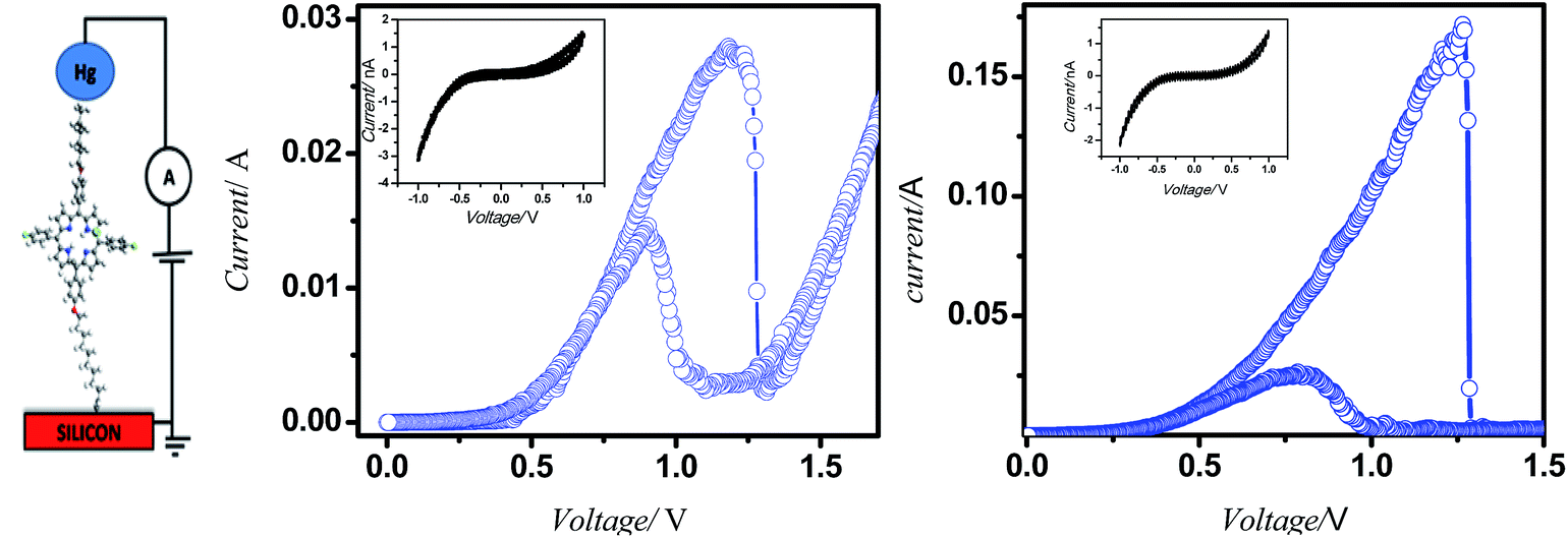 | ||
| Fig. 7 Device design and characteristics. (a) I–V measurement set up; (b) and (c) I–V plots of the monolayers of 5a and 5b on silicon (n++) wafers respectively. | ||
The complete PVR statistics of the devices are shown as the ESI (Table Sl2† and the accompanying pi-chart), and summarized here. With compound 5a, the PVR values of 36% of the devices were 8–10, while an additional 37% of the devices showed PVR values 5–8. The device statistics of the monolayers of 5b were more impressive with 39% of the devices showing PVR values of 80–100, an additional 33% with PVR of 50–80, and an additional 24% with PVR of 10–50. The I–V characteristics of the solid state devices can be understood in terms of the molecular properties observed in the solution. Presently, the current flow in both the solid-state devices (Fig. 4) as well as in the respective porphyrin solutions (Fig. 8) showed same oxidation peaks.
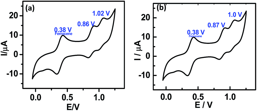 | ||
| Fig. 8 CV of the porphyrins in solution phase using ferrocene as the standard. (a) 5a; (b) 5b. | ||
The correspondence between the solution and solid-state results suggested that the fundamental molecular electronic properties of the porphyrins are retained in the solid-state devices. Hence, the forward bias current-flow should be determined by the HOMO states of the molecules, while their respective LUMO states would dictate the reverse bias current. Thus, the NDR effect in forward bias is a result of alignment of the HOMO levels of the molecules with the Fermi-levels of the electrodes. Various mechanisms such as charge transfer-induced change of the charge state, and chemical/conformational changes under finite bias have been proposed to explain NDR phenomenon.32 It is possible that presently, the NDR behaviour depends on a match (resonant tunnelling) between the Fermi levels of electrodes and the HOMO levels of molecules sandwiched between the electrodes, followed by a mismatch of HOMO levels of the oxidized molecules with the Fermi-levels of electrodes. The hypothesis is consistent with the Aviram–Ratner model of molecular rectification.4a However, involvement of additional mechanisms can't be excluded.
Theoretical interpretation
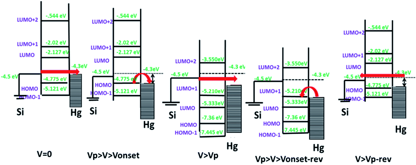
For further clarification, the theoretical calculations of the electronic transport behaviour were carried out. The ground state geometries of the molecules 5a and 5b were optimized by ab initio molecular orbital calculations. The ionic optimization of molecules 5a and 5b was carried out without any symmetry constraint at the B3LYP/6-31G (d,p) level of theory. The geometrical parameters of both molecules were found to be same, except for the C–H and C–F bond lengths, which were 1.09 Å and 1.39 Å, respectively.Our experimental results revealed that on applying voltage, initially there was a slow rise in the current due to tunnelling. But at Vonset the HOMO level of the molecule would align in resonance with the Fermi level of Hg. This can explain the sharp increase in current at Vonset. At Vp, the molecules get oxidized to the +1 state, causing the misalignment with the Fermi-levels of Hg, and resulting in the current drops. When the voltage is reduced in the reverse scan, the new device will be Si/porphyrin+1/Hg. At Vonset-rev, the Fermi level of Hg would align with the LUMO of porphyrin+1. This induces a sharp increase in the current due to resonance tunnelling through the molecule. It again drops at Vp-rev as the molecule gets misaligned with the Fermi levels of Hg during its reduction. The observed small hysteresis may be due to conformational changes in the molecule after oxidation. The experimentally observed voltages are in qualitative agreement with the theoretically calculated HOMO–LUMO values of 5a and 5b and their respective +1 oxidation states, using ab initio (GAMESS software) (data shown in ESI, Table SL3†). The mechanism of NDR effect in 5a and 5b is explained schematically in Fig. 9.
 | ||
| Fig. 9 Diagramatic presentation of the NDR mechanism for a σ–π–σ system. | ||
Conclusions
In summary, we have synthesized two di-O-alkylated porphyrin molecules as prototype σ–π–σ systems, and electro-grafted them on H-terminated Si to form monolayers. The I–V characteristics of the monolayers revealed pronounced reversible NDR effects with peak-to-valley current ratio of ∼10 and 100. The NDR effects were relatively stable during repetitive voltage scanning for 8 h in the positive and negative bias, without any reduction in current or in the NDR effect. The higher PVR, observed with the device containing the fluorophenylporphyrin moiety 5b suggested its better pre-organization possibly by hydrogen bonding through the F atoms, compared to the device, fabricated using the non-fluorinated porphyrin, 5a. Theoretical simulations of Si/porphyrin/Hg structure showed that the NDR effect is intrinsic to the porphyrin molecules. The NDR effect was explained using the ab initio molecular-orbital theoretical calculations.Experimental section
General methods in synthesis
Reagents and solvents (Sigma-Aldrich and Fluka) were of synthetic grade. Pyrrole and benzoyl chloride used after distillation. 4-Hydroxybenzaldehyde was used after crystallization. All solvents were dried and distilled before use. Tetrahydrofuran (THF) was distilled from Na under argon. Acetone was dried over Na2CO3 and HPLC grade acetonitrile was used. The 1H NMR and 13C NMR spectra were recorded with 200/300/500 (50/75/100) MHz spectrometers using deuterated solvents as the internal standards. The mass spectrometry was carried out with a MSMS (410 Prostar Binary LC with 500 MS IT PDA Detectors, Varian Inc, USA) and MALDI-TOF/TOF (BrukerUltraflex II) data systems.Compound 1a. colorless liquid; IR (film, ν/cm−1): 3019 (s), 2928 (s), 2856 (s), 1687 (s); 1H NMR (200 MHz, CDCl3): δ 0.90 (t, J = 6.4 Hz, 3H), 1.15–1.49 (m, 6H), 1.71–1.88 (m, 2H), 4.01 (t, J = 6.0 Hz, 2H), 6.97 (d, J = 9.5 Hz, 2H), 7.80 (d, J = 9.5 Hz, 2H), 9.85 (s, 1H) ppm; 13C NMR (50 MHz, CDCl3): δ 13.6, 22.2, 25.3, 28.7, 31.2, 68.1, 114.4, 129.6, 131.5, 163.9, 190.04 ppm; MSMS (m/z): 207 (100) [M + H]+; anal. calcd for C13H18O2: C, 75.69; H, 8.80. Found: C, 75.34; H, 9.06%.
Compound 1b. Colorless liquid; IR (film, ν/cm−1): 3019 (s), 2928, 2856 (s), 1687 (s); 1H NMR (200 MHz, CDCl3): δ 1.21–1.57 (m, 12H), 1.72–1.95 (m, 2H), 1.96–2.15 (m, 2H), 4.05 (t, J = 6.0 Hz, 2H), 4.85–5.08 (m, 2H), 5.67–5.99 (m, 1H), 6.99 (d, J = 8.0 Hz, 2H), 7.83 (d, J = 8.0 Hz, 2H), 9.88 (s, 1H) ppm; 13C NMR (50 MHz, CDCl3): δ 25.9, 28.9, 29.0, 29.3, 29.4, 33.7, 68.4, 114.1, 114.8, 129.9, 131.9, 139.1, 164.3, 190.6 ppm; MSMS (m/z): 275.1 (100) [M + H]+; anal. calcd for C18H26O2: C, 78.79; H, 9.55. Found: C, 79.02; H, 9.55%.
Compound 2a. White crystals; mp: 58 °C; IR (ν/cm−1): 3463 (m), 3019 (s), 2956 (s), 2859 (s), 2399 (w); 1H NMR (200 MHz, CDCl3): δ 0.92 (t, J = 6.2 Hz, 3H), 1.25–1.50 (m, 6H), 1.68–1.85 (m, 2H), 3.93 (t, J = 6.4 Hz, 2H), 5.42 (s, 1H), 5.85–5.93 (m, 2H), 6.12–6.22 (m, 2H), 6.61–6.68 (m, 2H), 6.84 (d, J = 7.8 Hz, 2H), 7.12 (d, J = 7.8 Hz, 2H), 7.89 (broad s, 2H) ppm; 13C NMR (50 MHz, CDCl3): δ 14.1, 22.7, 25.9, 29.4, 31.7, 43.4, 68.3, 107.2, 108.6, 114.8, 117.2, 129.5, 133.1, 134.2, 158.4 ppm; MSMS (CI, m/z): 321.2 (100) [M − H]+; anal. calcd for C21H26N2O: C, 78.22; H, 8.13; N, 8.69. Found: C, 78.60; H, 8.17; N 8.54%.
Compound 2b. White crystals; mp: 64 °C; IR (ν/cm−1): 3463 (m), 3019 (s), 2928 (s), 2856 (s), 2399 (w), 1639 (w); 1H NMR (200 MHz, CDCl3): δ 1.21–1.59 (m, 12H), 1.69–1.84 (m, 2H), 1.95–2.17 (m, 2H), 3.94 (t, J = 6.0 Hz, 2H), 4.85–5.09 (m, 2H), 5.43 (s, 1H), 5.65–5.98 (m, 3H), 6.10–6.21 (m, 2H), 6.65–6.74 (m, 2H), 6.85 (d, J = 8.5 Hz, 2H), 7.12 (d, J = 8.5 Hz, 2H), 7.95 (broad s, 2H) ppm; 13C NMR (50 MHz, CDCl3): δ 26.2, 29.1, 29.3, 29.5, 29.7, 33.9, 43.4, 68.3, 107.2, 108.6, 114.3, 114.9, 117.2, 129.5, 133.1, 134.2, 139.4, 158.4 ppm; MSMS (CI, m/z): 391.1(100) [M + H]+; anal. calcd for C26H34N2O: C, 79.96; H, 8.77; N, 7.17. Found: C, 79.62, H, 8.77, N, 7.26%.
![[thin space (1/6-em)]](https://www.rsc.org/images/entities/char_2009.gif) :1 mixture of diacetyl and monoacetyl derivatives of 2a. The required compounds 4a (0.532 g, 62%) and 4b (0.422 g, 46%) were obtained in pure form by triturating the oils with MeOH.
:1 mixture of diacetyl and monoacetyl derivatives of 2a. The required compounds 4a (0.532 g, 62%) and 4b (0.422 g, 46%) were obtained in pure form by triturating the oils with MeOH.
Compound 4a. Light brown powder; mp: 150 °C; IR (ν/cm−1): 3225 (m), 3017 (s), 2928 (s), 2856 (s), 1610 (s); 1H NMR (200 MHz, CDCl3): δ 0.89 (t, J = 6.5 Hz, 3H), 1.21–1.45 (m, 6H), 1.71–1.88 (m, 2H), 3.94 (t, J = 6.5 Hz, 2H), 5.60 (s, 1H), 5.91–6.05 (m, 2H), 6.52–6.66 (m, 2H), 6.88 (d, J = 6.8 Hz, 2H), 7.25–7.65 (m, 8H), 7.77 (d, J = 6.8 Hz, 4H), 11.08 (s, 2H) ppm; 13C NMR (50 MHz, CDCl3): δ 14.0, 22.6, 26.1, 29.2, 29.3, 31.8, 44.1, 68.1, 111.0, 114.9, 120.7, 128.0, 129.4, 129.7, 131.0, 131.6, 138.4, 141.1, 158.6, 184.4 ppm; MS (DI, m/z): 530 (100) [M]+; anal. calcd for C35H34N2O3: C, 79.22; H, 6.46; N, 5.28. Found: C, 79.04, H, 6.52, N, 5.52%.
Compound 4b. Light brown powder; mp: 120 °C; IR (ν/cm−1): 3275 (m), 3018 (s), 2932 (s), 2871 (s), 1610 (s); 1H NMR (300 MHz, acetone-D6): δ 0.87–0.93 (m, 3H), 1.21–1.38 (m, 6H), 1.68–1.82 (m, 2H), 3.99 (t, J = 6.2 Hz, 2H), 5.83 (s, 1H), 5.95–6.18 (m, 2H), 6.75–6.97 (m, 4H), 7.16–7.48 (m, 6H), 7.88–8.05 (m, 4H), 11.12 (broad s, 2H) ppm; 13C NMR (75 MHz, CDCl3): δ 13.9, 22.5, 25.7, 29.2, 31.6, 43.5, 43.9, 68.1, 111.0, 114.8, 115.0, 115.4, 120.5, 129.3, 129.5, 130.7, 131.3, 131.5, 131.7, 141.0, 158.3, 162.5, 182.9 ppm; MSMS (CIMS, m/z): 567.4 (100) [M + 1]+; anal. calcd for C35H32F2N2O3: C, 74.19; H, 5.69; N, 4.94. Found: C, 73.79, H, 5.43, N, 4.89%. The 13C–19F couplings were not analysed.
:1, 34.3 mL) was added NaBH4 (1.0 mmol) in portions. After the reduction was complete, the mixture was poured into aqueous saturated NH4Cl (60 mL) and extracted with CH2Cl2 (100 mL). The organic layer was washed with H2O (2 × 5 mL) and brine (1 × 5 mL), dried, and concentrated in vacuum to get the respective dicarbinols as foam like solids.
Mixtures of each of these compounds and dipyrromethane 2b (0.78 mmol) in CH3N (350 mL) were stirred to get a homogeneous solution. TFA (9.49 mmol) was slowly added into these under rapid stirring, followed by addition of DDQ (2.34 mmol) after 5 min. The reaction was stirred for 1 h at room temperature and then quenched with Et3N (9.49 mmol). The mixture was passed through a pad of alumina and eluted with CH2Cl2 until the eluent was colourless. The resulting solution was concentrated, passed through a pad of silica gel, and eluted with CH2Cl2 to remove the non-porphyrinic products. The purple fractions were combined and concentrated in vacuo to give the porphyrins 5a (0.069 g, 10%) and 5b (0.143 g, 20%) as purple solids, which were recrystallized from CHCl3/MeOH.
Compound 5a. Purple crystals; mp: 230 °C; IR (ν/cm−1): 3433 (s), 3019 (s), 2928 (s), 2399 (w), 1643 (w); 1H NMR (200 MHz, CDCl3): δ −2.79 (s, 2H), 0.97 (t, J = 6.6 Hz, 3H), 1.12–1.75 (m, 18H), 1.88–2.20 (m, 6H), 4.23 (t, J = 6.4 Hz, 4H), 4.82–5.08 (m, 2H), 5.75–5.98 (m, 1H), 7.21–7.38 (m, 4H), 7.61–7.79 (m, 6H), 8.02–8.28 (m, 8H), 8.78–8.96 (m, 8H) ppm; 13C NMR (50 MHz, CDCl3): δ 14.1, 22.7, 25.9, 26.2, 29.0, 29.2, 29.5, 29.6, 31.7, 33.9, 68.4, 112.8, 113.6, 113.8, 114.2, 118.7, 120.2, 130.8, 134.2, 135.6, 135.8, 138.2, 139.3, 159.1, 161.2164.5 ppm; MALDI-TOF (m/z): 882 [M]+; anal. calcd for C61H62N4O2: C, 82.96; H, 7.08; N, 6.34. Found: C, 82.94; H, 7.03; N, 6.04%.
Compound 5b. Purple crystals; mp: 225 °C; IR (ν/cm−1): 3434 (s), 3019 (s), 2927 (s), 2850 (s), 1643 (w); 1H NMR (200 MHz, CDCl3): δ −2.81 (s, 2H), 1.07 (t, J = 6.6 Hz, 3H), 1.25–1.59 (m, 18H), 1.85–2.17 (m, 6H), 4.23 (t, J = 6.0 Hz, 4H), 4.86–5.12 (m, 2H), 5.72–5.97 (m, 1H), 7.15–7.32 (m, 4H), 7.35–7.5 (m, 4H), 8.03–8.25 (m, 8H), 8.75–8.99 (m, 8H) ppm; 13C NMR (50 MHz, CDCl3): δ 14.2, 22.7, 25.9, 26.3, 29.5, 29.7, 31.7, 32.0, 68.3, 112.8, 113.6, 113.8, 118.7, 120.2, 130.9, 134.2, 135.6, 135.8, 138.2, 159.1, 161.2, 164.5 ppm; MALDI-TOF (m/z): 918 [M]+. anal. calcd for C61H60N4O2F2: C, 79.71; H, 6.58; N, 6.10. Found: C, 79.84; H, 6.64; N, 6.03%. The 13C–19F couplings were not analysed.
Preparation of H-terminated Si wafers
N-type silicon wafers (orientation: 111; resistivity: 0.001–0.005 Ωcm) and 40% NH4F were purchased from Siltronix and Fluka, respectively. The Si (111) wafers, cut into small pieces (∼0.5 cm × 1.5 cm) were cleaned by heating them in 3:1 (v/v) of conc. H2SO4:30% H2O2 (piranha) for 10 min at 80 °C. The wafers were removed, washed with excess H2O and, immersed successively in a deaerated (purged with Ar for 30 min) 40% aqueous NH4F for 10 min, and 2% aqueous HF for 2 min. The wafers were washed with deionized H2O for 1 min, dried under a stream of N2 and immediately taken into the electrochemical cell to perform the electrografting of the porphyrins 5a and 5b.
Monolayer formation
The electrochemical deposition of 5a and 5b was carried out by CV with a potentiostat/galvanostat system (model: AutolabPGSTAT 30) using the above Si wafers as the working electrode (WE), Pt as the counter electrode (CE) and Ag/AgCl as the reference electrode (RE). The solution contained 0.1 M Bu4NP as the electrolyte and 5a and 5b (1 μM) in dry CH2Cl2. The CV was run from 0 to −1 V for 25–50 cycles at 0.05 V s−1 scan rate under an inert atmosphere. It was found that homogeneous monolayer was formed at 25 scans for 5a and 30 scans for 5b. Homogeneity of monolayer was determined by AFM. After the CV scans, the WE was sonicated in CH2Cl2 for 10 min to remove the electrolyte and the unreacted or physisorbed 5a or 5b. The WE was further washed with acetone, isopropanol and methanol to obtain the respective grafted monolayers.Characterization of monolayer
The monolayers were characterized in terms of thickness, using an ellipsometer (Sentech: model SE400adv), surface morphology by AFM (Multiview 4000, Nanonics) imaging, by de-ionized water contact angle (Data Physics System, model: OCA20), FT-IR (Bruker, 3000 Hyperion Microscope with Vertex 80 FTIR System, LN-MCT 315-025 detector) in polarized ATR (20 × objective) mode for 500 scans at an angle of 45°, XRR experiments (TTRAX3 theta–theta goniometer), performed using Cu-kα as the X-ray source in a fixed monochromator mode, and molecular mass by SIMS (BARC make, Kore's Technology software). The XRR data were fitted using MOTOFIT software.33 The roughness and thickness values of the grafted layers were determined at the minimum value of χ2 for the respective monolayers. The Levenberg–Marquardt algorithm (eqn (4)) was used for obtaining the minimum value of χ2, which defines a surface in a multidimensional error space. The deepest valley in the χ2 surface signifies minimum coefficient values of the fitting function. The CV of the grafted monolayer (as WE) was recorded from 0 to 1 V for 10 cycles at a scan rate 10 V s−1.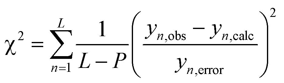 | (4) |
Junction and measurement setup
To measure the J–V characteristics, a metal/molecule/Si (n++) structure was completed by using a tiny drop of liquid mercury of diameter 400 μm as the counter electrode. The contact area in the grafted monolayer was 0.2 mm2. The J–V curves were recorded at room temperature in a dark box using a pAmeter–dc voltage source (HP 4140).Acknowledgements
One of the authors (KG) thanks Bhabha Atomic Research Centre for the financial support. The technical help by Mr A. Nelson for the MOTOFIT software is appreciated.References
- (a) B. Branchi, F. Simeone and M. Rampi, Top. Curr. Chem., 2012, 313, 85–119 CrossRef CAS PubMed; (b) C. C. Jia and X. F. Guo, Chem. Soc. Rev., 2013, 42, 5642–5660 RSC; (c) M. Ratner, Nat. Nanotechnol., 2013, 8, 378–381 CrossRef CAS PubMed; (d) D. Xiang, H. Jeong, T. Lee and D. Mayer, Adv. Mater., 2013, 25, 4845–4867 CrossRef CAS PubMed; (e) R. Lovrinčić, O. Kraynis, R. Har-Lavan, A.-E. Haj-Yahya, W. Li, A. Vilan and D. Cahen, J. Phys. Chem. Lett., 2013, 4, 426–430 CrossRef PubMed; (f) H. J. Yoon, C. M. Bowers, M. Baghbanzadeh and G. M. Whitesides, J. Am. Chem. Soc., 2014, 136, 16–19 CrossRef CAS PubMed.
- (a) M. A. Reed, C. Zhou, C. J. Muller, T. P. Burgin and J. M. Tour, Science, 1997, 278, 252–254 CrossRef CAS; (b) J. Chen, M. A. Reed, A. M. Rawlett and J. M. Tour, Science, 1999, 286, 1550–1552 CrossRef CAS PubMed; (c) E. P. A. M. Bakkers, A. W. Marsman, L. W. Jenneskens and D. Vanmaekelbergh, Angew. Chem., Int. Ed., 2000, 39, 2297–2299 CrossRef CAS; (d) R. E. Holmlin, R. F. Ismagilow, R. Haag, V. Mujica, M. A. Ratner, M. A. Rampi and G. M. Whitesides, Angew. Chem., Int. Ed., 2001, 40, 2316–2320 CrossRef CAS; (e) D. J. Wold, R. Haag, M. A. Rampi and C. D. Frisbie, J. Phys. Chem. B, 2002, 106, 2813–2816 CrossRef CAS; (f) A. Salomon, D. Cahen, S. Lindsay, J. Tomfohr, V. B. Engelkes and C. D. Frisbie, Adv. Mater., 2003, 15, 1881–1890 CrossRef CAS; (g) R. Holmlin, E. R. Haag, M. L. Chabinyc, R. F. Ismagilow, A. E. Cohen, A. Terfort, M. A. Rampi and G. M. Whitesides, J. Am. Chem. Soc., 2001, 123, 5075–5085 CrossRef CAS PubMed.
- R. M. Metzger, Acc. Chem. Res., 1999, 32, 950–957 CrossRef CAS.
- (a) A. Aviram and M. A. Ratner, Chem. Phys. Lett., 1974, 29, 277–283 CrossRef CAS; (b) C. A. Mirkin and M. A. Ratner, Annu. Rev. Phys. Chem., 1992, 43, 719–754 CrossRef CAS; (c) M. H. Dvoret, D. Esteve and C. Urbina, Nature, 1996, 379, 413–413 CrossRef.
- A. Joachim, J. K. Gimzewski and A. Aviram, Nature, 2000, 408, 541–548 CrossRef PubMed.
- J. Chen, W. Wang, M. A. Reed, A. M. Rawlett, D. W. Price and J. M. Tour, Appl. Phys. Lett., 2000, 77, 1224–1226 CrossRef CAS.
- (a) Z. Liu, A. A. Yasseri, J. S. Lindsey and D. F. Bocian, Science, 2003, 302, 1543–1545 CrossRef CAS PubMed; (b) C. Seabaugh, Y. C. Kuo and H. T. Yuan, IEEE Electron Device Lett., 1992, 13, 479–481 CrossRef; (c) D. H. Chow, H. L. Dunlap, W. Williamson III, S. Enquist, B. K. Gilbert, S. Subramaniam, P.-M. Lei and G. H. Bernstein, IEEE Electron Device Lett., 1996, 17, 69–71 CrossRef CAS; (d) Z. J. Donhauser, B. A. Mantooth, K. F. Kelly, L. A. Bumm, J. D. Monnell, J. J. Stapleton, D. W. Price, A. M. Rawlett, D. L. Allara, J. M. Tour and P. S. Weiss, Science, 2001, 292, 2303–2307 CrossRef CAS PubMed; (e) H. Inokawa, A. Fujiwara and Y. Takahashi, Appl. Phys. Lett., 2001, 79, 3618–3620 CrossRef CAS; (f) I.-W. Lyo and P. Avouris, Science, 1989, 245, 1369–1371 CAS.
- (a) P. Bedrossian, D. M. Chen, K. Mortensen and J. A. Golovchenko, Nature, 1989, 342, 258–260 CrossRef CAS; (b) D. D. D. Ma, Y. G. Wang, L. Lu, C. S. Lee and S. T. Lee, Appl. Phys. Lett., 2002, 80, 1231–1233 CrossRef CAS; (c) F.-R. F. Fan, J. Yang, L. Cai, D. W. Price, S. M. Dirk, D. Kosynkin, Y. Yao, A. M. Rawlett, J. M. Tour and A. J. Bard, J. Am. Chem. Soc., 2002, 124, 5550–5560 CrossRef CAS PubMed; (d) M. Duati, C. Grave, N. Tcbeborateva, J. Wu, K. Müllen, A. Shaporenko, M. Zharnikov, J. K. Kriebel, G. M. Whitesides and M. A. Rampi, Adv. Mater., 2006, 18, 329–333 CrossRef CAS; (e) J. L. Pitters and R. A. Wolkow, Nano Lett., 2006, 6, 390–397 CrossRef CAS PubMed; (f) E. D. Mentovich, I. Kalifa, A. Tsukernik, A. Caster, N. Rosenberg-Shraga, H. Marom, M. Gozin and S. Richter, Small, 2008, 4, 55–58 CrossRef CAS PubMed; (g) N. P. Guisinger, M. E. Greene, R. Basu, A. S. Baluch and M. C. Hersam, Nano Lett., 2004, 4, 55–59 CrossRef CAS; (h) F. J. Ribeiro, W. Lu and J. Bernholc, ACS Nano, 2008, 2, 1517–1522 CrossRef CAS PubMed.
- T. Shinada, S. Okamoto, T. Kobayashi and I. Ohdomari, Nature, 2005, 437, 1128–1131 CrossRef CAS PubMed.
- S. Roy and A. Asenov, Science, 2005, 309, 388–390 CAS.
- M. Jurow, A. E. Schuckman, J. D. Batteas and C. M. Drain, Coord. Chem. Rev., 2010, 254, 2297–2310 CrossRef CAS PubMed.
- (a) L. Esaki, Phys. Rev., 1958, 109, 603–604 CrossRef CAS; (b) L. H. Dubois and R. G. Nuzzo, Annu. Rev. Phys. Chem., 1992, 43, 437–463 CrossRef CAS; (c) K. M. Roth, N. Dontha, R. B. Dabke, D. T. Gryko, C. Clausen, J. S. Lindsey, D. F. Bocian and W. G. Kuhrb, J. Vac. Sci. Technol., B: Microelectron. Nanometer Struct.--Process., Meas., Phenom., 2000, 18, 2359–2364 CrossRef CAS; (d) D. Gryko, J. Li, J. R. Diers, K. M. Roth, D. F. Bocian, W. G. Kuhr and J. S. Lindsey, J. Mater. Chem., 2001, 11, 1162–1180 RSC; (e) K. M. Roth, J. S. Lindsey, D. F. Bocian and W. G. Kuhr, Langmuir, 2002, 18, 4030–4040 CrossRef CAS; (f) K. M. Roth, A. A. Yasseri, Z. Liu, R. B. Dabke, V. Malinovskii, K. H. Schweikart, L. Yu, H. Tiznado, F. Zaera, J. S. Lindsey, W. G. Kuhr and D. F. Bocian, J. Am. Chem. Soc., 2003, 125, 505–517 CrossRef CAS PubMed; (g) X. Lu, M. Li, C. Yang, L. Zhang, Y. Li, L. Jiang, H. Li, L. Jiang, C. Liu and W. Hu, Langmuir, 2006, 22, 3035–3039 CrossRef CAS PubMed.
- M.-Q. Long, K.-Q. Chen, L. Wang, W. Qing, B. S. Zou and Z. Shuai, Appl. Phys. Lett., 2008, 92, 243303 CrossRef.
- (a) W. Han, E. N. Durantini, A. L. Moore, D. Gust, P. Rez, G. Leatherman, G. R. Sealey, N. J. Tao and S. M. Lindsay, J. Phys. Chem. B, 1997, 101, 10719–10725 CrossRef CAS; (b) L. W. Yu, K. J. Chen, J. Song, J. M. Wang, J. Xu, W. Li and X. F. Huang, Thin Solid Films, 2007, 515, 5466–5470 CrossRef CAS; (c) N. J. Tao, Phys. Rev. Lett., 1996, 76, 4066–4069 CrossRef CAS PubMed; (d) S. P. Koiry, D. K. Aswal, A. K. Chauhan, V. Saxena, S. K. Nayak, S. K. Gupta and J. V. Yakhmi, Chem. Phys. Lett., 2008, 453, 68–72 CrossRef CAS; (e) S. P. Koiry, D. K. Aswal, B. Jousselme, C. Majumdar, S. K. Gupta, S. Palacin and J. V. Yakhmi, Phys. E, 2010, 70, 135–140 Search PubMed.
- (a) K. Garg, A. Singh, A. K. Debnath, S. K. Nayak, S. Chattopadhyay, D. K. Aswal, Y. Hayakawa, S. K. Gupta and J. V. Yakhmi, Chem. Phys. Lett., 2010, 488, 27–31 CrossRef CAS; (b) K. Garg, A. Singh, C. Majumder, S. K. Nayak, D. K. Aswal, S. K. Gupta and S. Chattopadhyay, Org. Electron., 2013, 14, 1189–1196 CrossRef CAS.
- (a) M. D. Newton, Chem. Rev., 1991, 91, 767–792 CrossRef CAS; (b) A. Salomon, R. A. Yellin, A. Shanzer, A. Karton and D. Cahen, J. Am. Chem. Soc., 2004, 126, 11648–11657 CrossRef CAS PubMed.
- (a) W. B. Davis, W. A. Svec, M. A. Ratner and M. R. Waseliewski, Nature, 1998, 396, 60–63 CrossRef CAS; (b) D. K. James and J. M. Tour, Top. Curr. Chem., 2005, 257, 33–62 CrossRef CAS PubMed.
- S. M. Sze, Semiconductor Devices: Physics and Technology, John Wiley and Sons, New York, 2002 Search PubMed.
- S. P. Koiry, D. K. Aswal, B. Jousselme, C. Majumdar, S. K. Gupta, S. Palacin and J. V. Yakhmi, Chem. Phys. Lett., 2010, 493, 135–140 CrossRef CAS.
- (a) A. D. Adler, F. R. Longo, J. D. Finarelli, J. Goldmacher, J. Assour and L. Korsakoff, J. Org. Chem., 1967, 32, 476–476 CrossRef CAS; (b) P. D. Rao, B. J. Littler, G. R. Geier III and J. S. Lindsey, J. Org. Chem., 2000, 65, 1084–1092 CrossRef CAS PubMed.
- J. M. Buriak, Chem. Rev., 2002, 102, 1271–1308 CrossRef CAS PubMed.
- (a) G. S. Tulevski, M. B. Myers, M. S. Hybertsen, M. L. Steigerwald and C. Nuckolls, Science, 2005, 309, 591–594 CrossRef CAS PubMed; (b) C. Toher and S. Sanvito, Phys. Rev. Lett., 2007, 99, 056801 CrossRef CAS PubMed.
- (a) S. Lenfant, C. Krzeminski, C. Delerue, G. Allan and D. Vuillaume, Nano Lett., 2003, 3, 741–746 CrossRef CAS; (b) D. K. Aswal, S. P. Koiry, B. Jousselme, S. K. Gupta, S. Palacin and J. V. Yakhmi, Phys. E, 2009, 41, 325–344 CrossRef CAS.
- (a) D. K. Aswal, S. Lenfant, D. Guerini, J. V. Yakhmi and D. Vuillaume, Anal. Chim. Acta, 2006, 568, 84–108 CrossRef CAS PubMed; (b) G. J. Kluth, M. M. Sung and R. Maboudian, Langmuir, 1997, 13, 3775–3780 CrossRef CAS.
- http://physics.nist.gov/PhysRefData/FFast/Text1995/contents1995.html .
- J. D. Dunitz and R. Taylor, Chem.–Eur. J., 1997, 3, 89–98 CrossRef CAS.
- T. S. Thakur, M. T. Kirchner, D. Blaser, R. Boese and G. R. Desiraju, CrystEngComm, 2010, 12, 2079–2085 RSC.
- (a) J. H. Williams, Acc. Chem. Res., 1993, 26, 593–598 CrossRef CAS; (b) T. Dahl, Acta Chem. Scand., 1994, 48, 95–106 CrossRef CAS; (c) E. A. Meyer, R. K. Castellano and F. Diederich, Angew. Chem., Int. Ed., 2003, 42, 1210–1250 CrossRef CAS PubMed.
- (a) S. Bacchi, M. Benaglia, F. Cozzi, F. Demartin, G. Filippini and A. Gavezzotti, Chem.–Eur. J., 2006, 12, 3538–3546 CrossRef CAS PubMed; (b) F. Cozzi, S. Bacchi, G. Filippini, T. Pilati and A. Gavezzotti, Chem.–Eur. J., 2007, 13, 7177–7184 CrossRef CAS PubMed; (c) R. Annunziata, M. Benaglia, F. Cozzi, A. Mazzanti, B. Sieval, A. L. Demirel, J. W. M. Nissink, M. R. Linford, J. H. van der Maas, W. H. de Jeu, H. Zuilhof and E. J. R. Sudhölter, Langmuir, 1998, 14, 1759–1768 CrossRef.
- (a) B. Sieval, A. L. Demirel, J. W. M. Nissink, M. R. Linford, J. H. van der Maas, W. H. de Jeu, H. Zuilhof and E. J. R. Sudhölter, Langmuir, 1998, 14, 1759–1768 CrossRef; (b) J. Taylor, H. Guo and J. Wang, Phys. Rev. B: Condens. Matter Mater. Phys., 2001, 63, 245407–245420 CrossRef.
- (a) T.-W. Kim, G. Wang, H. Lee and T. Lee, Nanotechnology, 2007, 18, 315204 CrossRef; (b) C. A. Nijhuis, W. F. Reus, J. R. Barber, M. D. Dickey and G. M. Whitesides, Nano Lett., 2010, 10, 3611–3619 CrossRef CAS PubMed; (c) C. A. Nijhuis, W. F. Reus and G. M. Whitesides, J. Am. Chem. Soc., 2009, 131, 17814–17827 CrossRef CAS PubMed.
- X. Zheng, W. Lu, T. A. Abtew, V. Meunier and J. Bernholc, ACS Nano, 2010, 4, 7205–7210 CrossRef CAS PubMed.
- A. Nelson, J. Appl. Crystallogr., 2006, 39, 273–276 CrossRef CAS.
Footnote |
| † Electronic supplementary information (ESI) available. See DOI: 10.1039/c5ra09484d |
| This journal is © The Royal Society of Chemistry 2015 |