Hysteresis-free liquid crystal devices based on solution-derived oxide compound films treated by ion beam irradiation

Ju Hwan Lee , Hae-Chang Jeong , Hong-Gyu Park and Dae-Shik Seo *
Department of Electrical and Electronic Engineering, Yonsei University, 50 Yonsei-ro, Seodaemun-gu, Seoul 120-749, Korea. E-mail: dsseo@yonsei.ac.kr; Fax: +82-2-2123-3147; Tel: +82-2-2123-4617

Received 19th May 2015 , Accepted 12th June 2015

First published on 12th June 2015


Abstract

Compounds with a high dielectric constant (high-k compounds) offer fast response times and low threshold voltages, but are limited by capacitance hysteresis. In this study, we successfully demonstrated high-performance liquid crystal (LC) devices without capacitance hysteresis, using ion beam (IB)-irradiated Hafnium Tin Oxide (HfSnO) films as an alignment layer and controlling the IB intensity. The HfSnO films were prepared using a simple, cost-effective solution process. Atomic force microscopy and X-ray photoelectron spectroscopy were performed to elucidate the LC alignment mechanism. The LC alignment state, pretilt angle, electro-optical performance, and capacitance hysteresis were evaluated as a function of IB intensity.

Introduction

Uniform alignment of liquid crystals (LCs) in a determined direction is necessary to not only the operating principle of LC devices (LCDs) but its widely applicable devices such as tunable gratings,1,2 optical crystals3 and optical switches.4 The rubbing technique is the most widely used method to obtain uniform LC alignment, due to its simplicity and cost-effectiveness5–9 however, mechanical contact with a roller can introduce electrostatic charge accumulation, debris, and localised defects.10,11 Recently, various noncontact alignment methods have been developed, including plasma treatment,12,13 photo alignment,14,15 and ion beam (IB) irradiation.16–18 Among these, the IB irradiation method has attracted much attention in terms of its controllability and reliability, as well as its application to high-resolution display fabrication involving inorganic materials.

As technology moves toward the miniaturisation of electronic devices requiring the incorporation of numerous components at the micro- and nanoscale, inorganic materials with high dielectric constants, or high-k materials, have become increasingly popular. High-k materials are commonly used as gates or dielectric layers in devices, due to their ability to retain charge. Thus, in LCDs, the use of high-k materials reduces the leakage current and threshold voltage, thereby reducing the power consumption of the device via volume charge acccumulation.19,20 However, the fabrication of high-k material films requires sputtering and chemical vapour deposition processes, which can be cost-prohibitive. Additionally, a critical limit exists for high-k materials for application to the alignment layer. Moreover, the accumulation of volume charge is still problematic, resulting in capacitance hysteresis and image sticking,21,22 which limits the performance of advanced LCDs.

In this study, we successfully demonstrated high-performance LC devices without capacitance hysteresis, using IB-irradiated Hafnium Tin Oxide (HfSnO) films as an alignment layer and controlling the IB intensity. Atomic force microscopy (AFM) and X-ray photoelectron spectroscopy (XPS) were performed to reveal the alignment mechanism of LCs. The LC alignment state, pretilt angles, electro-optical performance, and capacitance hysteresis were determined as a function of the IB intensity.

Experiment

Preparation of Hafnium Tin Oxide (HfSnO) layer through a sol–gel process

A 0.1 M HfSnO solution was prepared by dissolving hafnium(IV) chloride [HfCl4] and tin(II) chloride [SnCl2] in 2-methoxyethanol. To promote homogeneity and stability, acetic acid and monoethanolamine (MEA) were added to the HfSnO solution, followed by stirring of the solution at 75 °C for 2 h at a rate at 600 rpm. The prepared solutions were aged for 1 day, yielding a clear, homogeneous, transparent HfSnO solution. The aged solution was spin-coated onto indium tin oxide (ITO)-coated glasses (Samsung Corning 1737; dimensions: 32 × 22 × 1.1 mm3, sheet resistance: 10 Ω sq−1), at a rate of 3000 rpm for 30 s. The coated precursor thin films were pre-baked at 100 °C for 10 min on a hot plate and annealed at 300 °C for 1 h in a furnace, yielding HfSnO films.

Ion beam irradiation on hafnium tin oxide (HfSnO) films

The HfSnO films were irradiated for 2 min via an Ar ion beam using an advanced DuoPIGatron-type IB system, over an energy range of 600–2400 eV at an incidence angle of 45°.

Fabrication of liquid crystals (LC) cells with an irradiated HfSnO alignment layer

Antiparallel configured cells (gap width: 60 μm) and TN cells (gap width: 5 μm) were fabricated and filled with positive nematic LCs (MJ001929; ne = 1.5859, no = 1.4872, and Δε = 8.2; Merck) by means of capillary action in the isotropic phase. Antiparallel configured cells were fabricated for polarising optical microscopy observations and measurement of the pretilt angles. TN cells were produced to measure the electro-optical properties and capacitance–voltage hysteresis.

Characterisation

Cross-polarised optical microscopy (POM) (BXP 51, Olympus) was used to evaluate LC alignment. The pretilt angle was measured by a modified crystal rotation method (TBA 107, Autronic). Surface morphology was evaluated using AFM (XE-BIO, Park Systems) to confirm the IB irradiation effects. The capacitance–voltage (CV) measurement (LCR meter, Agilent 4284A) was used to obtain the residual DC voltage properties and anchoring energy of the TN cells at room temperature. The electro-optical characteristics of the TN-LC cells were measured using an LCD evaluation system (LCD-700; Otsuka Electronics).

Chemical composition analysis

The chemical composition of the HfSnO films was analysed via XPS (K-alpha, Thermo VG, U.K.) using a monochromatic Al X-ray source (Al-Kα line: 1486.6 eV) and a 12 kV, 3 mA power source. The atoms were calibrated by comparison with C 1s (284.8 eV) system.

Results and discussions

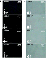
A uniform alignment state is important for high-quality LCD images. Fig. 1 shows a cross-polarised optical microscopy image of HfSnO-based LC cells as function of IB irradiation intensity. Uniform LC alignment was obtained, regardless of the IB irradiation intensity. This finding indicates that IB irradiation of the HfSnO films facilitated LC alignment. Moreover, when aligned, the homogeneous LC cells positioned between crossed polarisers determined light transmittance. When the LCs were aligned along one direction of the intersectional polariser, the transmittance was minimised, resulting in dark images (Fig. 1a). When the LC samples were rotated by 45° relative to the polariser, the transmittance was maximised and white images were observed (Fig. 1b). Therefore, the optical properties displayed in Fig. 1 indicate well-aligned, homogeneous LC alignment states on HfSnO films.
image file: c5ra09337f-f1.tif
Fig. 1 Photographs of liquid crystal (LC) cells, based on ion beam (IB)-irradiated HfSnO films prepared using various IB incident energies. “A” and “P” represent the analyser and polariser axes, respectively.

Transmittance measurements were performed under latitudinal rotation of LC samples using a crystal rotation method to calculate the pretilt angles of the LC molecules of IB-irradiated HfSnO films (Fig. 2). The blue (simulated) and red (experimental) curves in the insets of Fig. 2 are nearly identical, indicating that the LC alignment was stable; this allowed determination of the pretilt angles with high reliability. The calculated pretilt angles of each sample at 600, 1200, 1800, and 2400 eV were 0.18°, 0.09°, 0.06°, and 0.03°, respectively, with a low standard deviation (<0.01). A minimum of 10 points was measured on each cell of the samples. The low deviation of the pretilt angles indicated uniform LC alignment states over the entire area. The calculated data, including the pretilt angle and its deviations, and the transmittance oscillation graph obtained using the crystal rotation method, supported POM analysis results and numerically confirmed the uniformity and stability of the homogeneously aligned LC molecules on IB-irradiated HfSnO films.


image file: c5ra09337f-f2.tif
Fig. 2 The measured pretilt angles. (Insets) Transmittance measurement performed under latitudinal rotation using a crystal-rotation method on IB-irradiated HfSnO films prepared using various IB incident energies.

AFM was used to evaluate the topological effect of IB irradiation on the morphology of HfSnO films, before (Fig. 3a) and after (Fig. 3a) IB irradiation. IB irradiation reportedly modifies the morphology of pristine oxide films; IB induces a significant reduction in the film roughness,23 forming a uniform layer. Before IB irradiation, a bumpy, non-uniform surface was observed and grain agglomerations formed in HfSnO films. A root mean square (RMS) roughness of 13.545 nm was measured. Moreover, the sharpness degree of the surface height distribution, referred to as kurtosis, was 20.164. Kurtosis represents a Gaussian-like surface centred at 3. Uniformly formed grain was observed in irradiated films. The RMS roughness of the irradiated films was 2.037 nm and its kurtosis was 2.926 (<3). This value is similar to the roughness of rubbed PI which is typically 1 nm to 6 nm24,25. These results suggest that IB irradiation induces uniformity and reduces surface roughness. Moreover, the roughness change of IB-irradiated films could be one of the reasons for uniform LC alignment (Scheme 1).


image file: c5ra09337f-f3.tif
Fig. 3 AFM image of (a) before and (b) after IB irradiated HfSnO films.

image file: c5ra09337f-s1.tif
Scheme 1 Possible mechanism of LC alignment on HfSnO films before and after IB irradiation.

However, the aforementioned topological surface properties cannot explain the LC alignment mechanism completely, because IB irradiation induces not only physical modification, but also chemical modification of the irradiated surfaces.17 To determine the mechanism of LC alignment, we investigated the chemical modification of IB-irradiated HfSnO films using XPS.

Fig. 4 presents the XPS spectra of the Hf 4f, Sn 3d, and O 1s core levels for IB-treated and non-treated HfSnO films. Peaks were referenced to the neutral adventitious C 1s peak, defined at 285.0 eV. In the case of the HfO2 films, the Hf 4f peak was observed as a spin–orbit split doublet, with oxidised Hf 4f7/2 and Hf 4f5/2 peaks at 16.4 eV and 18.2 eV, respectively.26 However, the Hf 4f core levels appeared at higher binding-energy positions on HfSnO films both before and after IB irradiation. Hf 4f7/2 and Hf 4f5/2 peaks appeared at 17.3 eV and 19.1 eV, respectively, and subsequently no shift was observed between IB treatments. The shift compared with conventional Hf peaks may be related to the different structural phase and/or different bonding states between incorporated components.


image file: c5ra09337f-f4.tif
Fig. 4 (a) Hf 4f, (b) Sn 3d and (c) O 1s core-level XPS spectra of the surface according to the IB power intensity.

In the case of the SnO2, the binding energy of Sn 3d5/2 was centred near 486.2 eV, indicating the fully oxidised value of Sn27. Subsequently, only a slight negative shift of the Sn 3d peak was observed after IB irradiation. Theoretically, a negative shift represents lattice displacement of the film and surface damage.27 The O 1s peak shows a dominant peak shift after IB irradiation. Specifically, the oxygen peaks can be deconvoluted into two sub-peaks (O1 and O2), centred near 530.4 and 531.6 eV. The lower peak (O1) at 530.4 eV arises from oxygen in the oxide lattices, bonded with metal ions. The higher peak (O2) was assigned to the oxygen vacancy in the oxide films. The IB-irradiated HfSnO films showed a relatively higher fraction of oxygen vacancies (O2) than the non-treated HfSnO film, which is consistent with the results of lattice displacement and film damage from the aforementioned negative shifts in Sn 3d. Displacement and damage of the film may induce rearrangement of the structure. The higher fraction of oxygen vacancies indicates that IB irradiation breaks the oxygen bonds, which causes rearrangement of the structure and the creation of oxygen vacancies on the surface. The broken bonds and oxygen vacancies induce delocalised electron formation over the entire surface. The combination of these delocalised electrons and rearrangement of the structure may induce anisotropic dipole polarisation of the surface, thereby stabilising LC alignment along the direction of IB irradiation (Scheme 1).

Fig. 5 presents electro-optical characteristics, including the voltage–transmittance and response time of TN cells on IB-irradiated HfSnO films. TN cells, based on rubbed PI layers, were prepared for comparison. The TN cells were characterised by a ‘normally white’ mode, i.e., the homogeneously aligned TN-LC cells could be switched from ON to OFF when an external voltage was applied above a certain threshold (V > Vth at 90% transmittance). The threshold voltage, Vth, at 90% transmittance for TN cells on IB-irradiated HfSnO films with an IB intensity of 600, 1200, 1800, and 2400 eV were 1.879, 1.834, 1.828, and 1.827 V, respectively. Vth for IB-irradiated films was similar among the film samples, regardless of IB intensity (Table 1). Compared with conventional PI (Vth: 2.11 V), Vth at 2400 eV was reduced by 13.4%; thus, HfO, SnO, and HfSnO can be characterised as high-k dielectrics.


image file: c5ra09337f-f5.tif
Fig. 5 (a) Voltage–transmittance (VT) curve, (b) response time, and (c) anchoring energy characteristics of twisted nematic (TN) cells based on IB-irradiated HfSnO films.
Table 1 Summary of the electro-optical (EO) characteristics of twisted nematic (TN) cells with ion beam (IB)-irradiated HfSnO films prepared using various IB incident energies and rubbed polyimide (PI)
IB incident energy and rubbed PI Threshold voltage [Vth] Response time
Rise time (ms) Fall time (ms)
Rubbed PI 2.11 6.554 14.327
600 eV 1.879 7.22 11.313
1200 eV 1.834 7.433 11.064
1800 eV 1.828 7.263 9.656
2400 eV 1.827 6.688 8.119


The time–transmittance curves for IB-irradiated HfSnO and rubbed PI as a function of IB intensity show the rise and fall response times (Fig. 5b). IB-irradiated HfSnO films with an IB intensity of 2400 eV yielded the most rapid response time of 14.807 ms (rise and fall times of 6.688 and 8.119 ms, respectively) among the IB intensity conditions (Table 1). Conventional rubbed PI had a response time of 20.881 ms (rise and fall times of 6.554 and 14.327 ms, respectively). Compared with rubbed PI, LC cells based on IB-irradiated HfSnO films exhibited superior electro-optical performance. Moreover, the total response time of IB-irradiated thin films decreased as the IB intensity increased.

The decrease in the switching time (i.e., faster response time) with an increase in IB intensity may be related to the anchoring energy. XPS analysis revealed that stronger IB intensities broke the oxygen bonds, consequently inducing oxygen vacancy formation and the dispersion of delocalised electrons over the entire surface. Strong van der Waals interactions between the LC and IB-irradiated surface, caused by an increase in the number of delocalised electrons, may enhance the anchoring energy; the measured anchoring energy increased with the IB intensity (Fig. 5c and Table 2).

Table 2 Anchoring energy of TN cells with IB-irradiated HfSnO films prepared using various IB incident energies
IB incident energy [eV] 1200 eV 1800 eV 2400 eV
Anchoring energy [J m−2] 7.1245 × 10⁻⁵ 7.9945 × 10⁻⁵ 2.1733 × 10⁻⁴


The fall time of twisted nematic LCs is mainly affected by the anchoring energy of the LCs on the alignment layer.28 Moreover, the rise time of LCs is influenced by the operating conditions. In our system, the enhanced response time is strongly dependent on the fall response time with IB intensity, as opposed to the rise time. Consequently, the fast response time was attributed to the strongly reformed surface, specifically one with enhanced anchoring energy.

Image sticking is one of the most important issues affecting good quality displays. When the voltage is turned on, residual charges that accumulate at localised defect sites gradually dissipate over time, resulting in image sticking. The capacitance–voltage (CV) hysteresis of LC cells can measure the degree of image sticking caused by the capture of impurity charges, i.e., residual charges on the surface. Fig. 6 shows CV hysteresis curves of LC cells based on IB-irradiated HfSnO films as function of IB intensity. Unlike CV curves that exhibit characteristic hysteresis of LC cells prepared by low IB intensities, a nearly hysteresis-free CV curve was obtained for high-intensity IB-irradiated HfSnO films, as shown in Fig. 6c. This result is related to the physical and chemical modification of the surface as a function of the IB intensity. As the IB intensity increased, the strongly reformed surface effectively induced the release of volume charges upon switching of the LC molecules, which led to a surface nearly free of residual charges within the LC alignment layer interface (i.e., prevention of CV hysteresis).


image file: c5ra09337f-f6.tif
Fig. 6 Capacitance–voltage (CV) characteristics of LC cells based on IB-irradiated HfSnO films prepared using various IB incident energies.

Conclusions

In summary, we successfully demonstrated high-performance liquid crystal (LC) devices without capacitance hysteresis, using ion beam (IB)-irradiated HfSnO films as an alignment layer and controlling the IB intensity. AFM results demonstrated that IB irradiation of HfSnO reduced surface roughness and made the film surface more uniform. XPS analysis revealed that strong IB irradiation of solution-derived HfSnO films was responsible for the breaking of oxygen bonds at the film surface, which created oxygen vacancies and delocalised electrons over the entire surface. Strong van der Waals interactions between the LC and IB-irradiated surface with delocalised electrons enhanced the anchoring energy, which resulted in a more rapid response time compared with rubbed PI. Strongly reformed IB-irradiated HfSnO surfaces (i.e., high IB intensities) effectively induced the release of volume charges upon switching of the LC molecules, removing most of the residual charge within the LC alignment layer interface. Thus, IB-irradiated HfSnO films have great potential for use as an advanced LCD alignment layer free of CV hysteresis.

Notes and references

  1. T. Ikeda, J. Mater. Chem., 2003, 13, 2037 RSC.
  2. L. De Sio, A. E. Vasdekis, J. G. Cuennet, A. De Luca, A. Pane and D. Psaltis, Opt. Express, 2011, 19, 23532 CrossRef CAS PubMed.
  3. V. Caligiuri, L. De Sio, L. Petti, R. Capasso, M. Rippa, M. G. Maglione, N. Tabiryan and C. Umeton, Adv. Opt. Mater., 2014, 2, 950 CrossRef CAS.
  4. M. S. Li, A. Y.-G. Fuh, J.-H. Liu and S.-T. Wu, Opt. Express, 2012, 20, 25545 CrossRef CAS PubMed.
  5. M. F. Toney, T. P. Russell, J. A. Logan, H. Kikuchi, J. M. Sands and S. K. Kumar, Nature, 1995, 374, 709 CrossRef CAS.
  6. Y. J. Kim, Z. Zhuang and J. S. Patel, Appl. Phys. Lett., 2000, 77, 513 CrossRef CAS.
  7. J. V. Crivello, M. Deptolla and H. Ringsdorf, Liq. Cryst., 1988, 3, 235 CrossRef CAS.
  8. J. Y. L. Ho, V. G. Chigrinov and H. S. Kwok, Appl. Phys. Lett., 2007, 90, 243506 CrossRef.
  9. M. Liu, X. Zheng, S. Gong, L. Liu, Z. Sun, L. Shao and Y. Wang, RSC Adv., 2015, 5, 25348 RSC.
  10. P. Chaudhari, J. Lacey, J. Doyle, E. Galligan, S. C. A. Lien, A. Callegary, G. Hougham, N. D. Lang, P. S. Andry, R. John, K. H. Yang, M. Lu, C. Cai, J. Speidell, S. Purushothaman, J. Ritsko, M. Samant, J. Stöhr, Y. Nakagawa, Y. Katoh, Y. Saitoh, K. Sakai, H. Satoh, S. Odahara, H. Nakano, J. Nakagaki and Y. Shiota, Nature, 2001, 411, 56 CrossRef CAS PubMed.
  11. J. Y. Kim, B. Y. Oh, B. Y. Kim, Y. H. Kim, J. W. Han, J. M. Han and D.-S. Seo, Appl. Phys. Lett., 2008, 92, 043505 CrossRef.
  12. O. Yaroshchuk, R. Kravchuk, A. Dobrovolskyy, L. Qiu and O. D. Lavrentovich, Liq. Cryst., 2004, 31, 859 CrossRef CAS.
  13. C. Y. Lee, Y. L. Liu, K. Y. Wu, M. Y. Chen and J. C. Hwang, Jpn. J. Appl. Phys., 2008, 47, 226 CrossRef CAS.
  14. M. Schadt, H. Seiberle and A. Schuster, Nature, 1996, 381, 212 CrossRef CAS.
  15. K. Usami, K. Sakamoto and S. Ushioda, J. Appl. Phys., 2003, 93, 9523 CrossRef CAS.
  16. J. Stöhr, M. G. Samant, J. Lüning, A. C. Callegari, P. Chaudhari, J. P. Doyle, J. A. Lacey, S. A. Lien, S. Purushothaman and J. L. Speidell, Science, 2001, 292, 2299 CrossRef PubMed.
  17. H.-C. Jeong, H.-G. Park, J. H. Lee, Y.-H. Jung, S.-B. Jang and D.-S. Seo, Sci. Rep., 2015, 5, 8641 CrossRef CAS PubMed.
  18. B.-Y. Kim, Y.-H. Kim, H.-G. Park and D.-S. Seo, Liq. Cryst., 2010, 37, 1381 CrossRef CAS.
  19. H. G. Park, H. C. Jeong, J. J. Han, S. Y. Kim, J. H. Kim, D. H. Kim and D. S. Seo, J. Mater. Chem. C, 2014, 2, 3960 RSC.
  20. W. K. Lee, B. Y. Oh, J. H. Lim, H. G. Park, B. Y. Kim, H. J. Na and D. S. Seo, Appl. Phys. Lett., 2009, 94, 223507 CrossRef.
  21. D. C. Suh, Y. D. Cho, S. W. Kim, D. H. Ko, Y. Lee, M.-H. Cho and J. Oh, Appl. Phys. Lett., 2010, 96, 142112 CrossRef.
  22. P. Blake, P. Brimicombe, R. Nair, T. Booth, D. Jiang, F. Schedin, L. Ponomarenko, S. Morozov, H. Gleeson, E. Hill, A. Geim and K. Novoselv, Nano Lett., 2008, 8, 1704 CrossRef PubMed.
  23. K.-W. Lin, M. Mirza, C. Shueh, H.-R. Huang, H.-F. Hsu and J. van Lierop, Appl. Phys. Lett., 2012, 100, 122409 CrossRef.
  24. S.-J. Kang, Y.-Y. Noh, K.-J. Baeg, J. Ghim, J.-H. Park and D.-Y. Kim, Appl. Phys. Lett., 2008, 92, 052107 CrossRef.
  25. W. Zheng, C.-H. Lu and Y.-C. Ye, Jpn. J. Appl. Phys., 2008, 47, 1651 CrossRef CAS.
  26. D. D. Sharma and C. N. R. Rao, J. Electron Spectrosc. Relat. Phenom., 1980, 20, 25 CrossRef.
  27. Y. Gotoh and O. Okada, J. Nucl. Sci. Technol., 1984, 21, 205 CrossRef CAS.
  28. M. Jiao, Z. Ge, Q. Song and S.-T. Wu, Appl. Phys. Lett., 2008, 92, 061102 CrossRef.

This journal is © The Royal Society of Chemistry 2015
Click here to see how this site uses Cookies. View our privacy policy here.