DOI:
10.1039/C5RA09188H
(Review Article)
RSC Adv., 2015,
5, 78109-78127
Fabrication of paper-based microfluidic analysis devices: a review
Received
17th May 2015
, Accepted 4th September 2015
First published on 7th September 2015
Abstract
When compared with conventional microfluidic chips made of glass and polymer substrates, paper-based microfluidic analysis devices (μPADs) possess many unique advantages, including low-cost, easy-to-fabricate, strong capillary action and good biological compatibility. In recent years, μPADs have attracted increased interest and attention, which has led to their rapid development. Thousands of literature reports regarding μPADs have been published and a variety of μPADs fabrication methods have been reported. This review focuses on the development of the fabrication methods of 2D and 3D μPADs since 2007. A summary of the advantages and disadvantages of these methods is provided with particular attention paid to the resolution and cost of each method. Suitable applications of each method are discussed. Also, some trends of μPADs are summarized.
 Yong He | Yong He obtained his B.E. in engineering mechanics at the China University of Mining and Technology in 2001. He obtained his Ph.D. degree in mechanical engineering at the Zhejiang University in 2008. He is currently an associate professor at Zhejiang University, College of Mechanical Engineering. Also he is the deputy director of Key Lab of 3D Printing Process and Equipment of Zhejiang Province. His research is focused on the cell printing, development of organ on a chip and microfluidic analytical device. Now he has published over 30 papers and authorized over 20 patents. |
 Yan Wu | Yan Wu received her B.E. in Mechanical Engineering from Zhejiang University in 2014. She is currently a graduate student in the College of Mechanical Engineering at Zhejiang University. Her research focuses on the development of paper-based microfluidic analytical devices. |
 Jian-Zhong Fu | Jiang-zhong Fu obtained his B.E., M.S. and Ph.D. in mechanical engineering at Zhejiang University, in July 1990, 1992 and 1996, respectively. He is currently a professor at Zhejiang University, College of Mechanical Engineering. He is a vice dean of the College of Mechanical Engineering. His research is focused on 3D printing, numerical control, and micro fabrication. Now he has published over 50 papers and authorized over 20 patents. |
 Wen-Bin Wu | Wenbin Wu received his B.E. in Mechanical Engineering from Zhejiang University in 2013. He is currently a graduate student in the College of Mechanical Engineering at Zhejiang University. His research focuses on the development of low-cost microfluidic analytical devices with 3D printing technology. |
1. Introduction
Paper-based microfluidic devices have enjoyed rapid development since Whitesides et al.1 introduced the μPADs concept. A series of hydrophilic/hydrophobic microstructures on paper substrates were fabricated to construct μPADs using a variety of processing techniques. Compared to conventional microfluidic chips made of glass and polymer substrates, μPADs possess many unique advantages including, low-cost, ease of fabrication, strong capillary action and good biological compatibility for applications in clinical diagnosis, food quality control and environmental monitoring. The overlying purpose of fabricating μPADs is to provide a low-cost, environmentally friendly analytical chemistry tool that is suitable for field testing and point-of-care (POC) diagnosis. Recently, a number of scholars have proposed a variety of methods for fabricating μPADs, including wax printing,2–6 plotting,7,8 inkjet etching,9,10 flexographic printing,11 laser treatment,12–15 ink stamping,16–18 paper cutting and shaping,19–24 lacquer spraying,25 screen-printing,26,27 photolithography,28–34 plasma treatment,35–37 inkjet printing,38–40 chemical vapor-phase deposition,41–44 wet etching,45 hand-held corona treatment,46 among others. Some methods are physical processes, such as, ink stamping and plotting; some are chemical processes, like plasma treatment and photolithography; some are environmentally friendly processes, such as wax printing; while some require the use of toxic substances during the processes, like photolithography. A variety of methods are suitable for field testing, such as, ink stamping, and some are suitable for mass production, like inkjet printing. Each method is expedient for certain applications, although individual limitations exist. This review focuses on the development of the fabrication methods of μPADs since 2007. In this, we analyze the resolution and cost of the fabrication methods and try to categorize the applications of the various methods. More importantly, according to the features of each method, recommended applications are discussed.
2. Fabrication methods
There are many different categories of fabrication methods of μPADs such as wax patterning, inkjet printing, photolithography, plotting and laser treatment. In this chapter, we divide the fabrication methods of μPADs into two categories based on their physics and chemistry.
2.1 Physical methods
2.1.1 Wax patterning. Wax is a cheap hydrophobic material, which has been widely used in the fabrication of μPADs, since it can be applied to paper by a variety of methods.In 2009, Lin et al.2 and Whitesides et al.3 reported a new method, wax printing, to fabricate μPADs. A solid wax printer was used to print wax on filter paper in a designed pattern.2 The printed wax was then melted in an oven. Due to the porous structure of the filter paper, the wax penetrates into the paper to form well-defined micro-channels on the paper. The whole process is simple and requires only a wax printer and an oven. But the resolution of the μPADs fabricated by this method is limited to millimeters (Fig. 1a). Whitesides et al.3 reported a similar method and established a model for the melt rate of wax in the filter paper (Fig. 1b). In 2012, a fully enclosed μPADs fabricated by printing wax and toner was introduced.4 Wax was printed as hydrophobic barriers, while the toner was printed on the top and bottom of the paper as a seal. In this way, the analytical reagent can be protected from contamination (Fig. 1c). As wax printing is easy to be implemented by a wax printer, now it has already become a major μPADs fabrication method. But there is a minor problem about the wax printer, which makes it fail in competition with laser printer and inkjet printer. Probably, in the next few years, it is different to purchase a wax printer.
 |
| Fig. 1 The process of (a) Wax printing. Reprinted from ref. 2. Copyright 2009, with permission from WILEY-VCH Verlag GmbH & Co. KGaA, Weinheim. (b) Wax printing. Reprinted from ref. 3. Copyright 2009, with permission from American Chemical Society. (c) Wax and toner printing. Reprinted from ref. 4. Copyright 2012, with permission from American Chemical Society. (d) Wax dipping. Reprinted from ref. 5. Copyright 2015, with permission from Elsevier. | |
Wax dipping was used to fabricate μPADs as described by Songjaroen et al.5 In this process, an reusable iron mold was fabricated using by a precise laser cutting technique. In the next step, filter paper was placed onto a glass slide and then the mold was placed onto the paper and it was temporarily attached by means of magnetic force using a permanent magnet placed on the backside of the glass slide. Next, the assembly was dipped for one second into a chamber of melted wax that was maintained at a temperature of 120–130 °C. After the paper was cooled to room temperature, it was peeled off of the glass slide and the iron mold was removed from the paper. Finally, the hydrophobic and hydrophilic areas of the μPADs were produced (Fig. 1d).
Zhang et al.6 reported another wax dipping method to fabricate μPADs using printed circuit technology. Patterns of channels were initially designed and printed and then transferred to a copper sheet using a thermal transfer printer. Then, the sheet copper was dipped into ferric chloride solution to etch the patterns. Next, the etched sheet copper was coated with a film of paraffin and then a piece of filter paper. Finally, a common, consumer electric iron was used to heat the back side of the sheet copper and the melted paraffin penetrated the full thickness of the filter paper and formed a hydrophobic wall. In wax dipping, preparation of the mask mold is a time-consuming process which limits its flexibility.
2.1.2 Plotting. Whitesides and coworkers7 used a modified x–y-plotter to fabricate μPADs. They printed a solution of a hydrophobic polymer (polydimethylsiloxane, PDMS) dissolved in hexane onto a filter paper using a modified x–y-plotter. The PDMS penetrated the depth of the paper and formed a hydrophobic wall that prevented access to aqueous solutions. This method is low-cost and the resulting μPADs are physically flexibility. A wax pen was also used as a simpler method to fabricate μPADs.2 First, the desired patterns were traced in wax on the both sides of a piece filter paper. Then the treated filter paper was placed in the oven at a temperature of 150 °C for about 5 min. The wax patterns melted and penetrated the paper to form a hydrophobic wall on the paper. A similar method was reported by Li and workers8 to fabricate μPADs by (Fig. 2a). The difference between these two methods was that Li used commercially available permanent markers in place of a wax pen. In this manner, the μPADs could be fabricated in a single step, without heating. Although plotting is low-cost and simple, it is hard to control the size of hydrophobic barrier; thus, complex patterns cannot be fabricated by this kind of method, which seriously limits its use.
 |
| Fig. 2 The process of (a) Plotting. Reprinted from ref. 8. Copyright 2012, with permission from American Chemical Society. (b) Inkjet printing. Reprinted from ref. 9. Copyright 2008, with permission from American Chemical Society. (c) Flexographic printing. Reprinted from ref. 11. Copyright 2010, with permission from American Chemical Society. (d) Laser treatment. Reproduced from ref. 14 with permission from the Royal Society of Chemistry. | |
2.1.3 Inkjet etching. Generally speaking, etching is a kind of manufacturing process of semiconductor. With the development of micro-manufacture process, the etching becomes a common name which by means of using a solution, a reactive ion or other mechanical means to peel or remove the material. Abe et al.9,10 used an inkjet etching technique to fabricate μPADs (Fig. 2b). The process begins with soaking a piece of filter paper in a 1.8 wt% solution of polystyrene dissolved in toluene for 2 hours. The treated filter paper was then removed from the solution where it becomes hydrophobic after the solvent evaporates. Next, an inkjet printer is used to pattern toluene on the test lines, control lines and channels in 10–20 repeated moves to remove the polystyrene deposited in these areas. This forms the hydrophobic barriers and hydrophilic channels. In this method, the process that polystyrene is peeled from the filter paper by toluene is seen as etching. The toluene is the etchant and the filter paper with polystyrene is etched. Although μPADs made by this method have high resolution, the fabrication process is rather complex.
2.1.4 Flexographic printing. The flexographic printing technique is a type of direct printing that can be used to fabricate μPADs11 (Fig. 2c). Polystyrene is printed on the filter paper using the flexographic printing technique. The polystyrene penetrates into the depth of the filter paper and forms a hydrophobic wall. The regions of the filter paper that do not contain polystyrene are hydrophilic. This method may not be suitable to be used in the lab for the prototype fabrication, however, it can be used for mass production of μPADs and has a promising future.
2.1.5 Laser treatment. Laser treatment has been widely used in the fabrication of μPADs and a number of researchers have used different kinds of laser treatment method to fabricate μPADs. This method requires the use of expensive equipment and careful processing, which limits its use.Ziaie et al.12 reported a laser treatment μPAD fabrication method that entailed the use of parchment paper as the substrate. The parchment paper was spread open, placed on a platform and surface treated using a computer-controlled CO2 laser cutting and engraving system. The desired pattern was printed onto the parchment paper by raster-scanning the laser beam across the surface. In this process, the laser power and scanning speed were carefully selected to avoid cutting through the paper. After the initial treatment, the patterned areas were coated with silica micro particles to enhance directional wettability of the surface. Wax paper and palette paper can also be used in this method.
A CO2 laser cutting and ablative etching method was reported for the fabrication of μPADs.13 This entailed first sandwiching a nitrocellulose substrate between two thin polymer layers. The CO2 laser was then used to selectively remove material to define the channel walls. Finally, the protective layers were removed and the paper networks were ready for use. More recently, a similar method was also reported using a CO2 laser cutting/engraving machine to fabricate μPADs14 (Fig. 2d).
2.1.6 Ink stamping. The general process of stamping is prevalent in common life. Its ease and convenience have prompted of use many researchers to try and fabricate μPADs using different types of stamps and ink.In this regard, a stamp and indelible ink have been used to fabricate μPADs.15 Researchers have defined a microfluidic structure by contact stamping of indelible ink on filter paper using a PDMS stamp. The workers pushed the PDMS stamp three times into the indelible ink saturated stone pad and placed the PDMS stamp in contact with the filter paper for 3 s, without the application of force. This resulted in the desired μPAD. This method is low-cost and simple, but the fabrication of the PDMS stamp appears to be quite complex.
A handheld stamp was used as the tool to pattern the filter paper16 prior to fabrication of the μPAD (Fig. 3a). First, a piece of filter paper was immersed in liquid paraffin and solidified at room temperature and then it was placed on the native paper surface. A metal stamp was preheated and brought in contact with the paraffined paper to stamp the microfluidic structure on the n-paper, which transferred the paraffin from the p-paper to the n-paper and formed the hydrophobic barriers.
 |
| Fig. 3 The process of (a) Handheld stamping. Reproduced from ref. 16 with permission from the Royal Society of Chemistry. (b) FFSL. (c) Paper cutting. Reprinted from ref. 18. Copyright 2009, with permission from American Chemical Society. (d) LPAD. Reprinted with permission from ref. 19. Copyright 2013, with permission from Spring-Verlag Berlin Heidelberg. (e) Open channels. Reprinted from ref. 20. Copyright 2014, with permission from American Chemical Society. | |
For the stamping method, rapid fabrication of stamp and easy stamping are both very important. Therefore, our group introduced the flash foam stamp to fabricate μPADs, which is named as flash foam stamp lithography (FFSL) (Fig. 3b). This consisted of, initially forming a flash foam stamp with the desired patterns using flash exposure. Next, the stamp was immersed in polydimethylsiloxane (PDMS) to absorb the ink. Finally, the PDMS was stamped on a piece of filter paper to form hydrophobic barriers and the μPADs were finished. As the flash foam stamp is widely used as a personal stamp, the fabrication of a flash foam stamp is very easy. Another advantage of this stamp is that the ink can be stored inside, which is convenient to transfer patterns to the paper. We verified this method as a cheap and quick approach. However, this method is more suitable for rapid prototype design in the lab.
2.1.7 Paper cutting and shaping. Fenton et al.18 fabricated paper and nitrocellulose-based lateral-flow devices using a computer-controlled knife (Fig. 3c). These authors used a computer-controlled x–y knife plotter, which incorporated a knife in place of the traditional ink pen. To cut the paper without tearing it, they used three sequential overlapping cuts. The whole process requires only 60 s to complete and this method is low-cost and well suited in many cases.In a similar method, paper cutting and shaping was used to fabricate laminated paper-based analytical devices (LPADs)19 (Fig. 3d). In this instance, the authors used a simple craft cutter to cut a section of chromatography paper, which was affixed to an adhesive carrier sheet. After cutting, the cover, paper strip and bottom sheet were aligned and assembled together. In addition, the cover sheet also need being open for sample accesses by the craft cutter.
More recently, an easy approach for fabricating μPADs has been presented that employs programmed fluid transport within a paper-based device to enable both acceleration and delay of fluid transport without active pumping20 (Fig. 3e). These authors carved open channels either longitudinally or perpendicularly to the flow path by a craft-cutting tool equipped with a knife blade. In this way, accelerated and reduced fluid transport rates were achieved using the same device.
Glavan et al.21 cut carved channels in omniphobic paper (Fig. 4a). The combination of omniphobic paper and a craft cutter produced new valves and switches, such as “fold valves” and “porous switches”, which provided new methods to control fluid flow. A μPAD that relied on flow in hollow channels to transport fluids was reported.22 Patterns were printed on paper using a wax printer. The paper was then placed in an oven at 120 °C for 1 min and then cooled to 20 °C. Finally, the paper channels and reservoirs were cut using, respectively, a razor blade and a 4 mm inner-diameter punch. The flow rate in the hollow channels was 7 times higher than in regular paper channels and it could be conveniently controlled from zero to several mm s−1 by balancing the capillary and pressure forces.
 |
| Fig. 4 The process of (a) omniphobic paper cutting. Reproduced from ref. 21 with permission from the Royal Society of Chemistry. (b) Embossing. Reprinted from ref. 23. Copyright 2014, with permission from American Chemical Society. (c) Lacquer spraying. Reprinted with permission from ref. 24. Copyright 2015, with permission from Elsevier. (d) Wax screen-printing. Reproduced from ref. 25 with permission from the Royal Society of Chemistry. (e) Polystyrene screen-printing. Reproduced from ref. 26 with permission from the Royal Society of Chemistry. | |
A new method of using embossing and a cut-and-stack method of assembly to generate microfluidic devices from omniphobic paper has been described23 (Fig. 4b). In this process, a sheet of paper was placed between two plastic molds, which had been previously processed by a punch and concave dye, and pressed for dimensions. Before embossing the paper, a few drops of ethanol was placed on the paper to wet its surface to increase its molding ability. Once embossing was finished, the paper was allowed to dry for 30 s in an oven at 60 °C, then the μPAD was finished. With this method, a three-dimensional micro channels can be fabricated on the paper.
All paper cut-based method may have a drawback-difficult to precisely control the channel size. And another limitation is that the assembly process may be only suitable for handle operation and fabricating prototype μPADs.
2.1.8 Lacquer spraying. A spraying method using lacquer was developed by Nurak et al. for the fabrication of μPADs24 (Fig. 4c). This entailed sandwiching a filter paper between a patterned iron mask and a magnetic plate. Following this, an acrylic lacquer was sprayed on the filter paper to create a hydrophobic area while the hydrophilic area was protected by the iron mask. This method is simple and low cost, however, the iron mask may be troublesome.
2.1.9 Screen printing. Wax screen-printing was also used to fabricate μPADs25 (Fig. 4d). Here the model of screen-printing is first fabricated and then solid wax is rubbed through the screen model onto the filter paper. The printed wax was then heated and melted into the paper to form hydrophobic barriers using a hot plate. The same method was also reported by Sameenoi et al.26 to fabricate μPADs. However, in this instance, they authors replaced the wax with polystyrene (Fig. 4e). As screen printing is very common in fabricating bits of printing materials, this method is suitable for small amounts μPADs fabrication.
2.2 Chemical methods
2.2.1 Photolithography. Whitesides et al.1 have reported the fabrication of μPADs using photolithography. The authors patterned chromatography paper using SU-8 2010 photoresist (Fig. 5a) and then soaked and spun the photoresist on chromatography paper, which was and baked at 95 °C for 5 min to remove the cyclopentanone in the SU-8 formula. The paper was then exposed to 405 nm UV light for 10 s through a photo mask that was aligned using a mask aligner. After exposure, the paper was baked a second time at 95 °C for 5 min to cross-link the exposed portions of the resist. The unpolymerized photoresist was removed by soaking the paper in propylene glycol monomethyl ether acetate and then washing the pattern. Finally, the paper was exposed to an oxygen plasma to increase the hydrophilicity of the paper. The fabricated μPADs enjoy high resolution, but SU-8 is expensive and the process is complex. Later, to reduce the cost, Whitesides and co-workers used an epoxy negative photoresist27 and an SC photoresist28 (Fig. 5b) in place of SU-8 2010 photoresist.
 |
| Fig. 5 The process of photolithography (a) SU-8 2010 photoresist. Reprinted with permission from ref. 1. Copyright 2007, with permission from WILEY-VCH Verlag GmbH & Co. KGaA, Weinheim. (b) SC photoresist. Reprinted from ref. 28. Copyright 2009, with permission from American Chemical Society. (c) FLASH. Reproduced from ref. 27 with permission from the Royal Society of Chemistry. (d) OTS. Reprinted from ref. 29. Copyright 2013, with permission from American Chemical Society. (e) Ultraviolet resin. Reproduced by permission of The Royal Society of Chemistry. (f) Laser-based direct-write technique. Reprinted from ref. 32. Copyright 2014, with permission from American Chemical Society. (g) TiO. Reprinted with permission from ref. 34. Rights managed by AIP Publishing LLC. | |
Although high resolution can be acquired with photolithography, the expensive cost limits its wide use. So a lot of methods based on photolithography are proposed to reduce the cost and increase its flexibility. To avoid the use of lithography machine, a common UV lamp and a hotplate was used to solidify photoresist by Whitesides and co-workers.27 Also octadecyltrichlorosilane and deep UV-lithography were reported to fabricate μPADs.29 Since the fabrication of photomask will cause a long waiting time and increase the cost, a LCD or a digital micromirror device was used to generate the dynamic photomask immediately by our group.30 With this method, a μPAD can be fabricated within around 2 min including the design period. Also photomaskless methods were reported such as laser direct writing.34 However, as the XY stage needs to move in the maskless methods, the fabricating speed may be slow.
This formed the basis for a new method called FLASH (fast lithographic activation of sheets), which was reported for the fabrication of μPADs27 (Fig. 5c). FLASH is based on photolithography, but requires only a UV lamp and a hotplate. The process entails pouring the photoresist onto the paper and spreading the photoresist evenly around the paper. The paper was then baked on a hotplate and allowed to cool to room temperature. Next, the paper was sandwiched between an adhesive transparency film and a black paper. After exposing the paper to UV light, the paper was heated on a hotplate. Finally, the paper was soaked in acetone and rinsed with acetone and 70% isopropyl rubbing alcohol and dried under ambient conditions.
He et al.29 described the fabrication of μPADs by means of a coupling of hydrophobic silane to paper fibers followed by deep UV-lithography (Fig. 5d). Here, the filter paper is first immersed in an octadecyltrichlorosilane (OTS) solution dissolved in n-hexane. The filter paper becomes hydrophobic, because the OTS molecules are coupled to paper's cellulose fibers. The hydrophobized paper is then exposed to deep UV light through a patterned quartz mask. The UV-exposed regions become highly hydrophilic and form hydrophobic walls, whereas the masked regions remained highly hydrophobic.
A desktop stereolithography 3D printer was used to fabricate μPADs (Fig. 5e) in our group, which was called dynamic mask photo curing (DMPC).30 In this process, we first immersed the filter paper in ultraviolet resin to evenly cover it. Then the filter paper was exposed to UV-light through a dynamic mask with a negative channel pattern. After curing, the UV-exposed regions became highly hydrophobic and hydrophobic barriers were formed. Finally, the paper was washed to remove the uncured resin with anhydrous alcohol. This method requires only 2 minutes to fabricate a μPAD, despite the complexity of the patterns. In addition, this method is also low-cost and easy.
A simplified photolithography and cutting method has been described by Liang and coworkers.31 This entails, first, SU-8 2150 negative photoresist was thinned with trichloromethane and was coated onto the filter paper by hand. Then, the photo mask was placed on the coated paper and exposed to UV light. After the exposure, the unpolymerized photoresist was removed by washing the paper in acetone. This simplified photolithography method saves the amount of SU-8 and fabrication time for patterning μPADs.
More recently, a similar method using a laser-based direct-write technique was demonstrated by He and his group32 (Fig. 5f). Here nitrocellulose was used as the substrate and the fluidic patterns were created using a laser-based direct-write technique. Using this method, the group has successfully achieved a barrier-wall size that has yet to be achieved employing other reported methods.
A laser-based direct-write approach was also used to create patterns in paper.33 The paper substrate was initially soaked in the light-sensitive polymer and dried at ambient conditions. The authors used the principle of light-induced photo-polymerisation to pattern the paper. Compared to other laser treatment methods, this method is maskless.
Songok et al.34 reported a two-step fabrication process to fabricate μPADs using UV light and TiO2 (Fig. 5g). They used a high-speed, roll-to-roll liquid flame spray technique to coat TiO2 nanoparticle on the paper to form a hydrophobic surface. The hydrophilic pattern was then generated by UV irradiation through a photomask based on the photocatalytic property of TiO2.
2.2.2 Plasma treatment. Plasma treatment was commonly used in the assist of microfludic chip bonding. It was reported to make microfluidic patterns on paper surface by Li et al.35 The filter paper was dipped in an AKD–heptane solution and then removed and placed in a fume hood to allow evaporation of the heptane. The filter paper was then heated in an oven to cure the AKD, to render the paper hydrophobic. The filter paper was sandwiched between two metal masks with the desired patterns and then placed into a vacuum plasma reactor for 15 s. The exposed areas became hydrophilic following the plasma treatment. AKD, as a common industrial material, is cheap and readily available. Metal masks, however, are peculiar to each pattern. Therefore, the metal masks should be expensive and troublesome.Kao et al.36 demonstrated to use fluorocarbon plasma polymerization for fabrication of μPADs (Fig. 6a). The filter paper was tightly sandwiched between two masks, a positive mask and negative mask. The sandwich is then placed in a plasma system so that the fluorocarbon can penetrate through the paper to build hydrophobic barriers. This method is rapid and simple.
 |
| Fig. 6 The process of (a) Fluorocarbon plasma treatment. Reprinted with permission from ref. 36. Copyright 2014, with permission from Springer-Verlag Berlin Heidelberg. (b) Inkjet printing. Reproduced from ref. 40 with permission from the Royal Society of Chemistry. (c) Vapor phase deposition. Reproduced from ref. 42 with permission from the Royal Society of Chemistry. (d) Vapor phase deposition. Reproduced from ref. 43 with permission from the Royal Society of Chemistry. (e) Vapor phase deposition. Reprinted from ref. 44. Copyright 2013, with permission from American Chemical Society. (f) Wet etching. Reprinted with permission from ref. 45. Rights managed by AIP Publishing LLC. | |
Poly(hydroxybutyrate) and plasma have been reported for the fabrication of μPADs by Obeso and coworkers.37 The plasma process is similar to the plasma treatment described previously. However, in this case, the paper is successively immersed in different solutions and dried at room temperature before the plasma treatment. In this method, the plasma process is simple, but the production of the paper before plasma treatment is time consuming.
2.2.3 Inkjet printing. The previously described plasma treatment method has been improved by Shen et al. and now is used to fabricate μPADs with inkjet printing.38 The filter paper is printed using a reconstructed commercial digital inkjet printer employing an AKD–heptane solution. Then the printed paper is heated in an oven at 100 °C for 8 min to cure AKD onto the cellulose fibres. After the paper is dry, the μPAD is complete. Compared to the plasma treatment method, the inkjet printing method is maskless, simple and cheap. Wang et al.39 compared methylsilsesquioxane (MSQ) to wax and AKD as hydrophobic barrier material in the fabrication of μPADs using inkjet printing. The authors found that only the MSQ barriers were not breached by aggressive cell lysing solutions and surfactant solutions, which proved that MSQ is more suitable for fabricating μPADs.A similar method of inkjet printing was also used by Maejima et al. to fabricate μPADs.40 However, in this instance, they used a hydrophobic UV curable acrylate composition composed of non-volatile and nonflammable compounds to replace AKD (Fig. 6b). After printing the special ink on the paper, the paper was cured under UV light for 60 s and then hydrophobic barriers were formed. This method is low-cost and simple.
With inkjet printing, different types of reagents can be deposited on the paper at one time, it is promising in μPADs mass fabrication. However, the modified inks to carry reagents should be carefully designed to avoid blocking the nozzle. As a result, more researches are needed to work on how to design suitable inks before it becomes a mass fabrication method.
2.2.4 Chemical vapor-phase deposition. Fabrication of μPADs using chemical vapor-phase deposition of functional polymers was reported for the first time by Gupta et al.41,42 (Fig. 6c). Then, a similar method was reported for fabricating μPADs using vapor-phase deposition of pure polymers43 (Fig. 6d). In this latter process, the filter paper was sandwiched between a metal mask and a magnet. An appropriate amount of monomer was placed into an evacuated sublimation chamber and the monomers were then evaporated and converted to radical monomers by pyrolysis. These were subsequently deposited and polymerized onto the exposed region of the paper to form hydrophobic barriers. Gupta et al.44 also used this method to fabricate μPADs (Fig. 6e). The only difference between the two methods is that Gupta et al. used a different polymer, fluoropolymer coating of poly(1H,2H,2H-perfluorodecyl acrylate).
2.2.5 Wet etching. Cai et al.45 developed a fabrication method for μPADs using selective wet etching of hydrophobic filter paper employing a paper mask with a specific pattern (Fig. 6f). This entailed, first patterning filter paper using a trimethoxyoctadecylsilane (TMOS) solution. Next, a paper mask penetrated with NaOH solution was aligned onto the patterned paper, which allowed etching of the silanized paper by the etching reagent. The masked region became hydrophilic whereas the unmasked region remained hydrophobic.
2.2.6 Hand-held corona treatment. A hand-held corona treater was used by Jiang and coworkers to fabricate μPADs.46 First, a filter paper was coupled with octadecyltrichlorosilane (OTS) to render the paper hydrophobic. Then, the hydrophobic paper was exposed to the corona with a plastic mask. As a result, the exposed region became hydrophilic whereas the unexposed region remained hydrophobic.
3. Fabrication methods of 3D μPADs
To realize a multistep orderly chemical reaction or multiple preprocessing steps solely on one chip and improve the speed and efficiency of the analysis process, workers have investigated fabrication methods of 3D μPADs based on 2D μPADs. Recently, two methods for 3D μPADs fabrication have been reported; stacking and origami.
Three dimensional μPADs have stereo channels, which makes 3D μPADs superior to 2D μPADs. Compared to 2D μPADs, 3D μPADs offer the advantage of higher flow speed, because the length in the z direction is shorter than in the x–y plane. In addition, a 3D μPAD can contain a variety of simultaneous experiments. Finally, each layer of 3D μPADs can be used to realize different functions. For example, the first layer can be used as a filtration layer.
In addition, 3D μPADs are based on 2D μPADs, so the fabricating methods here simply refer to how 2D μPADs can be transformed into 3D μPADs.
3.1 Stacking
Whitesides et al.47,48 described a method for fabricating 3D μPADs by stacking layers of patterned paper and double-sided adhesive tape (Fig. 7a and b). Double-sided adhesive tape was punched with holes and the holes were filled with cellulose powder. The two pieces of the patterned filter paper were separated by the punched double-sided tape and the holes with cellulose powder linked these two pieces of paper. Later, their group used the same method without the cellulose powder in the holes49 (Fig. 7c). In this way, 3D μPADs were fabricated with single-use “on” buttons. However, it was found that it was difficult to align the paper and tape.
 |
| Fig. 7 The stacking process of 3D μPADs fabrication. (a) Double-sided tape. Reprinted with permission from ref. 47. Copyright (2008), with permission from National Academy of Sciences, U. S. A. (b) Double-sided adhesive tape. Reproduced from ref. 48 with permission from the Royal Society of Chemistry. (c) Tape for “on” buttons. Reproduced from ref. 49 with permission from the Royal Society of Chemistry. | |
In 2012, a method of wax printing and adhesive spraying was used to batch fabricate 3D μPADs50 (Fig. 8a). First, the authors patterned 2D μPADs using a wax printer. Next, they sprayed adhesive on one side of the paper and aligned the next layer and pressed it with a roller. The second step was repeated to add more layers until the 3D μPADs was completed.
 |
| Fig. 8 The stacking process of 3D μPADs fabrication. (a) Adhesive spraying. Reproduced from ref. 50 with permission from the Royal Society of Chemistry. (b) Bookbinding. Reprinted ref. 51. Copyright 2015, with permission from WILEY-VCH Verlag GmbH & Co. KGaA, Weinheim. | |
Xiao and his partners51 reported a method to fabricate 3D μPADs using staples (Fig. 8b). They first patterned each layer of the 3D μPADs using wax printing. Then they aligned and stacked the patterned papers and bound them using staples to ensure a close contact of adjacent layers. This method is rapid and suitable for mass fabrication.
3.2 Origami
Liu et al.52 reported the fabrication of 3D μPADs using origami (paper folding) (Fig. 9a). They first patterned each layer of μPADs on one filter paper by photolithography. Then they folded the paper following the fold. Finally an aluminum clamp was used to clamp layers and the 3D μPAD was complete. This method is simple except for the aluminum clamp. In a similar method, other researchers also fabricated 3D μPADs by origami53 (Fig. 9b). In this case, they replaced the aluminum clamp with a folder. Koo et al.54 made a paper-based microfluidic batteries using origami (Fig. 9c).
 |
| Fig. 9 The origami method of 3D μPADs fabrication. (a) Reprinted from ref. 52. Copyright 2011, with permission from American Chemical Society. (b) Reproduced from ref. 53 with permission from the Royal Society of Chemistry. (c) Reprinted with permission from ref. 54. Rights managed by AIP Publishing LLC. | |
4. Discussion
The goal of producing μPADs is to provide a low-cost, flexible analytical tools. Based on this intention, the methods for fabrication of μPADs are intended to be low-cost, convenient and rapid. In addition, it is more convenient to fabricate μPADs on site for rapid analysis. In this section, we compare each fabrication method and discuss possible applications. Some developments in the future are addressed including flow control of μPADs and μPAD-based instruments.
4.1 Comparison
Resolution and cost are two of the most important evaluation standards to evaluate the fabrication method of μPADs. Here, we define the amount of money needed to fabricate a μPAD as cost. It includes the cost of materials like filter paper and reagent, the cost of equipment used in the fabrication process and so on. The best fabrication method should be low-cost and offer high resolution. A variety of fabrication methods have been discussed and now the resolution and cost of these methods will be evaluated. Table 1 shows the resolution and cost of each method. What's more, we also point out the material and reagent used in each method, and compare the advantages and disadvantages of each method. We hope readers can understand the information of each fabrication method clearly from Table 1. It should be noticed that different resolution is required in different applications. In general, we can recognize two objects at the distance of larger than 0.1 mm with eyes from the distance of 30 mm. Thus, we recommend that the μPAD size resolution of 0.2 mm is enough in consideration of better recognition in the colorimetric detection.
Table 1 Resolution and cost of each method
Method |
Material and reagents |
Resolution (μm) |
Cost |
Advantages |
Disadvantages |
Barrier |
Channel |
Wax printing |
Wax |
850 ± 50 |
561 ± 45 |
Low |
Simple and fast to fabricate, mass production |
Low resolution, not resistant to high temperature |
Wax dipping |
Wax |
— |
639 ± 7 |
Low |
Simple and fast to fabricate, mass production |
Low resolution, need to be heated |
Printed circuit technique |
Paraffin |
— |
2000 |
Low |
Low cost, easy to fabricate |
Low resolution, not resistant to high temperature |
Plotting |
PDMS |
∼1000 |
∼1000 |
Low |
Cheap reagent, keep the filter paper flexible |
Low resolution, can't mass product |
Wax or marker |
— |
— |
Low |
Cheap reagent, simple steps, easy to fabricate |
Can't make complex feature, can't mass product |
Inkjet etching |
Polystyrene |
— |
— |
Low |
Low cost, biochemical reagents can be directly printed |
Complex steps, hydrophilic channels need to be printed many times |
Flexographic |
Polystyrene |
— |
— |
High |
Mass production |
Complex reagents and templates |
Laser treatment |
— |
62 ± 1 |
62 ± 1 |
High |
High resolution |
Expensive, need to overwrite nanoparticles |
Laser-based direct-write |
Light-sensitive polymer |
∼120 |
∼80 |
High |
High resolution, complex pattern |
Expensive, complicated to operate |
FFSL |
PDMS |
357 ± 28 |
428 ± 21 |
Low |
Low cost, simple and fast to fabricate |
Low resolution |
Paper cutting |
— |
— |
— |
Low |
Low cost, easy to fabricate |
Need to cover tape to prevent pollution, low resolution |
Ink stamping |
Paraffin |
1400 ± 100 |
2600 ± 100 |
Low |
Low cost, easy to fabricate |
Need to be heated, low resolution, need a special stamp |
Indelible ink |
— |
— |
Low |
Low cost, simple steps and equipment |
Low resolution, need a special stamp |
Lacquer spraying |
Acrylic lacquer |
— |
— |
Low |
Cheap reagents, simple and fast steps |
Low resolution, can't mass product, poor biological compatibility |
Screen-printing |
Wax |
1300 ± 104 |
650 ± 71 |
Low |
Simple steps, low cost, mass production |
Different pattern need different printing wire, low resolution |
Polystyrene |
380 ± 40 |
670 ± 50 |
Low |
High resolution, mass production, low cost |
Different pattern need different printing wire |
Photolithography |
SU8-2010 |
248 ± 13 |
186 ± 13 |
High |
High resolution, mass production |
Expensive equipment, complex steps |
Octadecyltrichlorosilane (OTS) |
137 ± 21 |
233 ± 30 |
High |
High resolution, complex pattern |
Complex steps, expensive reagents and equipment |
Ultraviolet resin |
400 ± 21 |
367 ± 20 |
Low |
Simple and fast steps, complex pattern |
Poisonous reagents |
SU8 2150 negative photoresist |
— |
— |
High |
High resolution |
Expensive reagents and equipment |
TiO2 |
— |
— |
High |
High resolution |
Expensive reagents and equipment |
Laser-based direct-write |
Hydrophobic photo-polymer |
∼60 |
∼100 |
Low |
High resolution, complex pattern |
Expensive, complicated to operate |
Plasma treatment |
AKD |
— |
— |
High |
Cheap reagents, low cost |
Need to make different metal masks |
Fluorocarbon |
— |
300–500 |
High |
One-step, all-dry |
Need two stainless steel masks |
Poly(hydroxybutyrate) (PHB) |
— |
— |
High |
Biodegradable, simple steps |
Need glass slides |
Inkjet printing |
AKD |
302 |
590 |
Low |
Cheap reagents, mass production |
Need to use an improved inkjet printer |
Methylsilsesquioxane (MSQ) |
— |
— |
Low |
Compatible with aggressive cell lysing and surfactant solutions |
Need to use an improved inkjet printer |
UV curable acrylate |
— |
272 ± 19 |
Low |
Relatively high resolution, fast |
Need to use an improved inkjet printer |
Vapor-phase deposition |
Poly(chloro-p-xylene) |
— |
— |
High |
Simple steps, complex pattern |
Expensive reagents, need a metal mold |
Poly(1H,2H,2H-perfluorodecyl acrylate) |
— |
— |
High |
Have a switch |
Expensive reagents and equipment |
Wet etching |
Trimethoxyoctadeculsilane (TMOS) |
— |
— |
High |
Two-steps, simple and fast |
Need a paper mask with specific design |
Hand-held corona treatment |
Octadecyltrichlorosilane (OTS) |
— |
— |
Low |
Simple steps, low cost |
Need to be heated |
4.2 Suitable applications of each method
Currently, the most common methods for fabricating μPADs is wax printing and inkjet printing. Both these methods consider the majority of applications and will probably be the two major manufacturing methods in the future. However, other methods also have great potential for future development. For example, FFSL will probably enjoy extended development because of its low cost and simplicity. The μPADs fabricated using various fabrication methods are suitable for different occasions. In order to summarize the applications of μPADs fabricated by different methods more completely, some potential applications and the preferred methods of each application are listed in Table 2.
Table 2 Suitable applications of each method
Characteristics of applications |
Preferred fabrication methods |
Beginner of μPADs, on-field test |
FLASH, FFSL |
Small amount, frequently used in lab |
Wax printing, DMSL, inkjet printing |
Mass production |
Flexographic, inkjet printing |
Mult-reagents on the μPADs |
Inkjet printing |
Bio-compatible |
FFSL |
High resolution (channel sizes <50 μm) |
Photolithography |
Temperature > 40 °C; foldable |
FFSL, PDMS plotting |
For the researchers who are the first time to use μPADs, an easy way is needed to rapidly acquire their design. So we recommend FFSL or FLASH due to the very low cost of the devices and the easy-controllability of the fabrication process. Also, FFSL and FLASH are recommended to be used in the field test as the devices are so compact. Wax printing and FFSL can be used in applications which require rapid response or iteratively design, depending on the circumstances. When the researchers have some experiences and μPADs are often used in their experiments, a wax printer or a desktop stereolithography 3D printer can be purchased to fabricate μPADs rapidly in a small amount. If a killer application is found in μPADs and a mass production is needed, large scale printing such as flexographic printing or inkjet printing may be more promising. Besides printing methods, DMPC offers great potential since it is easy to be automated.
If many reagents are designed on the μPADs, inkjet printing is recommended as this method can deposit various reagents at the same time, only when the researchers can modify the ink to meet their requirements. If bio researches such as cell culture based on μPADs are performed, FFSL is preferred as the material of hydrophobic barrier used is a bio-compatible material, PDMS. When the application requires high accuracy, the minimum width of reaction channels is in the tens of microns and with high reproducibility requirements, photolithography is highly proposed as the fabrication method. When the μPAD is used in a hot environment (higher than 40 °C), wax is not suitable for using as the hydrophobic barriers, instead, PDMS can be employed as the hydrophobic material. In other circumstance, when soft and folding of μPADs are needed, the photoresist-based methods and wax-based methods cannot be used as they may suffer from low mechanical flexibility and can crack or break by bending.55 Thus, FFSL and plotting with PDMS should be suitable in this case.
4.3 Flow control in μPADs
As a microfluidic device, flowability and flow-controllability are both very important. The flowability of traditional microfluidic devices can be easily controlled by pumps. Also the flow theory is well developed. However, as a pumpless microfluidic device, μPAD attracts more attention on how to freely control the flow including the implements innovating and theory understanding. As a result, the ability to control the flow of liquids, including direction and time, is very important to create more powerfully analytical devices on paper.
A typical method to control liquid flow speed is to change the hydrophilic channels length and width.56,57 However there is an upper limit to the size of a μPAD, especially when volumes of sample are limited. So some improvements are developed including cutting some paper of the channel to change its geometry and then adjusting the flow speed,20 building soluble flow barrier on the channel to change the time delay of liquid,58 and creating flow resistance on the channel59 to decelerate the speed.
Noh et al.60 proposed an alternate method for controlling the flow rate by modulating the paraffin wax on the paper to adjust the wetting properties of the paper. It is capable of controlling the flow of fluids to detection zones with precise time delays, 6% of the total wicking time. Recently, with nearly the same idea, controlling the flow speed by varying paper permeability is reported by Jang et al.61 As the paper permeability can be adjusted by controlling the brightness of wax patterns in wax printing, this method is simpler to be implemented.
There are many parameters which possibly affect the flow speed, such as channel sizes, porosity and permeability as well as the categories of reagent. Up to now, theory is far less well-understood about the flow in microporous channels of μPAD. Some summaries about the recent theory studies of wicking in porous matter can be found in ref. 55. In the future, improving the controllability of liquid in the μPAD needs to be performed both in inventive design and theoretical study.
4.4 μPAD-based instruments
Since μPADs was put forward and defined for the first time in 2007, researchers from the whole world took interest in this new area. Therefore, the research of μPADs have developed dramatically in the less than ten years. However, there is still missing a killer application to use μPADs in a large amount. In other words, until now most designs about μPADs are still applicable in the lab. Now, μPADs are on their way to diversified development and the application is gradually wide, ranging from POC applications to environmental monitoring applications. Many methods developed by researchers are more suitable for being used in the lab and fabricating small amount. Once a killer application is found, many methods which suit for mass production will be widely reported and discussed. The researchers need to pay more attention to systematically demonstrate a μPADs-based instrument based on μPADs, which may attract more potential investors to commercialize our research.
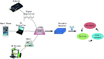
As the main advantage of μPADs is compact and low-cost, we suggest that three kinds of technology could be utilized to develop the prototype of μPADs-based instruments rapidly, including open source hardware-Aduino,62 smart phone and 3D printing, as shown in Fig. 10. As an open source hardware, Arduino has be used widely in many areas as a compact data collecting and processing unit. Many sensor interfaces have been developed and modularized. If μPADs are designed as chemical or bio sensors to adapt the Arduino interfaces, the powerful resources of open source hardware can be utilized to accelerate the development of μPADs. In the near future, almost everyone can own a smart phone. Smart phone can be used as a powerful pocket computer to analyze the detecting data, which can be gathered from its camera or from Arduino. With the networking of smart phone, the instruments can realize “on-site detection” and “off-site diagnosis”. Now the desktop 3D printers are very cheap and many of them can be purchased within $200–$1000. It can be a low-cost and powerful tool to rapidly fabricate the mechanical structures of instruments. In our previous study,63 we demonstrated that each doctor or patient can fabricate customized prostheses at clinic with a low cost. Also μPADs researchers deserve to have desktop printers in their own labs as the fabrication assistants.
 |
| Fig. 10 Possible constituents of μPAD-based instruments. | |
4.5 Future directions
Large-scale printing is commonly used in the process of images and text replication, which includes flexographic printing, screen printing, inkjet printing, offset printing, typography, rotogravure and rocking plate printing et al. So far, various large-scale printing methods have been used to fabricate μPADs, such as flexographic printing, screen printing, inkjet printing and so on. As a mass production method, we believe that more kinds of printing methods will be used to fabricate μPADs in the near future. Take rotogravure as an example, the ink in the gravure can be replaced by other hydrophobic reagents as needed, and the paper can be replaced by the filter paper. Thus, the printed areas will become hydrophobic when printed as usual. In a word, other large-scale printing methods might be the developing direction of μPADs fabrication. What's more, the manufacturing of μPADs will move in the direction of low cost, high resolution and easy fabrication.
While μPADs have so multiple applications and have been developed rapidly, there are still many problems which need to be solved. For example, the form of paper μPADs based is rather limited. Researchers need to find other porous materials to improve this situation. The low cost, easy using and good biological compatibility enable μPADs to enjoy a wide range of applications in future. As this review is focused on the fabrication method of μPADs, researchers are encouraged to read more related reviews in their interested area, which is shown in Table 3.
Table 3 Proposed reviews on μPADs
Area/subject |
Contents |
Ref no. |
Publication year |
General |
Progress of μPAD until 2012 |
64 |
2012 |
Progress of μPAD, especially from October 2012 to October 2014 |
55 |
2014 |
Point-of-care |
Challenges to commercialization of POC |
65 |
2012 |
Progress of POC until 2014 |
66 |
2014 |
Sensor |
Nanobiosensors for diagnostics |
67 |
2013 |
Sensor for optical and electrochemical detection |
68 |
2013 |
Paper electrodes for bioelectrochemistry |
69 |
2015 |
5. Conclusion
In this review we have presented the current fabrication methods for 2D and 3D paper-based microfluidic analysis devices. In addition, we compare and analyze the resolution and cost of these fabrication methods. A variety of rapid, simple and low-cost μPADs fabrication methods have appeared of late as reported in the literature. However, μPADs are still in the laboratory research stage of development. We believe that the μPADs fabrication techniques will mature and μPADs will be applied to many kinds of testing and analysis fields in the near future.
Acknowledgements
This paper is sponsored by the Science Fund for Creative Research Groups of National Natural Science Foundation of China (no. 51221004), National Natural Science Foundation of China (no. 51375440), Public Technology Research Program of Zhejiang Province (no. 2015C31062). The referees' professional suggestions are appreciated.
References
- A. W. Martinez, S. T. Phillips, M. J. Butte and G. M. Whitesides, Patterned paper as a platform for inexpensive, low-volume, portable bioassays, Angew. Chem., Int. Ed., 2007, 46, 1318–1320 CrossRef CAS PubMed.
- Y. Lu, W. Shi, L. Jiang, J. Qin and B. Lin, Rapid prototyping of paper-based microfluidics with wax for low-cost, portable bioassay, Electrophoresis, 2009, 30, 1497–1500 CrossRef CAS PubMed.
- E. Carrilho, A. W. Martinez and G. M. Whitesides, Understanding wax printing: a simple micropatterning process for paper-based microfluidics, Anal. Chem., 2009, 81, 7091–7095 CrossRef CAS PubMed.
- K. M. Schilling, A. L. Lepore, J. A. Kurian and A. W. Martinez, Fully enclosed microfluidic paper-based analytical devices, Anal. Chem., 2012, 84, 1579–1585 CrossRef CAS PubMed.
- T. Songjaroen, W. Dungchai, O. Chailapakul and W. Laiwattanapaisal, Novel, simple and low-cost alternative method for fabrication of paper-based microfluidics by wax dipping, Talanta, 2011, 85, 2587–25933 CrossRef CAS PubMed.
- A. Zhang and Y. Zha, Fabrication of paper-based microfluidic device using printed circuit technology, AIP Adv., 2012, 022171 CrossRef PubMed.
- D. A. Bruzewicz, M. Reches and G. M. Whitesides, Low-cost printing of poly(dimethylsiloxane) barriers to define microchannels in paper, Anal. Chem., 2008, 80, 3387–3392 CrossRef CAS PubMed.
- J. Nie, Y. Zhang, L. Lin, C. Zhou, S. Li, L. Zhang and J. Li, Low-cost fabrication of paper-based microfluidic devices by one-step plotting, Anal. Chem., 2012, 84, 6331–6335 CrossRef CAS PubMed.
- K. Abe, K. Suzuki and D. Citterio, Inkjet-printed microfluidic multianalyte chemical sensing paper, Anal. Chem., 2008, 80, 6928–6934 CrossRef CAS PubMed.
- K. Abe, K. Kotera, K. Suzuki and D. Citterio, Inkjet-printed paperfluidic immune-chemical sensing device, Anal. Bioanal. Chem., 2010, 398, 885–893 CrossRef CAS PubMed.
- J. Olkkonen, K. Lehtinen and T. Erho, Flexographically printed fluidic structures in paper, Anal. Chem., 2010, 82, 10246–10250 CrossRef CAS PubMed.
- G. Chitnis, Z. Ding, C. Chang, C. A. Savran and B. Ziaie, Laser-treated hydrophobic paper: an inexpensive microfluidic platform, Lab Chip, 2011, 11, 1161–1165 RSC.
- P. Spicar-Mihalic, B. Toley, J. Houghtaling, T. Liang, P. Yager and E. Fu, CO2 laser cutting and ablative etching for the fabrication of paper-based devices, J. Micromech. Microeng., 2013, 23, 067003 CrossRef.
- J. Nie, Y. Liang, Y. Zhang, S. Le, D. Li and S. Zhang, One-step patterning of hollow microstructures in paper by laser cutting to create microfluidic analytical devices, Analyst, 2013, 138, 671–676 RSC.
- V. F. Curto, N. Lopez-Ruiz, L. F. Capitan-Vallvey, A. J. Palma, F. Benito-Lopez and D. Diamond, Fast prototyping of paper-based microfluidic devices by contact stamping using indelible ink, RSC Adv., 2013, 3, 18811–18816 RSC.
- P. T. Garcia, T. M. G. Cardoso, C. D. Garcia, E. Carrilho and W. K. T. Coltro, A handheld stamping process to fabricate microfluidic paper-based analytical devices with chemically modified surface for clinical assays, RSC Adv., 2014, 4, 37637–37644 RSC.
- Y. He, Y. Wu, X. Xiao, J. Fu and G. Xue, A low-cost and rapid microfluidic paper-based analytical device fabrication method: flash foam stamp lithography, RSC Adv., 2014, 4, 63860–63865 RSC.
- E. M. Fenton, M. R. Mascarenas, G. P. Lopez and S. S. Sibbett, Multiplex lateral-flow test strips fabricated by two-dimensional shaping, ACS Appl. Mater. Interfaces, 2009, 1, 124–129 CAS.
- L. Christopher, Z. Cassano and H. Fan, Laminated paper-based analytical devices (LPAD): fabrication, characterization, and assays, Microfluid. Nanofluid., 2013, 15, 173–181 CrossRef.
- D. L. Giokas, G. Z. Tsogas and A. G. Vlessidis, Programming fluid transport in paper-based microfluidic devices using razor-crafted open channels, Anal. Chem., 2014, 86, 6202–6207 CrossRef CAS PubMed.
- A. C. Glavan, R. V. Martinez, E. J. Maxwell, A. B. Subramaniam, R. M. D. Nunes, S. Soh and G. M. Whitesides, Rapid fabrication of pressure-driven open-channel microfluidic devices in omniphobic RF paper, Lab Chip, 2013, 13, 2922–2930 RSC.
- C. Renault, X. Li, S. E. Fosdick and R. M. Crooks, Hollow-channel paper analytical devices, Anal. Chem., 2013, 85, 7976–7979 CrossRef CAS PubMed.
- M. M. Thuo, R. V. Martinez, W. Lan, X. Liu, J. Barber, M. B. J. Atkinson, D. Bandarage, J. Bloch and G. M. Whitesides, Fabrication of low-cost paper-based microfluidic devices by embossing or cut-and-stack methods, Chem. Mater., 2014, 26, 4230–4237 CrossRef CAS.
- T. Nurak, N. Praphairaksit and O. Chailapakul, Fabrication of paper-based devices by lacquer spraying method for the determination of nickel (II) ion in waste water, Talanta, 2013, 114, 291–296 CrossRef CAS PubMed.
- W. Dungchai, O. Chailapakul and C. S. Henry, A low-cost, simple, and rapid fabrication method for paper-based microfluidics using wax screen-printing, Analyst, 2011, 136, 77–82 RSC.
- Y. Sameenoi, P. N. Nongkai, S. Nouanthavong, C. S. Henry and D. Nacapricha, One-step polymer screen-printing for microfluidic paper-based analytical device (μPAD) fabrication, Analyst, 2014, 139, 6580–6588 RSC.
- A. W. Martinez, S. T. Phillips, B. J. Wiley, M. Gupta and G. M. Whitesides, FLASH: a rapid method for prototyping paper-based microfluidic devices, Lab Chip, 2008, 8, 2146–2150 RSC.
- E. Carrilho, S. T. Phillips, S. J. Vella, A. W. Martinez and G. M. Whitesides, Paper microzone plates, Anal. Chem., 2009, 81, 5990–5998 CrossRef CAS PubMed.
- Q. He, C. Ma, X. Hu and H. Chen, Method for fabrication of paper-based microfluidic devices by alkylsilane self-assembling and UV/O3-patterning, Anal. Chem., 2013, 85, 1327–1331 CrossRef CAS PubMed.
- Y. He, W. Wu and J. Fu, Rapid fabrication of paper-based microfluidic analytical devices with desktop stereolithography 3D printer, RSC Adv., 2015, 5, 2694–2701 RSC.
- L. OuYang, C. Wang, F. Du, T. Zheng and H. Liang, Electrochromatographic separations of multicomponent metal complexes on a microfluidic paper-based device with a simplified photolithography, RSC Adv., 2014, 4, 1093–1101 RSC.
- J. Songok, M. Tuominen, H. Teisala, J. Haapanen, J. Mäkelä, J. Kuusipalo and M. Toivakka, Paper-based microfluidics: fabrication technique and dynamics of capillary-driven surface flow, ACS Appl. Mater. Interfaces, 2014, 6, 20060 CAS.
- C. L. Sones, I. N. Katis, P. J. W. He, B. Mills, M. F. Namiq, P. Shardlow, M. Ibsen and R. W. Eason, Laser-induced photo-polymerisation for creation of paper-based fluidic devices, Lab Chip, 2014, 14, 4567–4574 RSC.
- P. J. W. He, I. N. Katis, R. W. Eason and C. L. Sones, Laser-based patterning for fluidic devices in nitrocellulose, Biomirofluidics, 2015, 9, 026503 CrossRef PubMed.
- X. Li, J. Tian, T. Nguyen and W. Shen, Paper-based microfluidic devices by plasma treatment, Anal. Chem., 2008, 80, 9131–9134 CrossRef CAS PubMed.
- P. Kao and C. Hsu, One-step rapid fabrication of paper-based microfluidic devices using fluorocarbon plasma polymerization, Microfluid. Nanofluid., 2014, 16, 811–818 CrossRef CAS.
- C. G. Obeso, M. P. Sousa, W. Song, M. A. Rodriguez-Pérez, B. Bhushan and J. F. Mano, Modification of paper using polyhydroxybutyrate to obtain biomimetic superhydrophobic substrates, Colloids Surf., A, 2013, 416, 51–55 CrossRef PubMed.
- X. Li, J. Tian, G. Garnier and W. Shen, Fabrication of paper-based microfluidic sensors by printing, Colloids Surf., B, 2010, 76, 564–570 CrossRef CAS PubMed.
- J. Wang, M. R. N. Monton, X. Zhang, C. D. M. Filipe, R. Pelton and J. D. Brennan, Hydrophobic sol-gel channel patterning strategies for paper-based microfluidics, Lab Chip, 2014, 14, 691–695 RSC.
- K. Maejima, S. Tomikawa, K. Suzuki and D. Citterio, Inkjet printing: an integrated and green chemical approach to microfluidic paper-based analytical devices, RSC Adv., 2013, 3, 9258–9263 RSC.
- P. Kwong and M. Gupta, Vapor phase deposition of functional polymers onto paper-based microfluidic devices for advanced unit operations, Anal. Chem., 2012, 84, 10129–10135 CrossRef CAS PubMed.
- P. D. Haller, C. A. Flowers and M. Gupta, Three-dimensional patterning of porous materials using vapor phase polymerization, Soft Matter, 2011, 7, 2428–2432 RSC.
- G. Demirel and E. Babur, Vapor-phase deposition of polymers as a simple and versatile technique to generate paper-based microfluidic platforms for bioassay applications, Analyst, 2014, 139, 2326–2331 RSC.
- B. Chen, P. Kwong and M. Gupta, Patterned fluoropolymer barriers for containment of organic solvents within paper-based microfluidic devices, ACS Appl. Mater. Interfaces, 2013, 5, 12701–12707 CAS.
- L. Cai, C. Xu, S. Lin, J. Luo, M. Wu and F. Yang, A simple paper-based sensor fabricated by selective wet etching of silanized filter paper using a paper mask, Biomicrofluidics, 2014, 8, 056504 CrossRef PubMed.
- Y. Jiang, Study on fabrication of microfluidic paper-based analytical devices and manipulation of microfluidic flow in paper-based channels using a hand-held corona treater, Master thesis, ZheJiang University, HangZhou, China, 2014.
- A. W. Martinez, S. T. Phillips and G. M. Whitesides, Three-dimensional microfluidic devices fabricated in layered paper and tape, Proc. Natl. Acad. Sci. U. S. A., 2008, 105, 19606–19611 CrossRef CAS PubMed.
- C. Cheng, A. D. Mazzeo, J. Gong, A. W. Martinez, S. T. Phillips, N. Jain and G. M. Whitesides, Millimeter-scale contact printing of aqueous solutions using a stamp made of paper and tape, Lab Chip, 2010, 10, 3201–3205 RSC.
- A. W. Martinez, S. T. Phillips, Z. Nie, C. Cheng, E. Carrilho, B. J. Wiley and G. M. Whitesides, Programmable diagnostic devices made from paper and tape, Lab Chip, 2010, 10, 2499–2504 RSC.
- G. G. Lewis, M. J. Ditucci, M. S. Baker and S. T. Phillips, High throughput method for prototyping three-dimensional, paper-based microfluidic devices, Lab Chip, 2012, 12, 2630–2633 RSC.
- L. Xiao, X. Liu, R. Zhong, K. Zhang, X. Zhang, X. Zhou, B. Lin and Y. Du, A rapid, straightforward, and print house compatible mass fabrication method for integrating 3D paper-based microfluidics, Electrophoresis, 2013, 34, 3003–3007 CAS.
- H. Liu and R. M. Crooks, Three-dimensional paper microfluidic devices assembled using the principles of origami, J. Am. Chem. Soc., 2011, 133, 17564–17566 CrossRef CAS PubMed.
- L. Ge, S. Wang, X. Song, S. Ge and J. Yu, 3D origami-based multifunction0integrated immunodevice: low-cost and multiplexed sandwich chemiluminescence immunoassay on microfluidic paper-based analytical device, Lab Chip, 2012, 12, 3150–3158 RSC.
- Y. Koo, J. Sankar and Y. Yun, High performance magnesium anode in paper-based microfluidic battery, powering on-chip fluorescence assay, Biomicrofluidics, 2014, 8, 054104 CrossRef PubMed.
- D. M. Cate, J. A. Adkins and J. Mettakoonpitak, et al., Recent Developments in Paper-Based Microfluidic Devices, Anal. Chem., 2014, 87(1), 19–41 CrossRef PubMed.
- J. L. Osborn, B. Lutz and E. Fu, et al., Microfluidics without pumps: reinventing the T-sensor and H-filter in paper networks, Lab Chip, 2010, 10(20), 2659–2665 RSC.
- P. Kauffman, E. Fu and B. Lutz, et al., Visualization and measurement of flow in two-dimensional paper networks, Lab Chip, 2010, 10(19), 2614–2617 RSC.
- E. Fu, B. Lutz and P. Kauffman, et al., Controlled reagent transport in disposable 2D paper networks, Lab Chip, 2010, 10(7), 918–920 RSC.
- B. J. Toley, B. McKenzie and T. Liang, et al., Tunable-Delay Shunts for Paper Microfluidic Devices, Anal. Chem., 2013, 85(23), 11545–11552 CrossRef CAS PubMed.
- H. Noh and S. T. Phillips, Metering the capillary-driven flow of fluids in paper-based microfluidic devices, Anal. Chem., 2010, 82(10), 4181–4187 CrossRef CAS PubMed.
- I. Jang and S. Song, Facile and precise flow control for a paper-based microfluidic device through varying paper permeability, Lab Chip, 2015, 15(16), 3405–3412 RSC.
- https://www.arduino.cc.
- Y. He, G. H. Xue and J. Z. Fu, Fabrication of low cost soft tissue prostheses with the desktop 3D printer, Sci. Rep., 2014, 4, 6973 CrossRef PubMed.
- D. R. Ballerini, X. Li and W. Shen, Patterned paper and alternative materials as substrates for low-cost microfluidic diagnostics, Microfluid. Nanofluid., 2012, 13(5), 769–787 CrossRef.
- C. D. Chin, V. Linder and S. K. Sia, Commercialization of microfluidic point-of-care diagnostic devices, Lab Chip, 2012, 12(12), 2118–2134 RSC.
- J. Hu, S. Q. Wang and L. Wang, et al., Advances in paper-based point-of-care diagnostics, Biosens. Bioelectron., 2014, 54, 585–597 CrossRef CAS PubMed.
- C. Parolo and A. Merkoçi, Paper-based nanobiosensors for diagnostics, Chem. Soc. Rev., 2013, 42(2), 450–457 RSC.
- E. W. Nery and L. T. Kubota, Sensing approaches on paper-based devices: a review, Anal. Bioanal. Chem., 2013, 405(24), 7573–7595 CrossRef CAS PubMed.
- C. Desmet, C. A. Marquette and L. J. Blum, et al., Paper electrodes for bioelectrochemistry: Biosensors and biofuel cells, Biosens. Bioelectron., 2015 DOI:10.1016/j.bios.2015.06.052.
|
This journal is © The Royal Society of Chemistry 2015 |
Click here to see how this site uses Cookies. View our privacy policy here.