Lingqiang Mengabc,
Hui Wangabc,
Xiaofang Weiabc,
Xiaopeng Lvd,
Ying Wang*ab and
Pengfei Wangab
aKey Laboratory of Photochemical Conversion and Optoelectronic Materials, Technical Institute of Physics and Chemistry, Chinese Academy of Sciences, Beijing, 100190, China. E-mail: wangy@mail.ipc.ac.cn; wangpf@mail.ipc.ac.cn
bKey Laboratory of Photochemical Conversion and Optoelectronic Materials and CityU-CAS Joint Laboratory of Functional Materials and Devices, Technical Institute of Physics and Chemistry, Chinese Academy of Sciences, Beijing, 100190, China
cUniversity of Chinese Academy of Sciences, Beijing, 100049, China
dSoochow University, Jiangsu Province, China
First published on 1st July 2015
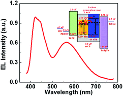
Multi-emissive layered white organic light-emitting diodes (WOLEDs) based on a blue fluorescent emitter and a yellow thermally activated delayed fluorescent emitter were constructed with the co-host of mCP. The WOLEDs afforded a color coordination of (0.34, 0.34), low efficiency roll-off, and a maximum external quantum efficiency of 4.7%.
Recently, pure organic thermally activated delayed fluorescence (TADF) emitters were developed as the new high efficiency fluorescent emitters, which both singlet and triplet can be harvested for light emission to achieve close to 100% internal quantum efficiency by the spin up-conversion process from triplet state to singlet state.11 Lee's group reported high efficiency hybrid WOLED combining a green TADF emitting material with red/blue phosphorescent emitting materials. A high EQE above 20% has been achieved in the hybrid WOLED, which is comparable to those of phosphorescent WOLEDs.12 Thus, the TADF emitter have the great potential to be used as the emitters for high efficiency WOLEDs with excellent stability. Adachi's group pioneered the high efficient organic fluorescent WOLEDs based on TADF emitters. The WOLEDs with the maximum luminescence of 9800 cd m−2 can be turn on at about 5 V, and the performance of the devices are among the highest of traditional pure organic fluorescent WOLEDs, with current efficiency of 16.7 cd A−1, EQE of 6.7% and CIE of (0.32, 0.39).13 Recently, they reported a white TADF-assisted fluorescence (TAF)-OLEDs with a high EQE of over 12% and CIE coordinates of (0.25, 0.31), which contains a blue TADF molecule as a common exciton donor and red/green classical fluorescent molecules as exciton acceptors.14 Nevertheless, the reported pure organic fluorescent WOLEDs are still rare, and the performance of the devices are still limited. The reported WOLEDs based on TADF emitters always show high efficiency at very low current density and luminance, and cannot satisfy the application in display and lighting.
Our group reported a novel TADF emitter of TXO–TPA, and the devices based on TXO–TPA gave yellow electroluminescence centred at 552 nm with color coordinates of CIE (0.45, 0.53).15 The yellow OLEDs exhibited very high efficiency without any light out-coupling enhancement, and TXO–TPA can be possibly used for the construction of WOLED combining with blue fluorescent emitters. In this communication, high efficiency pure organic fluorescence WOLEDs were developed incorporating a yellow TADF emitter and blue fluorescent emitter. Two separated yellow and blue emitting layers were used for the fabrication of the pure organic fluorescent WOLEDs. The optimized device exhibits good EL performance with a turn-on voltage of 4 V. The maximum EQE, current efficiency and power efficiency of the device are 4.4%, 10.9 cd A−1, and 8.5 lm W−1, which are better than those of the WOLED base on pure fluorescent emitters.
To develop a high efficiency white OLED with high CRI, a blue emitter with high fluorescent quantum yield (ηPL) are indispensable. Here 4P-NPB was used as the fluorescent blue emitter due to its high ηPL of 92%. TXO–TPA was chosen as the orange dopant. mCP was chosen as the host for the reasons following: (i) the high triplet energy level to confine the triplet excitons on the emitters, (ii) an appropriate ionization potential and electron affinity to adjust the carrier balance of holes and electrons in the emissive layer. In order to reduce the structural heterogeneity and facilitate charge transport between the two adjacent emitting layers, mCP was used as a common host for all lumophores. The device structure of the WOLEDs, the chemical structure and the energy level of the materials used are shown in Fig. 1. As shown in Fig. 1, these two primary-color emitters were arranged with a sequence of yellow-blue from the anode to the cathode. To transfer the energy of singlet excitons from mCP to 4P-NPB, a large spectral overlap between the ground state absorption of the exciton acceptor and fluorescent emission of the exciton donor is required. Fig. 2 shows the absorption spectra of TXO–TPA and 4P-NPB and the PL spectrum of mCP. The film of mCP shows two sharp emission peaks centered at 364 and 350 nm with a long tail. Thin films of 4P-NPB exhibits a rather broad absorption peak with a full width at half-maximum of 82 nm and peak wavelength of 362 nm. Thus, singlet energy from mCP is expected to be transferred to S1 of the 4P-NPB via a Förster process after the optically or electrically excitation of mCP molecules. Similar spectra overlap between the PL spectrum of mCP and the absorption of TXO–TPA can also be observed.
Excitons are formed on the mCP host with a singlet-to-triplet formation ratio (1:
3). Singlet excitons are transferred following a Förster resonant process onto the doped blue fluorophore of 4P-NPB for blue light (as shown in Fig. 2). While, the host triplets can migrate from the 4P-NPB:mCP layer to the TXO–TPA:mCP layer and efficiently transfer to the TXO–TPA by Dexter transfer process in that the non-radiative host triplets typically have long diffusion lengths (∼100 nm). Thus, TXO–TPA can emit yellow light by the efficient up-conversion from triplet to singlet (as shown in Fig. 2). Although there are some unavoidable loss in these transfer process, high efficient WOLEDs with the potential for unity internal quantum efficiency can be expected in the device structure since both singlet and triplet excitons can be utilized along independent channels. The balance of yellow emission and blue emission by the dedicate management of singlet and triplet excitons in the two emitting layers will be the key for the efficient WOLEDs (as shown in Fig. 2).
As we had demonstrated high efficient yellow OLEDs based on TXO–TPA with the concentration of 5 ± 1 wt%, the TXO–TPA concentration will be kept in the yellow emitting layer here. We first optimized the concentration of 4P-NPB in the blue emission layer. The doping concentration of 4P-NPB was changed from 0.5% to 20%, and the performance of all devices with different doping concentrations of 4P-NPB are summarized in Table 1. All these devices exhibited a turn-on voltage of 4 V. The device with a doping concentration of 0.5 wt% emits only yellow light with an emission peak of 552 nm and a color coordinate (0.39, 0.51). With increasing the 4P-NPB concentration, the blue emission from 4P-NPB appears and the intensities of these peaks increase. The color coordinate shifts from yellow light region into white light region. Since mCP is a hole transporting materials with a high hole mobility of 1.2 × 10⁻⁴ cm2 V−1 s−1, which is three times higher than that of electron mobility (4 × 10⁻⁵ cm2 V−1 s−1).16 And the hole mobility of 4P-NPB is also significantly higher than the electron mobility (μh = 6.6 × 10⁻⁴ cm2 V−1 s−1 and μe = 3.6 × 10⁻⁸ cm2 V−1 s−1).17 The exciton generation zone should be located at the 4P-NPB:mCP/TmPyPB interface. At the low doping concentration, the majority of the singlet excitons in the exciton generation zone will not decay on the 4P-NPB molecules, resulting in the blue emission. As the Förster distance of mCP and TXO–TPA is short, the singlet excitons also cannot effectively reach TXO–TPA via Förster resonant process and lead to the yellow emission. Thus, the efficiency of the device with the doping concentration of 0.5 wt% is inferior, markedly lower than that of OLEDs with only TXO–TPA as an emitter (ηEQE = 18%). When the doping concentration of 4P-NPB increases from 0.5 wt% to 2 wt%, the performance of the device remarkably increases due to the effective exploitation of the singlet excitons by 4P-NPB. While, the similar triplet energy of 4P-NPB (2.3 eV) compared to that of TXO–TPA (2.27 eV) leads to a possible Dexter energy transfer from the triplet state of TXO–TPA to the lower lying no-radiative triplet state of 4P-NPB, resulting in energy loss and thus a reduction in device efficiency. Thus, further increasing the doping concentration, the performance of the devices decrease because 4P-NPB can also be the trapping centers of triplet excitons. The device with a doping concentration of 2 wt% exhibits the highest performance with stable EL spectra, and the electroluminescence characteristics of the warm WOLEDs were shown in Fig. 3. The device affords a current efficiency of 10.9 cd A−1, a power efficiency of 8.5 lm W−1, and EQE of 4.4%, which are comparable with those of the devices based on fluorescent and phosphorescent emitters with similar structure.3 As lighting sources are generally characterized by their total emitting power, the maximum total efficiencies of the devices can be up to 18.5 cd A−1, 14.5 lm W−1, and 7.5%. From EL spectrum, it is clear that the sufficient blue emission for the warm WOLEDs can be achieved at low concentration of 4P-NPB. Notably, the EL spectra are independent of the applied voltage and there were no derivation or new peaks even at high voltage up to 10 V. As the low doping concentration of 4P-NPB, the generated triplet excitons cannot be efficiently transfer to 4P-NPB by Dexter energy transfer process. Consequently, it can be inferred that the triplet excitons will diffused into the TXO–TPA:mCP layer. To further get the strong evidence for the diffusion of triplet excitons to the TXO–TPA:mCP layer, the devices with structure of ITO/PEDOT (20 nm)/TAPC (30 nm)/TPA (0.5 nm)/mCP (x nm)/4P-NPB (0.5 nm)/mCP (10 nm)/TmPyPB (50 nm)/LiF (0.9 nm)/Al (100 nm) (x = 0, 3, and 10 nm) were fabricated. When there is no spacer between TXO–TPA and 4P-NPB, there is barely the emission from TXO–TPA can be observed (as shown in Fig. 4). Inserting a thin layer of mCP spacer, the emission from 4P-NPB appears and the intensity of the emission from 4P-NPB increases with the spacer thickness, providing a well-established proof for the diffusion (as shown in Fig. 4).18
Doping concentration of 4P-NPB | Maximum values | Color coordinate at 6 V | |||
---|---|---|---|---|---|
Turn-on voltage (V) | Current efficiency (cd A−1) | Power efficiency (lm W−1) | EQE (%) | ||
0.5% | 4 | 5.6 | 2.9 | 2.0 | (0.39, 0.51) |
2% | 4 | 10.9 | 8.5 | 4.4 | (0.37, 0.42) |
5% | 4 | 7.2 | 5.7 | 3.6 | (0.31, 0.35) |
10% | 4.1 | 4.9 | 2.4 | 2.5 | (0.30, 0.33) |
20% | 4 | 3.2 | 1.5 | 1.9 | (0.27, 0.27) |
To enhance the blue emission of the devices and shift the color coordination to (0.33, 0.33), device I, II, and III are fabricated and the device structures are following: device I:ITO/PEDOT (20 nm)/TAPC (40 nm)/TPA:mCP (5%) (5 nm)/4P-NPB:mCP (2%) (5 nm)/TmPyPB (50 nm)/LiF(0.9 nm)/Al (100 nm); device II:ITO/PEDOT (20 nm)/TAPC (40 nm)/TPA:mCP (5%) (10 nm)/4P-NPB:mCP (2%) (10 nm)/TmPyPB (50 nm)/LiF (0.9 nm)/Al (100 nm); device III:ITO/PEDOT (20 nm)/TAPC (40 nm)/TPA:mCP (5%) (10 nm)/mCP (5 nm)/4P-NPB:mCP (2%) (10 nm)/TmPyPB (50 nm)/LiF (0.9 nm)/Al (100 nm). The performance of device I, II and III are summarized in Table 2. As expected, all devices showed white EL emission with intense blue emission. However, the performance of device I are obviously low: the maximum EQE of the device is only 1.8% and the emission from TXO–TPA is suppressed. This can be attributed the quenching effect of high density of triplet excitons in the narrow yellow emitting layer. Increasing the thickness of the light emitting layer, pronounced enhancement of the device performance can be observed for device II and III. As shown in Fig. 5, device II is turned on at 4 V with a color coordination of (0.34, 0.34). The maximum EQE, current efficiency, and power efficiency of the device are 4.7%, 8.1 cd A−1, and 6.4 lm W−1, respectively. Interestingly, low efficiency roll-off can also be observed, and the critical current density (jc) of the device, where EQE declines by half from its peak, is about 112 mA cm−2, which is higher than the reported multi-emissive layers WOLEDs based on phosphorescent emitters.18 An interlayer between the 4P-NPB:mCP and TXO–TPA:mCP layers is used to prevent mutual exciton transfer and quenching processes, which are indispensable for multi-emissive layers hybrid WOLED. Interestingly, device III exhibits similar performance and CIE to those of device II, indicating that the mutual quenching between 4P-NPB and TXO–TPA can be unconsidered, even mCP is not a bipolar host of 4P-NPB.
Device structure | Maximum values | Color coordinate at 6 V | |||
---|---|---|---|---|---|
Turn-on voltage (V) | Current efficiency (cd A−1) | Power efficiency (lm W−1) | EQE (%) | ||
Device I | 3.6 | 3.2 | 2.4 | 1.8% | (0.35, 0.32) |
Device II | 4.0 | 8.1 | 6.4 | 4.7% | (0.34, 0.34) |
Device III | 4.3 | 8 | 5.8 | 4.4% | (0.37, 0.36) |
Footnote |
† Electronic supplementary information (ESI) available: Materials, device fabrication and characterization. See DOI: 10.1039/c5ra09168c |
This journal is © The Royal Society of Chemistry 2015 |