
Graphene/SrTiO3 nanocomposites used as an effective electron-transporting layer for high-performance perovskite solar cells
Chen Wanga,
Ying Tanga,
Yajing Hua,
Lu Huanga,
Jianxun Fub,
Jing Jina,
Weimin Shia,
Linjun Wanga and
Weiguang Yang*a
aDepartment of Electronic Information Materials, School of Materials Science and Engineering, Shanghai University, Shanghai 200444, China. E-mail: wgyang@shu.edu.cn
bKey Laboratory of Modern Metallurgy and Materials Processing, School of Materials Science and Engineering, Shanghai University, Shanghai 200072, China
First published on 2nd June 2015
Abstract
Organic–inorganic perovskite solar cells based on binary oxides have been studied for a long time and have obtained an impressive advance in performance. However, studies using ternary oxides as the electron-transporting layer are scarce and there are still many problems to be solved. The ternary oxide SrTiO3 with a perovskite structure is well matched with the perovskite absorber layer in the crystal structure. Although the device based on mesoporous-SrTiO3 (mp-SrTiO3) showed a high Voc, its average Jsc is still too low compared with mp-TiO2 based devices. In this work, we used graphene/SrTiO3 nanocomposites as an effective electron-transporting layer. Due to the superconductivity of the graphene combined with tuning the amount of the starting graphene to increase the light harvesting of the absorber layer and decrease recombination centers, we got a great achievement. The device based on graphene/SrTiO3 nanocomposites exhibited a PCE of 10% with a Jsc of 18.08 mA cm−2, increased by 46.0 and 45.6% respectively compared with the mp-SrTiO3 based device, indicating incorporation of graphene is an effective way to improve the Jsc of mp-SrTiO3 based perovskite solar cells.
1. Introduction
As a promising new energy technology, organic–inorganic perovskite solar cells as third generation solar cells have been attracting a wide range of attention in recent years due to their traits of direct band gap, large absorption coefficient, ambipolar diffusion and long carrier diffusion length.1–3 The power conversion efficiency (PCE) of this kind of solar cell was expected to be up to 20%,4 and a highest PCE of 19.3% has already been achieved.5 Mesoporous-TiO2 (mp-TiO2) as an anode material is the most common device architecture in perovskite solar cells. This mp-TiO2 as an electron-transporting layer extracts photoexcited electrons generated in the absorber layer.6 The most used nanostructures in constructing perovskite solar cells were anatase TiO2 nanoparticles, with the highest power conversion efficiency (PCE) of over 17%. Compared with the anatase TiO2 nanoparticles-based device, the rutile TiO2 nanoparticles-based device possesses the properties of higher electron diffusion coefficient and lower electron recombination demonstrating a PCE close to 15%.7 In addition, nanosheets,8–10 nanorods,11–15 nanotubes,16 nanowires17–20 and mesoporous single crystals21 were also used in the devices based on mp-TiO2, and no matter what shape they were, their device performances were dramatically affected by the thickness of the mp-TiO2 layer. The perovskite solar cell showed a higher PCE when it had a thinner mp-TiO2 layer. Mp-ZnO is a most suitable candidate to replace the mp-TiO2 due to its characteristics of comparable energy levels as well as relatively higher electron mobility.22,23 Hagfeldt and co-workers reported a device based on mp-ZnO for the first time.24 They used ZnO nanorod arrays to fabricate an ITO/bl-ZnO/NRA-ZnO/MAPbI3/spiro-OMeTAD/Ag device, which achieved a PCE of 5%. Park and co-workers adjusted the diameter and length of the ZnO nanorod arrays improving the PCE to 11.13%.25 The most efficient device based on ZnO was made by Dianyi Liu and co-workers: the ZnO nanoparticles were assembled with CH3NH3PbI3, showing a PCE of 15.7%.26 Mp-Al2O3 as an insulating material worked only as a scaffold in the perovskite solar cell; the device based on mp-Al2O3 was called a “meso-superstructured solar cell”, which was first put forward by Snaith and coworkers.27 In this kind of device the photoexcited electrons were directly transported throughout the perovskite layer instead of injecting into Al2O3, which is totally different from TiO2.28 The device using mp-Al2O3 showed a higher Voc than the TiO2-based device. The device used the FTO/bl-TiO2/mp-Al2O3/MAPbBr3/PDI/Au structure and achieved a Voc as high as 1.3 V.29 Similar to mp-Al2O3, mp-ZrO2 (ref. 30 and 31) and SiO2 (ref. 32) are also ideal materials for the scaffold material and the device performance based on both of them showed a PCE over 10%.Compared to the binary oxides discussed above, ternary oxides such as SrTiO3 have been rarely reported with regards to perovskite solar cells. SrTiO3 possesses the perovskite structure, and provides lots of physical properties, including superconductivity,33 ferroelectricity,34 and thermoelectricity.35 Electron mobility of bulk SrTiO3 is 5–8 cm2 V s−1 at room-temperature,36 which is much higher than TiO2 (0.1–4 cm2 V s−1).37 Although the band gap of SrTiO3 is analogous to that of TiO2, its slightly higher conduction band is more suitable to CH3NH3PbI3, and due to its high dielectric constant, the charge recombination at the interface will be reduced to some extent. Ashok Bera and co-workers first reported a mp-SrTiO3 based perovskite solar cell, which showed a high Voc close to 1 V, and by adjusting the thickness of the mp-SrTiO3, a Voc > 1 V could be reliably achieved, which was at the cost of Jsc.38 Despite the relatively high Voc, its average Jsc is still too low compared with mp-TiO2 based devices. There is an urgent need to find an effective way to improve the Jsc of mesoporous-SrTiO3 (mp-SrTiO3) based perovskite solar cells.
Recently, graphene, equipped with unique properties such as excellent optical, thermal and electrical activities,39–42 has attracted lots of interest. Graphene–TiO2 composites have been successfully used as the anode material in both dye-sensitized solar cells and perovskite solar cells.43,44 Due to its high transparency and electron mobility, the performance of solar cells based on graphene–TiO2 composites has been dramatically improved.
In this work, we report the first use of graphene/SrTiO3 nanocomposites as the effective electron-transporting layer. Owing to its remarkably high charge mobility and electronic conductivity, graphene greatly improved the Jsc of mp-SrTiO3 based perovskite solar cells. The best performance we obtained of the solar cell based on graphene/SrTiO3 nanocomposites exhibited a PCE of 10%, and the short-circuit current density was boosted from 12.42 to 18.08 mA cm−2 after adjustment of the graphene content. We attributed the improvement in device performance to the fast electron transfer as well as the decrease in the recombination centers and the increase in the light harvesting of the absorber layer, indicating the incorporation of graphene is an effective way to enhance the Jsc of mp-SrTiO3 based perovskite solar cells.
2. Experimental
2.1 Materials
Titanium(IV)-n-butoxide (Ti(OBu)4) (99+%), tetra-n-butylammonium hydroxide (TBAH) (40 wt% in aqueous solution), strontium hydroxide octahydrate (Sr(OH)2·8H2O) (99%), diethylene glycol (DEG) (99%), and graphene were purchased from Alfa Aesar.2.2 Preparation of graphene/SrTiO3 samples
The graphene/SrTiO3 samples were synthesized by a solvothermal method. 20 ml DEG and 0.13 M Sr(OH)2·8H2O were added to a 50 ml beaker, which was heated to 50 °C and stirred for 2 h in an oil bath until all the Sr(OH)2·8H2O was dissolved, then 5 mg graphene was added to the obtained solution. It was put in an ultrasonic bath for approximately 2 h to disperse the graphene, this was followed by adding 0.18 M Ti(OBu)4, and stirring for 20 min with a magnetic stirrer. Next 4 ml TBAH was added to the solution, it was also stirred for 20 min, the final solution was transferred to Teflon cups in an autoclave held at 200 °C for 50 h. A series of nanocomposites of SrTiO3 with a varying amount of graphene were denoted as S, C5, C15, C25, C35, C45, according to the weight of graphene designated as 0 mg, 5 mg, 15 mg, 25 mg, 35 mg, 45 mg, respectively. All the samples were prepared in a similar manner. After cooling naturally to room temperature, the nanocomposites were collected by centrifugation and washed thoroughly with alcohol three times. Finally, ethylcellulose, lauric acid, and terpineol were added into the resulting products and milled for 2 h to obtain viscous pastes. The nominal composition of sample/terpineol/ethylcellulose/lauric acid was 1/6/0.3/0.1.2.3 Synthesis of CH3NH3I
CH3NH3I was prepared according to the reported procedure.45 CH3NH3I was synthesized by reacting 34 ml of methylamine (33% in ethanol) and 30 ml hydroiodic acid (57 wt% in water) in an ice bath for 2 h with stirring. The precipitate was recovered by putting the solution on a rotary evaporator and carefully removing the solvents at 50 °C. The precipitate was washed three times with diethyl ether and dried at 60 °C in a vacuum oven for 24 h.2.4 Solar cell fabrication
FTO glasses were etched with Zn powder and diluted HCl and washed by ultrasonication with deionized water, and ethanol. Then the cleaned substrates were coated with titanium diisopropoxide bis(acetylacetonate) (75% Aldrich) diluted in anhydrous ethanol (1![[thin space (1/6-em)]](https://www.rsc.org/images/entities/char_2009.gif) :39, volume ratio) by spin-coating to make a compact layer. Next TiO2 dense layers were sintered at 500 °C for 20 min. On the TiO2 compact layers, the graphene/SrTiO3 paste (diluted in anhydrous ethanol) was deposited by spin-coating at 4000 rpm for 30 s, and was annealed at 500 °C for 20 min to produce mp-graphene/SrTiO3 film. The prepared graphene/SrTiO3 films were coated with PbI2 (99% purity) from a solution of 1 mol L−1 PbI2 in dimethylformamide with a spin-coating speed of 7000 rpm for 30 s, followed by heating to 70 °C for 30 min. After the samples cooled to room temperature, 300 μl of 0.063 M CH3NH3I solution in 2-propanol was dropped on the PbI2-coated substrate loading for 30 s, which was spun at 5000 rpm for 30 s and dried at 100 °C for 15 min. Then the hole transport material (HTM) solution was coated on the FTO/compact TiO2/mp-graphene/SrTiO3/CH3NH3PbI3 substrates at 4000 rpm for 30 s. The composition of the HTM was 0.170 M 2,29,7,79-tetrakis-(N,N-di-p-methoxyphenylamine)-9,9-spirobifluorene (spiro-MeOTAD), 0.064 M bis(trifluoromethane)sulfonimide lithium salt (LiTFSI, 99.95%, Aldrich) and 0.198 M 4-tert-butylpyridine (TBP, 96%, Aldrich) in the mixed solvent of chlorobenzene (99.8%, Aldrich) and acetonitrile (99.8%, Aldrich) (chlorobenzene:acetonitrile = 1:0.1 v/v). Samples were left in a desiccator overnight and to finish the devices an 80 nm-thick Ag layer was deposited on top of the HTM layer by a thermal evaporation the next day. All device fabrication steps were carried out under the atmospheric environment.
:39, volume ratio) by spin-coating to make a compact layer. Next TiO2 dense layers were sintered at 500 °C for 20 min. On the TiO2 compact layers, the graphene/SrTiO3 paste (diluted in anhydrous ethanol) was deposited by spin-coating at 4000 rpm for 30 s, and was annealed at 500 °C for 20 min to produce mp-graphene/SrTiO3 film. The prepared graphene/SrTiO3 films were coated with PbI2 (99% purity) from a solution of 1 mol L−1 PbI2 in dimethylformamide with a spin-coating speed of 7000 rpm for 30 s, followed by heating to 70 °C for 30 min. After the samples cooled to room temperature, 300 μl of 0.063 M CH3NH3I solution in 2-propanol was dropped on the PbI2-coated substrate loading for 30 s, which was spun at 5000 rpm for 30 s and dried at 100 °C for 15 min. Then the hole transport material (HTM) solution was coated on the FTO/compact TiO2/mp-graphene/SrTiO3/CH3NH3PbI3 substrates at 4000 rpm for 30 s. The composition of the HTM was 0.170 M 2,29,7,79-tetrakis-(N,N-di-p-methoxyphenylamine)-9,9-spirobifluorene (spiro-MeOTAD), 0.064 M bis(trifluoromethane)sulfonimide lithium salt (LiTFSI, 99.95%, Aldrich) and 0.198 M 4-tert-butylpyridine (TBP, 96%, Aldrich) in the mixed solvent of chlorobenzene (99.8%, Aldrich) and acetonitrile (99.8%, Aldrich) (chlorobenzene:acetonitrile = 1:0.1 v/v). Samples were left in a desiccator overnight and to finish the devices an 80 nm-thick Ag layer was deposited on top of the HTM layer by a thermal evaporation the next day. All device fabrication steps were carried out under the atmospheric environment.
3. Results and discussion
The X-ray powder diffraction (XRD) patterns of as-prepared graphene/SrTiO3 nanocomposites with different solvothermal times at 200 °C are given in Fig. 1, which shows the crystalline SrTiO3 has a cubic perovskite structure. The peak centers for SrTiO3 were measured to be 22.66°, 32.30°, 39.86°, 46.38°, 52.22°, 57.68°, 67.70°, 72.54°, 77.08°, corresponding to the (100), (110), (111), (200), (210), (211), (220), (221), (310) crystal planes of SrTiO3 respectively, in agreement with the previous reports.46,47 The peaks at 25.20°, 36.42°, 44.12°, 49.94° originate from TiO2. With the increase in the reaction time, the peak intensity of TiO2 decreased while that of SrTiO3 increased, indicating that TiO2 was gradually converted to SrTiO3. When the reaction time was increased to 50 h, the peak of the byproduct could hardly be seen, showing that extremely pure SrTiO3 was synthesized. Due to the amount of graphene being too low to detect, the peak of the graphene did not appear in the XRD patterns.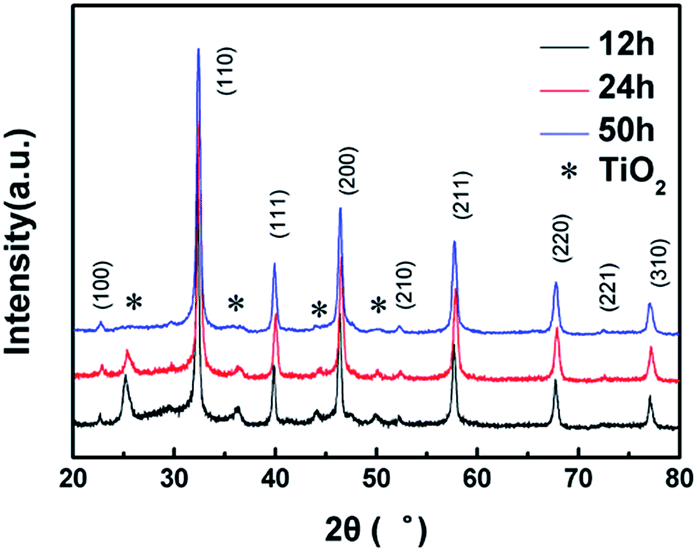 | ||
| Fig. 1 XRD patterns of graphene/SrTiO3 nanocomposites with different reaction times at 200 °C. The * in the figure indicates a peak of TiO2. | ||
Fig. 2 shows a scanning electron microscopy (SEM) image of the as-prepared graphene/SrTiO3 product diluted in ethanol and dropped on a Si substrate. The SrTiO3 nanoparticles adhered to the graphene flakes tightly, indicating the strong binding force between the graphene flakes and SrTiO3 nanoparticles, which is of great help for the use of graphene flakes as a highway for electron transportation and collection. Since the sample was made without any further processing, the clustering of the sample was problematic. In spite of the cluster, the outlines of both the graphene flake and SrTiO3 nanoparticle could still be seen clearly.
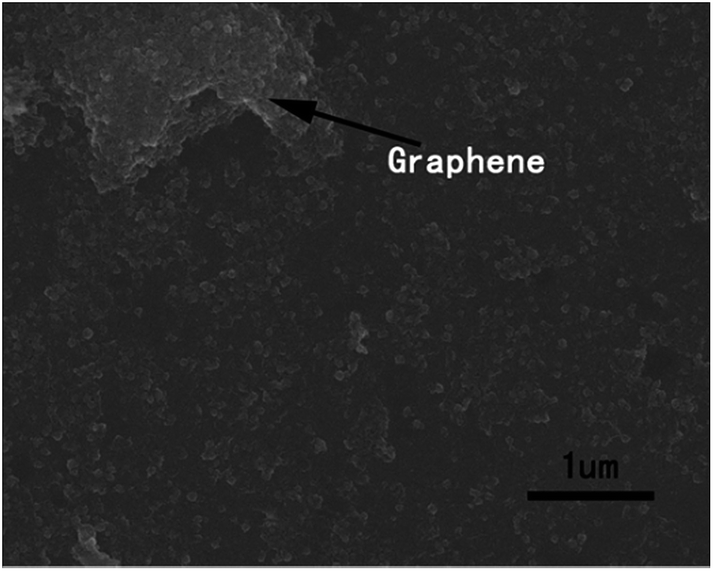 | ||
| Fig. 2 SEM image of graphene/SrTiO3 nanocomposites on Si substrate. | ||
Fig. 3a and b show transmission electron microscopy (TEM) and high resolution transmission electron microscopy (HRTEM) images of the graphene/SrTiO3 nanocomposites. It could be clearly observed that the graphene was monodispersed as nanosheets and SrTiO3 nanoparticles with diameters varying from 5–65 nm dispersed in the graphene nanosheet. The dotted circles in Fig. 3b represent SrTiO3 nanoparticles, adhering to the graphene nanosheet in a random way. The HRTEM image shown in Fig. 3c shows distinct lattice fringes. The fringe spacing was measured to be 0.39 nm and 0.28 nm, in line with the (001) and (110) planes of the cubic phase of SrTiO3, respectively. The regular crystal diffraction spots in the selected-area electron diffraction (SAED) pattern in Fig. 3d matched with cubic perovskite structure SrTiO3, indicating the good crystallinity of the SrTiO3.
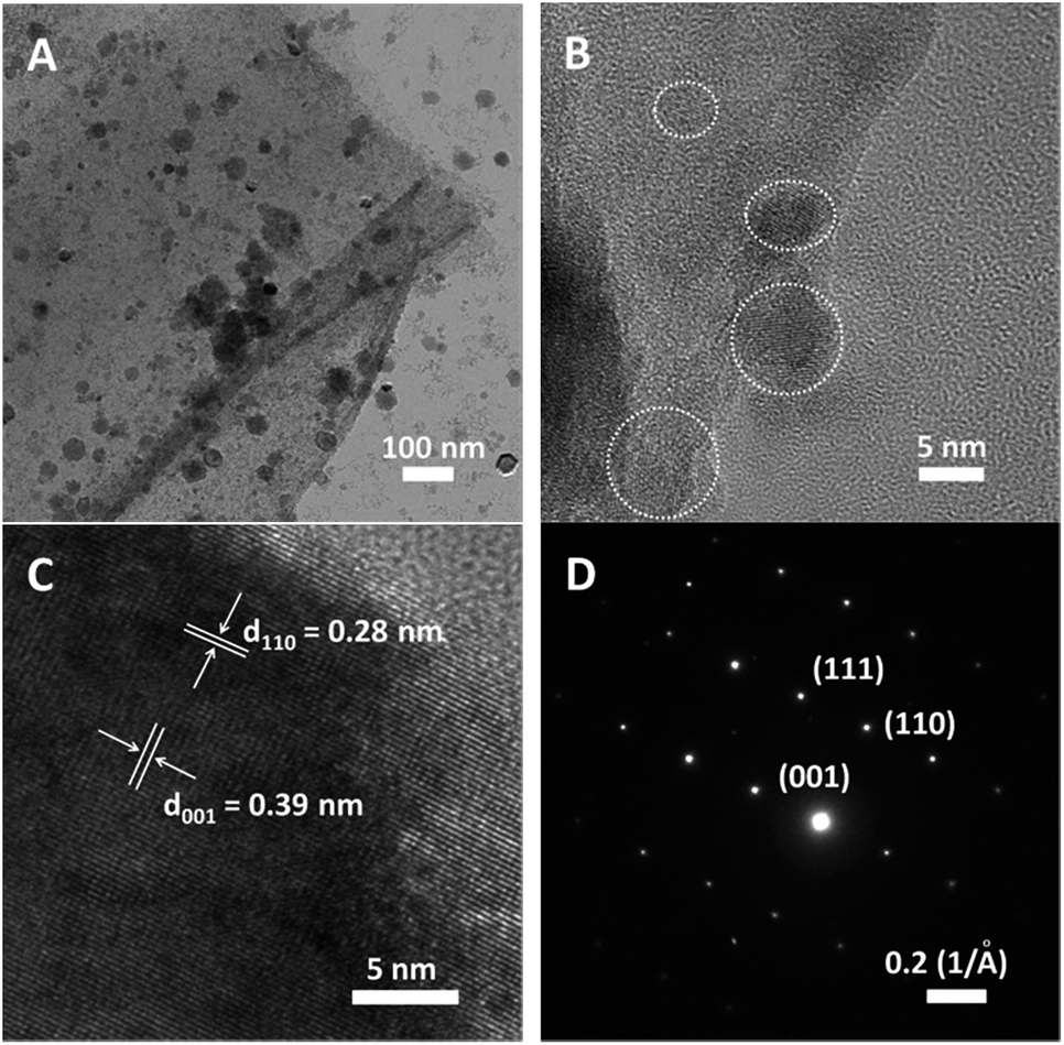 | ||
| Fig. 3 (A) TEM micrograph of graphene/SrTiO3 nanocomposites. (B) HRTEM image of graphene/SrTiO3 nanocomposites. (C) HRTEM image of SrTiO3 nanoparticle. (D) SAED pattern of SrTiO3 nanoparticle. | ||
Fig. 4 shows the XRD patterns for the CH3NH3PbI3 grown on a mp-graphene/SrTiO3 layer and a mp-TiO2 layer. The peaks at 14.20°, 20.15°, 23.35°, 24.61°, 28.50°, 31.90°, and 40.66° could be assigned to the (110), (112), (211), (202), (220), (312), and (224) crystal planes of the tetragonal perovskite structure CH3NH3PbI3 respectively, which was in good agreement with the previous work.48 There were no impurity peaks other than the ones attributable to CH3NH3PbI3 observed in the XRD patterns, suggesting that CH3NH3PbI3 grown on both the mp-graphene/SrTiO3 layer and mp-TiO2 layer was phase pure. While from the patterns it could be seen clearly that the intensities of three strong peaks of the CH3NH3PbI3 grown on the mp-graphene/SrTiO3 layer were stronger than those on the mp-TiO2 layer, indicting a better crystallization of the CH3NH3PbI3 grown on the mp-graphene/SrTiO3 layer compared to on the mp-TiO2 layer, which may be attributed to a similar crystal structure of the CH3NH3PbI3 and SrTiO3 particle and the bigger size of the SrTiO3 particle.
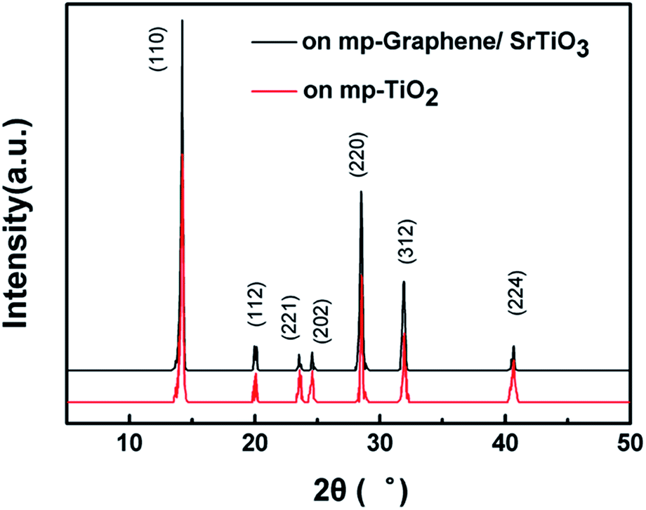 | ||
| Fig. 4 XRD patterns of the CH3NH3PbI3 grown on a mp-graphene/SrTiO3 layer and on a mp-TiO2 layer. | ||
Fig. 5 shows UV-vis transmission spectra of mp-graphene/SrTiO3 layers with different graphene content with the same thickness. The thickness of all the samples was 200 nm. As shown in Fig. 5, with increasing the graphene content, the transmittance of the mp-graphene/SrTiO3 layer decreased obviously. Despite the increase in graphene content, the transmittance is still over 85%, indicating the mp-graphene/SrTiO3 is suitable for being used as anode material.
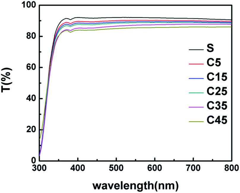 | ||
| Fig. 5 UV-vis transmission spectra of mp-graphene/SrTiO3 layers with different graphene content with the same thickness. | ||
Fig. 6 shows the UV-vis absorption spectra of CH3NH3PbI3 coated on mp-graphene/SrTiO3 layers and on a mp-TiO2 layer, the thickness of the mp-graphene/SrTiO3 layers and the mp-TiO2 layer was about 200 nm. It could be clearly seen that the CH3NH3PbI3 coated on mp-graphene/SrTiO3 could absorb most light in the visible region. In spite of the difference in graphene content, all the samples showed a similar trend in the UV-vis absorption spectra, and the absorbances of different samples were indistinguishable, indicating the strong light absorption of the CH3NH3PbI3 on the mp-graphene/SrTiO3 layer. Compared to the mp-TiO2 case, the absorbance of the CH3NH3PbI3 on the mp-graphene/SrTiO3 layer was higher when the wavelength was over 500 nm, although its absorbance at shorter wavelengths was slightly lower, meaning that the general absorption of the CH3NH3PbI3 coated on a mp-graphene/SrTiO3 layer was higher than that on a mp-TiO2 layer. Comparing Fig. 6 with Fig. 5, it could be easily concluded that with the increase in the graphene content, the absorbance of CH3NH3PbI3 decreased in fact, since the graphene absorbed part of the light.
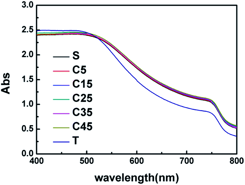 | ||
| Fig. 6 UV-vis absorption spectra of CH3NH3PbI3 on mp-graphene/SrTiO3 layers with different graphene content (S, C5, C15, C25, C35, C45) and on a mp-TiO2 layer (T). | ||
The current density–voltage (J–V) curves of the best performing cells of each series are shown in Fig. 7, their corresponding characteristic parameters are given in Table 1. It was obvious that the short-circuit current density and η increased with the increase in the graphene content, and with a further increase in the graphene content, the short-circuit current density and η dramatically decreased. Comparing S with T, it was obvious that the open-circuit voltage of S was higher than that of T, while the short-circuit current density of S was lower, despite the general absorption of the CH3NH3PbI3 coated on the mp-SrTiO3 layer being higher than that on the mp-TiO2 layer, which could be attributed to the less efficient carrier collection in the devices based on the mp-SrTiO3 layer. After adding the graphene to the mp-SrTiO3, the short-circuit current density was obviously improved and still maintained the higher open-circuit voltage. The short-circuit current density and η of C25 was 17.09 mA cm−2 and 9.41%, respectively, which increased by 37.6 and 37.3%, relative to S, respectively. Each series based on mp-graphene/SrTiO3 showed an open-circuit voltage over 0.90 V, and only changed slightly. So the improved performance was obviously attributed to the promoting effect of graphene, which greatly increased the Jsc of the device, due to its fast electron transfer. While with the further increase in the content of graphene, a dramatic decrease in Jsc appeared, which resulted from the decrease in absorbance of CH3NH3PbI3 and the increase in recombination of the carriers. As discussed above, with the increase in the density of graphene, the transmittance of the mp-graphene/SrTiO3 layer decreased, which resulted in the decrease in absorbance of CH3NH3PbI3, eventually reducing the amount of photo-generated carriers. What’s more, the introduction of conductive graphene will introduce new recombination centers and induce the lower photocurrent more or less, unless the graphene was fully coated with SrTiO3 nanoparticles without direct contact between the graphene and CH3NH3PbI3.49 However, the scale of the graphene flakes we made was very large, much larger than the thickness of the CH3NH3PbI3, and taking the aggregation of the graphene which leads to the graphene extending in any direction into account, therefore with the increase in the density of the graphene, there was unavoidable direct contact between graphene and CH3NH3PbI3. By comparing the FF of each series, a slight decrease could be seen, which could further confirm the presence of the new recombination centers introduced by graphene.
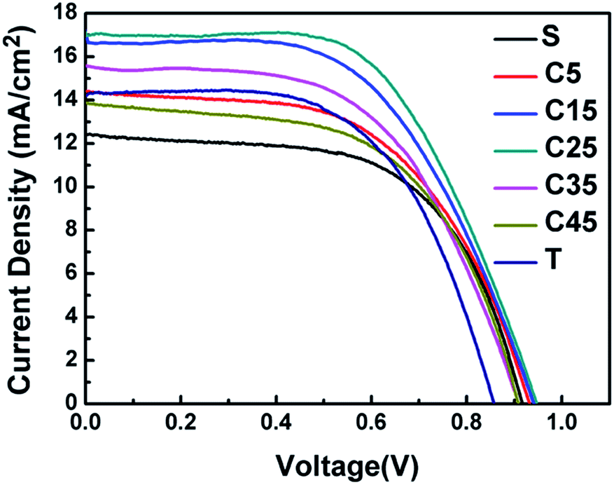 | ||
| Fig. 7 J–V characteristics of solar cells based on mp-graphene/SrTiO3 nanocomposites with different graphene content (S, C5, C15, C25, C35, C45) and on a mp-TiO2 layer (T) under simulated AM 1.5, 100 mW cm−2 solar irradiation. | ||
| Sample | Jsc (mA cm−2) | Voc (V) | FF | η (%) |
|---|---|---|---|---|
| S | 12.42 | 0.92 | 0.60 | 6.85 |
| C5 | 14.38 | 0.93 | 0.56 | 7.49 |
| C15 | 16.71 | 0.94 | 0.56 | 8.79 |
| C25 | 17.09 | 0.95 | 0.58 | 9.41 |
| C35 | 15.60 | 0.91 | 0.56 | 7.94 |
| C45 | 13.91 | 0.91 | 0.56 | 7.08 |
| T | 14.26 | 0.86 | 0.59 | 7.24 |
By adjusting the content of graphene to 20 mg, we obtained the best performing solar cell based on graphene/SrTiO3 nanocomposites. Fig. 8 shows the J–V curves for the best performing solar cell with different scanning directions, with the conventional scanning direction from forward bias (FB) to short circuit (SC) we obtained a PCE of 10.49%, while the opposite scanning direction exhibited a PCE of 9.51%. To avoid overestimating the performance of our solar cells, we took the average value of the two different scanning directions. The average values from the J–V curves from different scanning directions exhibited a short-circuit photocurrent of 18.08 mA cm−2, open circuit voltage of 0.97 V, and fill factor of 0.57 producing a PCE of 10%. Compared with S, the short-circuit current density and the PCE were increased by 45.6% and 46.0%, demonstrating the incorporation of graphene did work to increase the Jsc of the SrTiO3-based perovskite solar cell.
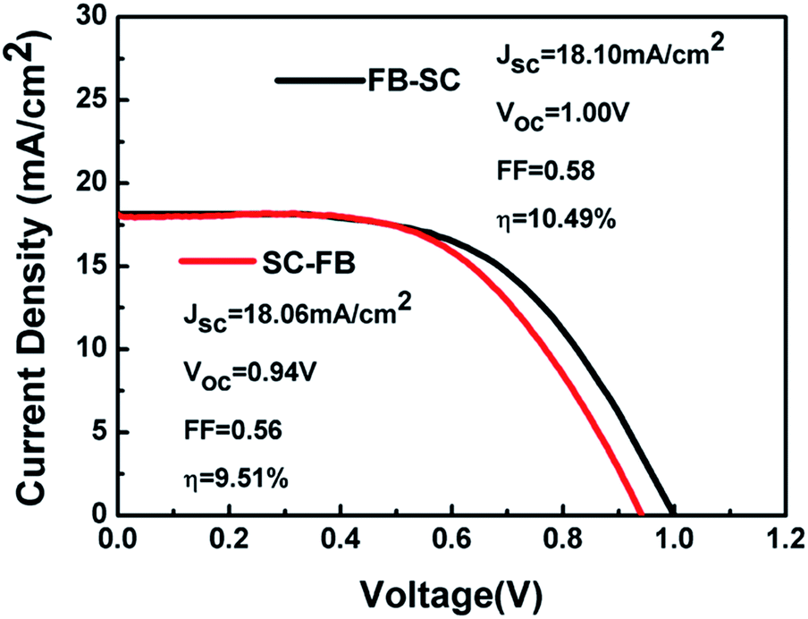 | ||
| Fig. 8 The FB–SC and SC–FB J–V curves for the best performing solar cell based on mp-graphene/SrTiO3 nanocomposites under simulated AM 1.5, 100 mW cm−2 solar irradiation. | ||
4. Conclusions
In conclusion, we succeeded in combining graphene with SrTiO3 as the anode material to fabricate organic–inorganic perovskite solar cells. Owing to the remarkably high charge mobility and electronic conductivity of graphene, an enhanced short-circuit current density was shown. The graphene content greatly affects the performance of the solar cell: excessive graphene decreased the light harvesting of the absorber layer, and introduced new recombination centers. By changing the amount of graphene to 20 mg, we have achieved a remarkable power conversion efficiency of 10% with a short-circuit current density of 18.08 mA cm−2 and open circuit voltage of 0.97 V, which is the best recorded efficiency for SrTiO3-based perovskite solar cells to date. Overall our research made up for the shortcoming of SrTiO3-based perovskite solar cells because of its low short-circuit current density compared with conventional TiO2-based perovskite solar cells, and maintenance of its relatively high open circuit voltage. However, the FF of our devices was still too low; we will undertake further studies to find out the cause.Acknowledgements
The authors gratefully acknowledge the financial support of the project from the National Science Foundation of China (no. 51202139, 51474142), Nature Science Foundation of Shanghai (no. 12ZR1443900), Specialized Research Fund for the Doctoral Program of Higher education (no. 20123108120022), the Program for Professor of Special Appointment (Eastern Scholar) at Shanghai Institutions of Higher Learning (2012) and the Key Projects in the National Science & Technology Pillar Program (2013BAE07B00).Notes and references
- C. V. Kumar, G. Sfyri, D. Raptis, E. Stathatos and P. Lianos, RSC Adv., 2015, 5, 3786 RSC.
- J. J. Choi, X. Yang, Z. M. Norman, S. J. L. Billinge and J. S. Owen, Nano Lett., 2014, 14, 127 CrossRef CAS PubMed.
- Y. Zhao, A. M. Nardes and K. Zhu, J. Phys. Chem. Lett., 2014, 5, 490 CrossRef CAS.
- N. G. Park, J. Phys. Chem. Lett., 2013, 4, 2423 CrossRef CAS.
- H. Zhou, Q. Chen, G. Li, S. Luo, T.-B. Song, H.-S. Duan, Z. Hong, J. You, Y. Liu and Y. Yang, Science, 2014, 345, 542 CrossRef CAS PubMed.
- Y. Bai, I. Mora-Sero, F. De Angelis, J. Bisquert and P. Wang, Chem. Rev., 2014, 114, 10095 CrossRef CAS PubMed.
- J.-W. Lee, T.-Y. Lee, P. J. Yoo, M. Grätzel, S. Mhaisalkar and N.-G. Park, J. Mater. Chem. A, 2014, 2, 9251–9259 CAS.
- L. Etgar, P. Gao, Z. Xue, Q. Peng, A. K. Chandiran, B. Liu, M. K. Nazeeruddin and M. Grätzel, J. Am. Chem. Soc., 2012, 134, 17396 CrossRef CAS PubMed.
- M. I. Dar, F. J. Ramos, Z. Xue, B. Liu, S. Ahmad, S. A. Shivashankar, M. K. Nazeeruddin and M. Grätzel, Chem. Mater., 2014, 26, 4675 CrossRef CAS.
- Y. Rong, Z. Ku, A. Mei, T. Liu, M. Xu, S. Ko, X. Li and H. Han, J. Phys. Chem. Lett., 2014, 5, 2160 CrossRef CAS.
- H. S. Kim, J. W. Lee, N. Yantara, P. P. Boix, S. A. Kulkarni, S. Mhaisalkar, M. Grätzel and N. G. Park, Nano Lett., 2013, 13, 2412 CrossRef CAS PubMed.
- K. Manseki, T. Ikeya, A. Tamura, T. Ban, T. Sugiura and T. Yoshida, RSC Adv., 2014, 4, 9652 RSC.
- J. Qiu, Y. Qiu, K. Yan, M. Zhong, C. Mu, H. Yan and S. Yang, Nanoscale, 2013, 5, 3245 RSC.
- H. Chen, Z. Wei, K. Yan, Y. Yi, J. Wang and S. Yang, Faraday Discuss., 2014, 176, 271 RSC.
- M. Yang, R. Guo, K. Kadel, Y. Liu, K. O’Shea, R. Bone, X. Wang, J. He and W. Li, J. Mater. Chem. A, 2014, 2, 19616 CAS.
- X. Gao, J. Li, J. Baker, Y. Hou, D. Guan, J. Chen and C. Yuan, Chem. Commun., 2014, 50, 6368 RSC.
- Y. M. Xiao, G. Y. Han, Y. P. Li, M. Y. Li and J. H. Wu, J. Mater. Chem. A, 2014, 2, 16856 CAS.
- S. Dharani, H. K. Mulmudi, N. Yantara, P. T. Thu Trang, N. G. Park, M. Gräetzel, S. Mhaisalkar, N. Mathews and P. P. Boix, Nanoscale, 2014, 6, 1675 RSC.
- Q. Jiang, X. Sheng, Y. Li, X. Feng and T. Xu, Chem. Commun., 2014, 50, 14720 RSC.
- Y. Yu, J. Li, D. Geng, J. Wang, L. Zhang, T. L. Andrew, M. S. Arnold and X. Wang, ACS Nano, 2015, 9, 564 CrossRef CAS PubMed.
- E. J. Crossland, N. Noel, V. Sivaram, T. Leijtens, J. A. Alexander-Webber and H. J. Snaith, Nature, 2013, 495, 215 CrossRef CAS PubMed.
- Q. Zhang, C. S. Dandeneau, X. Zhou and G. Cao, Adv. Mater., 2009, 21, 4087 CrossRef CAS PubMed.
- J. A. Anta, E. Guillén and R. Tena-Zaera, J. Phys. Chem. C, 2012, 116, 11413 CAS.
- D. Bi, G. Boschloo, S. Schwarzmuller, L. Yang, E. M. Johansson and A. Hagfeldt, Nanoscale, 2013, 5, 11686 RSC.
- D. Y. Son, J. H. Im, H. S. Kim and N. G. Park, J. Phys. Chem. C, 2014, 118, 16567 CAS.
- D. Liu and T. L. Kelly, Nat. Photonics, 2014, 8, 133–138 CrossRef CAS PubMed.
- M. M. Lee, J. Teuscher, T. Miyasaka, T. N. Murakami and H. J. Snaith, Science, 2012, 338, 643 CrossRef CAS PubMed.
- Y. H. Hu, Adv. Mater., 2014, 26, 2102 CrossRef CAS PubMed.
- E. Edri, S. Kirmayer, D. Cahen and G. Hodes, J. Phys. Chem. Lett., 2013, 4, 897 CrossRef CAS.
- D. Bi, S.-J. Moon, L. Häggman, G. Boschloo, L. Yang, E. M. J. Johansson, M. K. Nazeeruddin, M. Grätzel and A. Hagfeldt, RSC Adv., 2013, 3, 18762 RSC.
- H. S. Kim, I. Mora-Sero, V. Gonzalez-Pedro, F. Fabregat- Santiago, E. J. Juarez-Perez, N. G. Park and J. Bisquert, Nat. Commun., 2013, 4, 2242 Search PubMed.
- S. H. Hwang, J. Roh, J. Lee, J. Ryu, J. Yun and J. Jang, J. Mater. Chem. A, 2014, 2, 16429 CAS.
- K. Ueno, S. Nakamura, H. Shimotani, A. Ohtomo, N. Kimura, T. Nojima, H. Aoki, Y. Iwasa and M. Kawasaki, Nat. Mater., 2008, 7, 855 CrossRef CAS PubMed.
- M. Dawber, K. M. Rabe and J. F. Scott, Rev. Mod. Phys., 2005, 77, 1083 CrossRef CAS.
- H. Ohta, S. Kim, Y. Mune, T. Mizoguchi, K. Nomura, S. Ohta, T. Nomura, Y. Nakanishi, Y. Ikuhara, M. Hirano, H. Hosono and K. Koumoto, Nat. Mater., 2007, 6, 129 CrossRef CAS PubMed.
- O. N. Tufte and P. W. Chapman, Phys. Rev., 1967, 155, 796 CrossRef CAS.
- Q. Zhang, C. S. Dandeneau, X. Zhou and G. Cao, Adv. Mater., 2009, 21, 4087 CrossRef CAS PubMed.
- A. Bera, K. Wu, A. Sheikh, E. Alarousu, O. F. Mohammed and T. Wu, J. Phys. Chem. C, 2014, 118, 28494 CAS.
- J.-H. Chen, C. Jang, S. Xiao, M. Ishigami and M. S. Fuhrer, Nat. Nanotechnol., 2008, 3, 206 CrossRef CAS PubMed.
- A. K. Geim and K. S. Novoselov, Nat. Mater., 2007, 6, 183 CrossRef CAS PubMed.
- S. V. Morozov, K. S. Novoselov, M. I. Katsnelson, F. Schedin, D. C. Elias, J. A. Jaszczak and A. K. Geim, Phys. Rev. Lett., 2008, 100, 016602 CrossRef CAS.
- H. Mao, F. Hu, Q.-L. Ye, Y. Xu, X. Yang and B. Lu, Nanoscale, 2014, 6, 8149 RSC.
- L. Chen, Y. Zhou, W. Tu, Z. Li, C. Bao, H. Dai, T. Yu, J. Liu and Z. Zou, Nanoscale, 2013, 5, 3481 RSC.
- J. J. Wang, J. M. Ball, E. M. Barea, A. Abate, J. A. Alexander-Webber, J. Huang, M. Saliba, I. Mora-Sero, J. Bisquert, H. J. Snaith and R. J. Nicholas, Nano Lett., 2014, 14, 724 CrossRef CAS PubMed.
- S. R. Jang, K. Zhu, M. J. Ko, K. Kim, C. Kim, N. G. Park and A. J. Frank, ACS Nano, 2011, 5, 8267 CrossRef CAS PubMed.
- S. Ouyang, H. Tong, N. Umezawa, J. Cao, P. Li, Y. Bi, Y. Zhang and J. Ye, J. Am. Chem. Soc., 2012, 134, 1974 CrossRef CAS PubMed.
- J. Zhang, J. H. Bang, C. Tang and P. V. Kamat, ACS Nano, 2010, 4, 387 CrossRef CAS PubMed.
- N. J. Jeon, J. H. Noh, Y. C. Kim, W. S. Yang, S. Ryu and S. I. Seok, Nat. Mater., 2014, 13, 897 CrossRef CAS PubMed.
- J. T. Wang, J. M. Ball, E. M. Barea, A. Abate, J. A. Alexander-Webber, J. Huang, M. Saliba, I. Mora-Sero, J. Bisquert, H. J. Snaith and R. J. Nicholas, Nano Lett., 2014, 14, 724 CrossRef CAS PubMed.
| This journal is © The Royal Society of Chemistry 2015 |