Modification of a thin layer of α-Fe2O3 onto a largely voided TiO2 nanorod array as a photoanode to significantly improve the photoelectrochemical performance toward water oxidation

Lianwen Jia abc, Jiale Xieabc, Chunxian Guoabc and Chang Ming Li*abc
aInstitute for Clean Energy & Advanced Materials, Southwest University, Chongqing 400715, P. R. China. E-mail: ecmli@swu.edu.cn
bChongqing Key Laboratory for Advanced Materials & Technologies of Clean Electrical Power Sources, Chongqing 400715, P. R. China
cFaculty of Materials and Energy, Southwest University, Chongqing 400715, P. R. China

Received 12th May 2015 , Accepted 7th July 2015

First published on 7th July 2015


Abstract

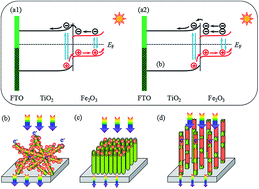
A largely voided TiO2 nanorod array was synthesized and further modified with a thin layer of α-Fe2O3 (Fe2O3@TiO2), by the pyrolysis of an FeCl3 ethanol solution, as a photoanode toward water oxidation, showing significantly improved photoelectrochemical performance over a TiO2 nanorod array. Among all of the Fe2O3 decorated TiO2-based photoanodes, the optimal voided Fe2O3@TiO2 nanorod array photoanode delivered the largest photocurrent density of 3.39 mA cm−2 at 1.23 V (vs. RHE) and the highest applied bias photon-to-current efficiency (ABPE) (1.153%) under 100 mW cm−2 UV-vis light illumination. In particular, the ABPE for the as-prepared photoanode was ∼3.3 times higher than that of the plain TiO2 nanorod array (0.35%), ∼11.3 times higher than that of the Fe2O3-modified randomly arranged TiO2 nanorods and ∼6.2 times higher than that of a Fe2O3-modified densely arranged TiO2 nanotube array. The significant enhancement mainly originates from the large voids in the nanorod array allowing a thin layer of Fe2O3 to fully modify the TiO2 nanorods, which improves the absorption of UV light, boosts the charge interface transfer rate, reduces the charge diffusion length and suppresses the charge recombination process. This work demonstrates a feasible route to improving the photoelectrochemical catalytic performance of TiO2 semiconductors toward water splitting.


1. Introduction

Photoelectrochemical (PEC) water splitting using solar energy to produce clean energy without a carbon footprint has attracted increasing attention. Since the seminal demonstration of PEC water splitting using n-type TiO2 by Honda and Fujishima in 1972,1 considerable efforts have been devoted to developing suitable photoanode materials with unique nanostructures for further improved water oxidation efficiency.2–9 Water oxidation is a slow kinetic process resulting from multi-electron transfers involving multi-protons. Therefore, developing an efficient PEC anode toward water oxidation is critical for the commercialization of PEC water splitting.

Among the various photoanodes, hydrothermally synthesized rutile TiO2 nanorods (NRs) have a large surface area, fast charge transport and a short diffusion distance for the photogenerated carriers.10 However, as a result of the wide band gap (3.0 eV) of rutile TiO2, it only absorbs light in the UV regions (less than 5% over the full solar energy), which significantly limits its efficiency. Therefore, TiO2 is often modified by various materials like metal ion/nonmetal ion dopants, and organic dyes or metal complexes for surface sensitization, surface fluorination and narrow band gap semiconductor coupling.11,12 Wu et al. have reported the direct formation of nanosized CdS-coupled TiO2 nanocrystals by a microemulsion-mediated solvothermal method.13 The formed heterojunction between CdS and TiO2 can provide efficient charge carrier separation and a more efficient matching of the solar spectra. Another semiconductor α-Fe2O3 (hematite) has been used as a photoanode material due to its favorable narrow optical band gap (2.0–2.2 eV), excellent chemical stability, natural abundance and low cost.14–19 The Fe2O3 in a TiO2/Fe2O3 heterojunction structure could enhance the light absorption due to its narrow bandgap while facilitating the transportation of the holes from the inside of the electrode to the semiconductor/electrolyte interface because of the more negative valence band level. Moreover, a TiO2/Fe2O3 heterojunction can efficiently enhance the charge separation.20 Luan et al. fabricated randomly arranged TiO2 nanorods (RNRs) coupled with Fe2O3 toward water oxidation,20 they showed an improved PEC performance over TiO2 alone but a poor photocurrent density of ∼0.3 mA cm−2 at 1.23 V (vs. RHE),20 which is even lower than the reported typical performance for the Fe2O3/TiO2 photoanode and is very likely to be ascribed to a high charge transfer resistance and a high charge recombination at more boundaries of the randomly arranged TiO2 nanorods. Mao et al. synthesized α-Fe2O3 nanoparticles decorated with a densely arranged TiO2 nanotube array through an electrochemical deposition method, which improved the photocurrent density (∼0.55 mA cm−2 at 1.23 V vs. RHE)21 but was still not as good as the reported TiO2-based photoanode possibly due to the densely packed tube array only allowing Fe2O3 deposition on the top surface to result in a very limited effect.22 Cao et al. fabricated a Fe2O3@TiO2 heterostructure nanorod array via chemical bath deposition to improve the PEC activity of TiO2. The heterojunction yielded a very low photocurrent density of 39.75 μA cm−2 at a bias potential of 0 V (vs. Ag/AgCl),23 possibly due to the thick coating of Fe2O3 resulting in a high charge transport resistivity. Zhao et al. synthesized TiO2 NR/Fe2O3 nanoparticle core–shell nanostructures for PEC water splitting through a chemical bath deposition method,24 they exhibited an improved photocurrent density of ∼2.5 mA cm−2 at 1.23 V (vs. RHE), which is mainly contributed from the enhanced visible light absorbance by the large amount of Fe2O3 modification. Due to poor conductivity and a short hole diffusion distance (2–4 nm),18 a thin layer of TiO2 was used as an interlayer to facilitate the electron transfer in the Fe2O3 photoanode.25–27 Although the various approaches discussed above have been used to improve the photoelectrochemical catalytic activity of the TiO2 based-photoanodes, the conversion efficiency and the oxygen evolution current density are still relatively low. In addition, the enhancement mechanisms of the Fe2O3 modification for the TiO2 based-photoanodes with different nanostructures have not been systematically investigated.

To significantly improve the performance of the Fe2O3 nanoparticle-decorated TiO2 based photoanodes, herein we fabricate a one-dimensional largely voided TiO2 nanorod array and allow a thin layer of Fe2O3 to fully modify the nanorods as a photoanode toward water oxidation, which delivers the highest photocurrent density (3.39 mA cm−2 at 1.23 V vs. RHE) under 100 mW cm−2 UV-vis light illumination and also the highest applied bias photon-to-current efficiency (ABPE) (1.15%) among all the reported works. In particular, the ABPE for the as-prepared photoanode is ∼3.3 times higher than that of the plain TiO2 nanorod array (0.35%), ∼11.3 times higher than that of the Fe2O3-modified randomly arranged TiO2 nanorods and ∼6.2 times higher than that of the Fe2O3-modified densely arranged TiO2 nanotube array. The enhancement mechanism is further investigated and proposed for scientific insight.

2. Experimental method

2.1 Preparation of the TiO2 nanorod array

To synthesise the TiO2 nanorod array on FTO glasses, 6 ml of concentrated hydrochloric acid (HCl, 36–38% by weight) was firstly diluted into 13 ml of deionized (DI) water. Then 0.2 ml of titanium(IV) isopropoxide (TTIP) was added into the above solution and was stirred for 5 min. The mixture solution was transferred into a 25 ml Teflon-lined stainless steel autoclave. FTO glasses were put into the autoclave with the conductive side facing down. The hydrothermal synthesis was kept at 180 °C for 3 h. After the hydrothermal reaction, the autoclave was cooled to room temperature and the FTO substrates were taken out, rinsed adequately with DI water and allowed to dry in air. The obtained samples were then calcined in a muffle furnace at 450 °C for 60 min in air.

2.2 Preparation of the Fe2O3@TiO2 nanorod array

To synthesise the Fe2O3@TiO2 nanorod array, a series of ethanol solutions with different FeCl3 concentrations from 0.5 to 10 mM were prepared by dissolving FeCl3·6H2O in ethanol. An ethanol based FeCl3 solution (10 μl) was drop-deposited onto the as-prepared TiO2 nanorods and dried in air for 1 min. Then the FTO substrates were heated on a hotplate in air at 500 °C for 20 min. The Fe2O3 layer was formed as the shell of the Fe2O3@TiO2 nanorod array structure. The conversion of FeCl3 to Fe2O3 could follow equations such as:
 
FeCl3 + 3H2O → Fe(OH)3 + 3HCl (1)
 
2Fe(OH)3 = Fe2O3 + 3H2O (2)

The thickness of the Fe2O3 layer was tuned by the FeCl3 solution concentration and an optimal thickness of ∼100 nm was obtained.

2.3 Material characterization

The morphology and structure of the synthesized electrode materials were investigated using a field emission scanning electron microscope (FESEM, JSM-7800F) and transmission electron microscopy (TEM, JEM-2100). The composition of the Fe2O3@TiO2 nanorod array electrodes was determined by energy dispersive X-ray spectroscopy (EDS). The crystal structure was characterized by powder X-ray diffraction (XRD, XRD-7000) and X-ray photoelectron spectroscopy (XPS, ESCALAB 250). The optical properties were tested with a UV-2550 spectrophotometer (Shimadzu Co.).

2.4 Photoelectrochemical measurements

The photoelectrochemical water splitting device was constructed with a three-electrode system comprising a photoanode (0.5 cm2) as the working electrode, platinum foil (2.5 cm2) as the counter electrode and a saturated calomel electrode (SCE) as the reference electrode. A 1 M NaOH aqueous solution was used as the electrolyte. The light source was a 300 W Xe lamp and the illumination intensity near the photoelectrode surface was 100 mW cm−2. Linear-sweep voltammetry (LSV) was performed with an electrochemical workstation (CHI Instruments, CHI660D). The photocurrent from H2O2 (JH2O2) oxidation was measured in a 1 M NaOH–0.5 M H2O2 solution. The incident photon to current conversion efficiency (IPCE) was measured in a two-electrode system without external bias. The IPCE is calculated using eqn (3)
 
IPCE = (1240I)/(λJlight) (3)
where I is the photocurrent density, λ is the incident light wavelength and Jlight is the measured irradiance. All the measurements were carried out in air at room temperature.

3. Results and discussion

3.1 Properties of the Fe2O3@TiO2 nanorod array photoanode

The crystal structure and composition of the Fe2O3@TiO2 nanorod array electrode were examined by X-ray diffraction (XRD) and energy dispersive X-ray spectroscopy (EDS), respectively. Fig. 1a shows that all of the XRD diffraction peaks could be indexed to the rutile TiO2 (JCPDS card no. 21-1276) and the rhombohedral phase of α-Fe2O3 (JCPDS card no. 33-664). For the TiO2 NRs, only the (101), (002), and (112) diffraction peaks were observed. Due to the small amount of Fe2O3, the peak intensity of Fe2O3 is not obvious but some small peaks belonging to α-Fe2O3 can be identified. All of these peaks are marked with a plum blossom shape in Fig. 1a. At the same time, we performed EDS analysis to determine the kinds of elements in the Fe2O3@TiO2 nanorod array (Fig. 1b). Titanium, oxygen and iron elements were found. The optimal molar ratio of Fe2O3/TiO2 was about 2.6%, indicating a relative low loading of Fe2O3.
image file: c5ra08885b-f1.tif
Fig. 1 Classic crystal, composition and optical characterizations. (a) XRD patterns of the TiO2 nanorod array and the Fe2O3@TiO2 nanorod array. (b) EDS analysis of the Fe2O3@TiO2 nanorod array. (c) UV-vis diffuse reflectance spectra of the bare and Fe2O3 modified TiO2 nanorod arrays.

The optical absorption property of a photoelectrode is very critical for the photogeneration of electron–hole pairs. We performed UV-vis diffuse reflectance spectroscopy of the bare and Fe2O3 modified TiO2 nanorod arrays.As shown in Fig. 1c, the absorption spectra exhibit a slight blue-shift, which is very different to the spectra resulting from a large amount of Fe2O3 modification, as reported.20 However, the small amount of Fe2O3 modification can greatly enhance the UV light absorption.28 This phenomenon was further confirmed by external quantum efficiency measurements later on. This mainly comes from the low absorption coefficient of Fe2O3, resulting in the low visible light absorption from a thin layer of Fe2O3.29 Moreover, the incomplete covering from the Fe2O3 thin layer is another reason.

The morphology and structural characteristics of the electrodes were examined by field emission scanning electron microscopy (FESEM) and transmission electron microscopy (TEM). Fig. 2a and b show the FESEM images of the TiO2 nanorod array. The nanorods with diameters in a range of 50 to 250 nm and a mean length of 4.1 μm form an orderly arranged array but possess plenty of voids (∼200–1000 nm) to separate the rods from each other (Fig. 2 and inset of Fig. 2d). The voids are significantly larger than those of the used TiO2 nanotube arrays (0–50 nm).21 The cross section of the TiO2 nanorods shows a tetragonal shape, indicating the rutile crystal structure of TiO2. This is in good agreement with the XRD results. Fig. 2c and d show the FESEM images of the Fe2O3@TiO2 nanorod array, from which the largely voided TiO2 nanorod array structure can be seen (the inset of Fig. 2d) and, thanks to the large voids among the nanorods, the thin layer of Fe2O3 can fully cover the TiO2 nanorods which can be clearly observed in Fig. 2c–e. As shown in the HRTEM images (Fig. 2e1–e3), the lattice fringes with interplanar spacing of rutile TiO2 (d110 = 3.2 Å) and α-Fe2O3 (d110 = 2.5 Å and d104 = 2.7 Å) can be observed in Fig. 2e.


image file: c5ra08885b-f2.tif
Fig. 2 Morphology characterization by SEM and TEM. (a and b) Top-view SEM images of the TiO2 nanorod array. (c and d) Top-view and section-view SEM images of the Fe2O3@TiO2 nanorod array. The thin layer of Fe2O3 is marked out with arrows. The inset is the low magnification SEM image. (e–e3) TEM images of the Fe2O3@TiO2 nanorod array.

X-ray photoelectron spectroscopy (XPS) was employed to investigate the existence of the elements and defects as shown in Fig. 3. The binding energies for Ti 2p3/2 and 2p1/2 were observed at 458.3 and 464.0 eV, which are typical for the XPS spectra of Ti4+ in TiO2.30 Moreover, no trace of Ti3+ or Ti2+, with the Ti 2p3/2 located at 457.6 eV and 456.4 eV respectively, was observed. The O 1s spectrum (Fig. 3c) was well fitted by four Gaussian components at 529.2, 529.6, 530.5 and 531.7 eV. The binding energy at 529.2 eV can be assigned to oxygen bound to the Ti4+ ions in TiO2, while the binding energy located at 529.6 eV can be attributed to Fe–O bound oxygen. The shoulder at 530.5 eV implies that the surface is partially covered with hydroxide OH groups or C–O bound oxygen. This also implies that there are some local oxygen vacancies, which can introduce the defect levels and induce the charge recombination. The binding energy at 531.7 eV comes from absorbed O2. The XPS spectrum of Fe 2p (Fig. 3b) shows three dominant peaks including Fe 2p3/2 at 710.9 eV, Fe 2p1/2 at 725.0 eV and a satellite peak at 717.9 eV, which is evidence for the presence of α-Fe2O3.31 The XPS results and analysis clearly show the successful modification of Fe2O3 on the TiO2 nanorod array and the surface chemistry.


image file: c5ra08885b-f3.tif
Fig. 3 XPS surface analysis of the Fe2O3@TiO2 nanorod array. (a) Ti 2p XPS spectrum. (b) Fe 2p XPS spectrum. (c) O 1s XPS spectrum.

3.2 Photoelectrochemical behaviors of the Fe2O3@TiO2 nanorod array photoanode

PEC water splitting performance was evaluated using a three-electrode cell comprising a Fe2O3@TiO2 nanorod array photoanode, a Pt counter electrode and a saturated calomel (SCE) reference electrode in a 1.0 M NaOH aqueous solution. 100 mW cm−2 UV-vis light illumination was used from the front. The efficient illuminated area of the working electrode is around 0.5 cm2.

Linear sweep voltammetry (LSV) is a common electrochemical technique to investigate the charge-carrier characteristics at a semiconductor/electrolyte interface. The measured LSV plots of the different photoanodes are shown in Fig. 4a. The photocurrent density and the onset potential are plotted versus the concentration of the FeCl3 solution as in Fig. 4b. When a 1.5 mM FeCl3 ethanol solution is used, the Fe2O3@TiO2 nanorod array electrode achieves the highest photocurrent density of 3.39 mA cm−2 at 1.23 V (vs. RHE) while possessing the most negative onset potential of 0.34 V (vs. RHE). In contrast, a large amount of Fe2O3 loading on the TiO2 nanorods gives the lowest photocurrent density of 0.32 mA cm−2 and the most positive onset potential of 0.53 V. It is known that a more negative onset potential has a higher electrocatalytic activity towards an electrooxidation while a higher current density at the same polarization potential indicates a faster electrode reaction rate resulting from faster electrode kinetics or/and a higher charge transfer rate. Thus, the results indicate that the Fe2O3@TiO2 nanorod array photoanode has a higher photoelectrocatalytic activity and a better charge transfer/transport rate than that of the Fe2O3@TiO2 RNRs one, which is very likely to have the former’s better conductivity and shorter hole transport distance if in an arrayed structure with a faster interfacial charge transfer rate.32


image file: c5ra08885b-f4.tif
Fig. 4 Photoelectrochemical performance measurements. (a) LSV curves of the Fe2O3@TiO2 nanorod array with different amounts of Fe2O3. (b) The onset potential and photocurrent density at 1.23 V (vs. RHE) under AM 1.5 irradiation. (c) The ABPE efficiency calculated from the photocurrent vs. potential plots. (d) The transient current density of various Fe2O3@TiO2 nanorod array electrodes modified with different concentrations of Fe2O3 under chopped light illumination at 0.6 V (vs. SCE).

The applied bias photon-to-current efficiency (ABPE) can be calculated to evaluate the photoanode efficiency quantitatively in terms of the following formula:

 
η (%) = J (1.23 − V)/P × 100 (4)
where J is the current density under visible light irradiation, V is the applied voltage versus RHE, and P is the input light power intensity of 100 mW cm−2. The calculated ABPE efficiencies are plotted as a function of the applied bias in Fig. 4c. The Fe2O3@TiO2 nanorod array electrode modified with the 1.5 mM FeCl3 solution shows a maximal conversion efficiency of 1.15% at 0.7 V (vs. RHE), which is ∼3.3 times higher than that of the bare TiO2 nanorod array electrode (0.35%) and ∼11.3 times higher than the reported Fe2O3@TiO2 RNRs electrode20 and ∼6.2 times higher than the densely arranged TiO2 nanotube array.21 Fig. 4d illustrates the transient current density of the various Fe2O3@TiO2 nanorod array electrodes modified with different concentrations of Fe2O3 under chopped light illumination at a 0.6 V (vs. SCE) external bias. These results confirm the observed trends in Fig. 4a. Moreover, all the electrodes show good photoresponses. Nevertheless, one can find that the photocurrent increases with the increasing of the light illumination. This should originate from a type I (straddling bandgap) TiO2/Fe2O3 heterojunction.33 The excited electrons are accumulated on the conduction band of Fe2O3 at the initial illumination, inducing a low photocurrent at the beginning. After enough electron accumulation, the electrons can favorably transfer from Fe2O3 to TiO2, delivering a stable photocurrent. The mechanism detail will be discussed later.

To further understand the role of Fe2O3 in the charge transport process, the electrochemical impedance spectroscopy (EIS) spectra were determined at an open circuit potential and a frequency range from 100 kHz to 1 Hz under illumination (Fig. 5a and b). Two semicircles can be distinguished from the Nyquist plots of the TiO2 nanorod array and Fe2O3@TiO2 nanorod array electrodes. The high-frequency semicircle can be ascribed to the charge-transfer process in the semiconductor depletion layer while the low-frequency arc results from the electron transfer in the Helmholtz layer. The experimental data was fitted with the equivalent circuit (inset of Fig. 5a). A good agreement between the measured and fitted data indicates that the proposed equivalent circuit could accurately describe the main charge transfer processes. The fitting parameters are shown in Table 1, where Rs is the series resistance of the cell. R1 of the CPE1 with a high frequency response corresponds to the charge transport in the depletion layer. The impedance response at low to intermediate frequencies (R2, CPE2) is accordingly designated to events occurring in the Helmholtz layer. Compared with the plain TiO2 nanorod array electrode, the Fe2O3@TiO2 nanorod array electrode has smaller R1 and R2 values, thus clearly indicating an enhancement of the charge transfer in the depletion layer and the Helmholtz layer. The higher capacitance of the CPE1 and the CPE2 corresponds to the presence of more charge being separated effectively at the interface, thus indicating a reduction in the charge recombination possibility in the Fe2O3@TiO2 nanorod array electrode.


image file: c5ra08885b-f5.tif
Fig. 5 AC impedance and IPCE measurements. (a and b) Nyquist plots of the Fe2O3@TiO2 nanorod array with different amounts of Fe2O3 under AM 1.5 irradiation. (c) Bode plots of the bare TiO2 and Fe2O3@TiO2 nanorod array with 1.5 mM FeCl3. (d) The IPCE efficiency of the Fe2O3@TiO2 nanorod array, no external bias is applied.
Table 1 Calculated electronic parameters from Nyquist plots
Electrode Rs (Ω) CPE1 (×10−6, F) R1 (Ω) CPE2 (×10−5, F) R2 (Ω)
TiO2 nanorod array 3.28 4.25 136.40 2.10 1247.00
Fe2O3@TiO2 nanorod array 2.03 10.04 88.40 19.00 105.10


As shown in Fig. 5c, the characteristic maximum frequency peaks (fmax) decrease obviously after Fe2O3 modification. Theoretically, there is no current passing through the whole circuit at an open circuit potential and all the electrons injected into the conduction band must come from the PEC reaction at the electrode/electrolyte interface.34 The lifetime of the electrons for recombination with a time constant (τn) is correlated with fmax as in eqn (5).35

 
τn = 1/(2πfmax) (5)

The τn values calculated from the Bode plots are 1.93 and 8.96 ms for the TiO2 nanorod array and Fe2O3@TiO2 nanorod array electrodes, respectively. The larger τn means less charge recombination. This result reveals that Fe2O3 modification can efficiently suppress the charge recombination for a higher PEC current.

IPCE is often used to explore the fundamental insight of the PEC process. The IPCE was measured without any applied external bias as shown in Fig. 5d. Most of the Fe2O3 modified electrodes show a larger integrated photocurrent value than the bare TiO2 nanorod array electrode. This is in good agreement with the result of the improved photocurrent densities after Fe2O3 modification. The maximum IPCE value for the TiO2 nanorod array is 18.52% at 395 nm, while the optimal Fe2O3@TiO2 nanorod array electrode has a maximum IPCE of 52.53% at 375 nm. This clearly suggests that Fe2O3 modification can efficiently suppress the charge recombination while improving the charge separation, possibly mainly due to the enhanced light absorption strength from the Fe2O3 modification for strong charge separation. It is worthy of a note that the light absorption of Fe2O3 is proportional to its amount while the charge recombination could be increased, and thus an optimal thickness exists. The significantly improved UV absorption is also in good agreement with the results of the UV-vis diffuse reflectance spectroscopy.

To gain more physical insight into the role of Fe2O3 modification, the charge injection efficiencies of the TiO2 nanorod array and Fe2O3@TiO2 nanorod array electrodes were examined by comparing the photocurrent from water (JH2O) and H2O2 (JH2O2) oxidation. As we know, H2O2 as a hole scavenger can be used to assess the performance of surface hole injection.36 The charge injection efficiency (P) can be calculated from:

 
P = JH2O/JH2O2 × 100% (6)

The calculated results are illustrated in Fig. 6a. The charge injection efficiency of the TiO2 electrode is lower at high potential, indicating that the holes are accumulated on the surface of the electrode. Once coupled with Fe2O3, the charge injection efficiency of the Fe2O3@TiO2 nanorod array electrode almost remains high efficiency (∼85%) from low to high potential, indicating that Fe2O3 significantly promotes the hole injection on the surface of the TiO2 photoanode. This is in accordance with the reported results20 and is further confirmed by the Mott–Schottky (MS) plots in Fig. 6b, in which the slope has an inverse relationship with the electron density of n-type semiconductor films35 and the Fe2O3@TiO2 nanorod array electrode shifts the conduction band edge to a more negative value, showing that Fe2O3 modification offers better kinetics of water oxidation.37


image file: c5ra08885b-f6.tif
Fig. 6 (a) Charge injection efficiency of the bare TiO2 and Fe2O3@TiO2 nanorod array electrodes under AM 1.5 irradiation. (b) Mott–Schottky plots of the bare TiO2 and Fe2O3@TiO2 nanorod array electrodes in the dark at a frequency of 1000 Hz.

3.3 Photoelectrocatalytic enhancement mechanism of the Fe2O3@TiO2 nanorod array

Fig. 7 schematically illustrates the nanostructure of the Fe2O3@TiO2 nanorod array photoanode with comparison to the Fe2O3@TiO2 RNRs one and the densely arranged Fe2O3@TiO2 nanotube array, and the charge separation/transport mechanism. In terms of the energy band structure, the straddling bandgap heterojunction forms after the Fe2O3 and TiO2 contact as shown in Fig. 7a1. The band bending can enhance the continuity of the valence bands, which makes it easier for the holes to separate from TiO2 to Fe2O3, and then enhance the charge injection. The electrons photogenerated on the Fe2O3 layer can be accumulated on the conduction band of Fe2O3, and partially transferred to TiO2 when the electrons are excited with high-energy light.20 That is to say, under high-energy light excitation (<550 nm),20 the electrons can be excited to lower conduction band levels then to the conduction band edges of Fe2O3 and TiO2. These electrons would thermodynamically transfer to the conduction band of TiO2. After a period of time, more electrons accumulated on the low conduction band levels of Fe2O3 and this made it easier for the electrons to transfer to the conduction band of TiO2 (Fig. 7a2).38 Fig. 7b–d show that the enhancement can be mainly attributed to the thin layer modification of Fe2O3 on the largely voided TiO2 nanorod array structure. The nanorod array structure with such a thin layer of modification can absorb more UV light than the random arranged nanorods to excite more electron–hole pairs, which is supported by reported work.39 The nanoarray as an “electron expressway” also can facilitate the charge transport and shorten the charge diffusion length, while the random nanorods will introduce a number of boundary resistances. Further, although Fe2O3 possesses a narrow energy gap to enhance the charge injection at the electrode/electrolyte interface, it has a long hole diffusion length (2–4 nm) as discussed above. Thus, a rational thin layer modification becomes critical for the efficient charge injection. In our work, a thin layer of Fe2O3 fully modified on the TiO2 nanorod array surface due to the voids in the structure can improve the absorption of UV light, boost the charge interface transfer rate, reduce the charge diffusion length and suppress the charge recombination process. This can also explain why a large amount of Fe2O3 incorporation into TiO2 nanorods can enhance UV-vis absorbance but leads to a decreased PEC performance rather than an improvement due to the long hole diffusion length.14,17 In comparison to the densely arranged Fe2O3/TiO2 nanotube array,21 the as-prepared largely voided TiO2 nanorods in this work not only allow a thin layer of Fe2O3 to fully cover the TiO2 nanorods instead of accumulating on the top of the TiO2 nanotubes but also greatly enhance the light absorption and electrolyte diffusion between the nanorods. In contrast, in the densely arranged Fe2O3/TiO2 nanotube array anode, due to the densely packed TiO2 nanotubes (40–90 nm) the Fe2O3 nanoparticles cannot go inside or/and outside of the nanotubes for modification but only deposit on the top surface of the nanotube array,22 of which the same phenomenon has also been reported. This not only clogs the pores but also inhibits the utilization of most parts of the nanotube array as the results indicate in ref. 22. This is why the photocurrent and ABPE of largely voided TiO2 nanorods is significantly higher than that of the Fe2O3 modified TiO2 nanotube array.
image file: c5ra08885b-f7.tif
Fig. 7 (a1 and a2) Schematic of the separation and transport of the charge carriers under UV-visible light irradiation between Fe2O3 and TiO2. (a1) Initial state. (a2) Stable state. (b) Schematic of the random TiO2 nanorods decorated with Fe2O3. (c) Schematic of the densely arranged TiO2 nanotube array decorated with Fe2O3. (d) Schematic of the largely voided TiO2 nanorod array modified with a thin layer of Fe2O3.

4. Conclusions

We successfully fabricated a one-dimensional largely voided TiO2 nanorod array followed by modification with a thin layer of Fe2O3 by pyrolysis. Under 100 mW cm−2 UV-vis light illumination, the ABPE efficiency of the TiO2 nanorod array electrode modified with Fe2O3 is greatly improved to 1.153%, which is ∼3.3 times higher than that of the bare TiO2 nanorod array (0.349%), ∼11.3 times higher than that of the Fe2O3-modified randomly arranged TiO2 nanorods and ∼6.2 times higher than that of the Fe2O3-modified densely arranged TiO2 nanotube array. The enhanced mechanism for the PEC water oxidation is systematically investigated and it is revealed that the improvement is mainly originated from a thin layer of Fe2O3 modification on the largely voided TiO2 nanorod array, which improves the absorption of UV light, boosts the charge interface transfer rate, reduces the charge diffusion length and suppresses the charge recombination process.

Acknowledgements

This work was supported by the Institute for Clean Energy & Advanced Materials (Southwest University, Chongqing, China), the Chongqing Key Laboratory for Advanced Materials and Technologies of Clean Energies (Chongqing, China), Chongqing Science and Technology Commission under cstc2012gjhz90002 (Chongqing, China), and the Chongqing development and reform commission and the National Natural Scientific Fund (No. 21375108).

Notes and references

  1. A. Fujishima and K. Honda, Nature, 1972, 238, 37–38 CrossRef CAS PubMed.
  2. S. M. A. Shibli, P. S. Arun and A. V. Raj, RSC Adv., 2015, 5, 19393–19399 RSC.
  3. A. N. Pinheiro, E. G. S. Firmiano, A. C. Rabelo, C. J. Dalmaschio and E. R. Leite, RSC Adv., 2014, 4, 2029–2036 RSC.
  4. H. Pan, S. Zhu, X. Lou, L. Mao, J. Lin, F. Tian and D. Zhang, RSC Adv., 2015, 5, 6543–6552 RSC.
  5. N. Naseri, P. Sangpour and S. H. Mousavi, RSC Adv., 2014, 4, 46697–46703 RSC.
  6. W.-H. Hung, T.-M. Chien, A.-Y. Lo, C.-M. Tseng and D. Li, RSC Adv., 2014, 4, 45710–45714 RSC.
  7. F.-X. Xiao, J. Miao, H. B. Tao, S.-F. Hung, H.-Y. Wang, H. B. Yang, J. Chen, R. Chen and B. Liu, Small, 2015, 11, 2115–2131 CrossRef CAS PubMed.
  8. B. Liu and E. S. Aydil, J. Am. Chem. Soc., 2009, 131, 3985–3990 CrossRef CAS PubMed.
  9. H. B. Yang, J. Miao, S.-F. Hung, F. Huo, H. M. Chen and B. Liu, ACS Nano, 2014, 8, 10403–10413 CrossRef CAS PubMed.
  10. A. I. Hochbaum and P. Yang, Chem. Rev., 2010, 110, 527–546 CrossRef CAS PubMed.
  11. C. S. Karthikeyan, H. Wietasch and M. Thelakkat, Adv. Mater., 2007, 19, 1091–1095 CrossRef CAS PubMed.
  12. M.-C. Wu, J. Hiltunen, A. Sápi, A. Avila, W. Larsson, H.-C. Liao, M. Huuhtanen, G. Tóth, A. Shchukarev and N. Laufer, ACS Nano, 2011, 5, 5025–5030 CrossRef CAS PubMed.
  13. L. Wu, J. C. Yu and X. Fu, J. Mol. Catal. A: Chem., 2006, 244, 25–32 CrossRef CAS PubMed.
  14. Y. Lin, G. Yuan, S. Sheehan, S. Zhou and D. Wang, Energy Environ. Sci., 2011, 4, 4862–4869 CAS.
  15. T. Hisatomi, F. Le Formal, M. Cornuz, J. Brillet, N. Tetreault, K. Sivula and M. Gratzel, Energy Environ. Sci., 2011, 4, 2512–2515 CAS.
  16. D. Cao, W. Luo, J. Feng, X. Zhao, Z. Li and Z. Zou, Energy Environ. Sci., 2014, 7, 752–759 CAS.
  17. K. Sivula, F. Le Formal and M. Grätzel, ChemSusChem, 2011, 4, 432–449 CrossRef CAS PubMed.
  18. Y.-S. Hu, A. Kleiman-Shwarsctein, A. J. Forman, D. Hazen, J.-N. Park and E. W. McFarland, Chem. Mater., 2008, 20, 3803–3805 CrossRef CAS.
  19. S. Chatman, P. Zarzycki and K. M. Rosso, ACS Appl. Mater. Interfaces, 2015, 7, 1550–1559 CAS.
  20. P. Luan, M. Xie, D. Liu, X. Fu and L. Jing, Sci. Rep., 2014, 4, 06180 CrossRef CAS PubMed.
  21. A. Mao, X. Meng, M. S. Kim, J.-B. Yu, G. Y. Han and J. H. Park, J. Nanosci. Nanotechnol., 2011, 11, 7290–7293 CrossRef CAS PubMed.
  22. J. A. Seabold, K. Shankar, R. H. Wilke, M. Paulose, O. K. Varghese, C. A. Grimes and K.-S. Choi, Chem. Mater., 2008, 20, 5266–5273 CrossRef CAS.
  23. C. Cao, C. Hu, W. Shen, S. Wang, S. Song and M. Wang, Mater. Res. Bull., 2015, 70, 155–162 CrossRef CAS PubMed.
  24. H. Zhao, W. Fu, H. Yang, Y. Xu, W. Zhao, Y. Zhang, H. Chen, Q. Jing, X. Qi, J. Cao, X. Zhou and Y. Li, Appl. Surf. Sci., 2011, 257, 8778–8783 CrossRef CAS PubMed.
  25. E. Noh, K. J. Noh, K. S. Yun, B. R. Kim, H. J. Jeong, H. J. Oh, S. C. Jung, W. S. Kang and S. J. Kim, Sci. World J., 2013, 723201,  DOI:10.1155/2013/723201.
  26. B.-R. Kim, H.-J. Oh, K.-S. Yun, S.-C. Jung, W. Kang and S.-J. Kim, Prog. Org. Coat., 2013, 76, 1869–1873 CrossRef CAS PubMed.
  27. H. J. Oh, K. J. Noh, B. R. Kim, W. Kang, S. C. Jung and S. J. Kim, Jpn. J. Appl. Phys., 2013, 52, 01AC15 CrossRef.
  28. Gurudayal, P. M. Chee, P. P. Boix, H. Ge, F. Yanan, J. Barber and L. H. Wong, ACS Appl. Mater. Interfaces, 2015, 7, 6852–6859 CAS.
  29. M. G. Walter, E. L. Warren, J. R. McKone, S. W. Boettcher, Q. X. Mi, E. A. Santori and N. S. Lewis, Chem. Rev., 2010, 110, 6446–6473 CrossRef CAS PubMed.
  30. D. W. Chu, A. Younis and S. A. Li, J. Phys. D: Appl. Phys., 2012, 45, 355306 CrossRef.
  31. T. Yamashita and P. Hayes, Appl. Surf. Sci., 2008, 254, 2441–2449 CrossRef CAS PubMed.
  32. J. L. Xie, C. X. Guo and C. M. Li, Energy Environ. Sci., 2014, 7, 2559–2579 CAS.
  33. H. Zhou, Y. Qu, T. Zeid and X. Duan, Energy Environ. Sci., 2012, 5, 6732–6743 CAS.
  34. M. Zhou, J. Bao, Y. Xu, J. Zhang, J. Xie, M. Guan, C. Wang, L. Wen, Y. Lei and Y. Xie, ACS Nano, 2014, 8, 7088–7098 CrossRef CAS PubMed.
  35. X. Wang, J. Xie and C. M. Li, J. Mater. Chem. A, 2015, 3, 1235–1242 CAS.
  36. D. K. Zhong, S. Choi and D. R. Gamelin, J. Am. Chem. Soc., 2011, 133, 18370–18377 CrossRef CAS PubMed.
  37. J. Z. Bloh, R. Dillert and D. W. Bahnemann, Phys. Chem. Chem. Phys., 2014, 16, 5833–5845 RSC.
  38. L. Peng, T. Xie, Y. Lu, H. Fan and D. Wang, Phys. Chem. Chem. Phys., 2010, 12, 8033–8041 RSC.
  39. B.-X. Lei, J.-Y. Liao, R. Zhang, J. Wang, C.-Y. Su and D.-B. Kuang, J. Phys. Chem. C, 2010, 114, 15228–15233 CAS.

Footnotes

Electronic supplementary information (ESI) available. See DOI: 10.1039/c5ra08885b
Equal contributors.

This journal is © The Royal Society of Chemistry 2015
Click here to see how this site uses Cookies. View our privacy policy here.