Soon Moon Jeong*a,
Jung-Hye Kima,
Seongkyu Songa,
Jungpil Seob,
Jung-Il Hongb,
Na Young Hac,
Hideo Takezoede,
Jaewook Jeong‡
a and
Hyunmin Kima
aDivision of Nano and Energy Convergence Research, DGIST, Daegu 711-873, Republic of Korea. E-mail: smjeong@dgist.ac.kr
bDepartment of Emerging Materials Science, DGIST, Daegu 711-873, Republic of Korea
cDepartment of Physics and Department of Energy System Research, Ajou University, Suwon 443-749, Republic of Korea
dDepartment of Organic and Polymeric Materials, Tokyo Institute of Technology, Tokyo 152-8552, Japan
eToyota Physical and Chemical Research Institute, 41-1, Yokomichi, Nagakute, Aichi 480-1192, Japan
First published on 2nd June 2015
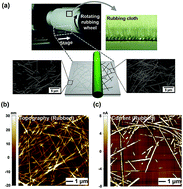
This paper explores the use of rubbing for alleviating the problem of lost electrical conductivity, which is typically caused by the use of nonconductive polymers, to improve the substrate adhesion and surface roughness of metal nanowire networks. This process is used to create composite transparent electrodes based on a network of silver nanowires (AgNWs) fully-embedded in PVA, which, after mechanical rubbing, exhibit both a smoother surface and superior electromechanical stability.
With all TCEs, there are several critical issues that need to be solved to ensure large-scale production, such as adhesion to a substrate and surface roughness. This poses a problem with networks of bare AgNWs coated onto a substrate, as these are typically both highly coarse and poorly adhered, and therefore easily removed by external friction. This has led to the development of several different approaches, such as burying AgNWs into the surface of polymer matrix,11 or over coating additional layers of conducting polymer12 (PEDOT:PSS) or metal oxide nanoparticles (NPs).13 In the case of the former, the choice of polymer substrate is limited by the need to transfer AgNWs from one substrate (e.g. glass) to another, while the use of PEDOT:PSS in the latter is considered severely limiting with regards to the life of organic electronic devices.14 Furthermore, the sintering of NPs typically requires high annealing temperatures to improve the adhesion and sheet resistance. Given this, there is clearly a need for a simple fabrication technique capable of producing AgNW-based electrodes without the need for a transfer process or high temperature annealing.
Adhesion and roughness aside, another important issue that needs to be considered is the electrical conductivity of a transparent electrode. In the past, the sheet resistance has usually been improved by adding conductive materials to AgNWs. However, unless this requirement exists, nonconductive polymers can offer a number of advantages. For example, if a polymer is soluble or readily dispersed in the low volatile, polar solvents of AgNW dispersions (e.g., alcohol or water), then the solution-processing of AgNW films becomes possible.15 Although the addition of nonconductive polymers can improve the adhesion and surface roughness of AgNWs, there is still a problem in that they increase the sheet resistance by reducing the total area of AgNW exposed at the surface. We therefore herein propose a mechanical rubbing method capable of achieving both high electrical conductivity and high transmittance in a TCE produced from nonconductive polyvinyl alcohol (PVA) containing AgNWs. This rubbing process is based on one currently used on an industrial scale with textile materials to optimize the orientation of LC molecules on polyimide, but is used here to remove nonconductive PVA from the AgNW surface and expose the AgNW network. This is aimed at not only reducing the sheet resistance, but also improving the surface roughness without unduly affecting the optical transmittance. Significantly, this approach is fairly straightforward and pressure-free, making it fully process-compatible.
Composite films of AgNWs + PVA were fabricated by simply mixing a commercially available 0.5 or 1 wt% aqueous solution of AgNWs (diameter: 32 ± 5 nm, length: 25 ± 5 μm, NANOPYXIS) with PVA (13 wt% in water). It should be noted here that the AgNWs of the resultant films were fully-embedded in the PVA polymer, and therefore distinct from previous reports in which AgNWs were buried in the polymer surface.11 To observe the effect of AgNW concentration in the resultant AgNW + PVA composite films, different films were prepared containing 13.9, 24.4 and 31.6 wt% AgNWs, which are hereafter referred to as P + AgNW-1, P + AgNW-2 and P + AgNW-3, respectively. Details of the preparation method for each solution are provided in the Experimental section (ESI†). Once uniformly mixed, these solutions were spun onto pre-cleaned glass or flexible substrates and dried at 100 °C for 30 min to evaporate water solvent (Fig. 1a). The average thickness of the resulting films was measured as 146 nm (P + AgNW-1), 122 nm (P + AgNW-2) and 114 nm (P + AgNW-3). Note that a thickness of between 100 and 150 nm was considered optimal for evaluation, as this is comparable to the thickness of a conventional ITO electrode. Photographs of the as-prepared P + AgNW films on glass are provided in Fig. 1b, in which visible logos behind each sample clearly show that an increase in the concentration of AgNWs does cause a slight darkening relative to the bare glass. The optical transmittance is shown in Fig. 1c along with the average sheet resistance, revealing that a higher transmittance is accompanied by a higher sheet resistance.
Next, mechanical rubbing was used to remove nonconductive PVA from the surface of the AgNW network, with the resulting samples hereafter referred to as P + AgNW-R1, P + AgNW-R2 and P + AgNW-R3, respectively. As shown in Fig. 2a, this involved linearly moving the P + AgNW films at a rate of 9 mm s−1 across a rotating rubbing wheel (300 rpm) coated with Rayon cloth (YA-19-R, Yoshikawa Chemical). Scanning electron microscopy (SEM) confirmed that this increased the relative area of AgNWs exposed on the surface in the P + AgNW-R1 sample when compared with its unrubbed equivalent (P + AgNW-1), as shown in Fig. 2a; however, SEM images of the other samples (P + AgNW-(R)2 and P + AgNW-(R)3) proved less informative (Fig. S1†) as the greater initial concentration of AgNWs meant that a greater number were exposed prior to rubbing.
To investigate the possible changes induced by mechanical rubbing, the sheet resistance and optical transmittance of the rubbed and unrubbed samples were compared. This found that the removal of nonconductive PVA and increase in AgNW coverage markedly reduced the sheet resistance of the P + AgNW films by 58.1%, 45.1% and 31.3% (Fig. 2b). Moreover, there is no noticeable change in the transmittance data (Fig. 2c), with the ratio of transmittance before and after rubbing being very near to 1.0 (inset of Fig. 2c). This indicates that the optical damage to the samples by rubbing is negligible.
The optical haze of rubbed P + AgNW films with different AgNWs concentrations was also characterized based on the degree of diffuse light scattering through the transparent films using the relation: (Tdiff − Tspec)/Tdiff, where Tdiff is the diffusive transmittance measured by a UV-Vis spectrophotometer with an integrating sphere and Tspec is the specular transmittance of the film. Note that unlike Fig. 1c and 2c, where the glass substrate was used as a reference, the baseline for diffusive transmittance was set here by scanning a blank without a sample (i.e., air is used as a reference). As shown in Fig. 2d, the difference between Tdiff and Tspec at 550 nm increases with the concentration of AgNWs, with differences of 1.7, 2.6 and 3.4% correlating to calculated optical haze values of 1.9, 3.0 and 4.0%, respectively. The haze values for the entire visible spectrum are given in Fig. 2e. Considering that conventional ITO films typically exhibit a haze of about 1–3% (at 550 nm) with a sheet resistance exceeding 50 ohm sq.−1, it is plainly evident that P + AgNW-R2 films can be potentially useful in display devices.
As already mentioned, the process of rubbing reduces the sheet resistance by removing nonconductive PVA and increasing the area of exposed AgNWs. Thus, rubbing only improves the surface conductivity, not the overall sheet resistance of the P + AgNW films. Comparison of the atomic force microscopy (AFM) topographical image of the surface of P + AgNW-3 in Fig. 2f with the conductive AFM current map of the same area (Fig. 2g) reveals a sparse distribution of AgNWs that suggests most of the AgNWs are covered with nonconductive PVA. The topographical image (Fig. 2h) of the rubbed sample (P + AgNW-3R) shows a similar distribution of AgNWs distribution, but, it is clear from the current map (Fig. 2i) that there is an increase in the AgNWs network compared with the unrubbed sample under the same sample bias (3 V). This confirms that the rubbing process increases the surface exposure of AgNWs by removing nonconductive PVA.
The results presented thus far raise the question of how does mechanical rubbing affect the surface roughness, as one may intuitively think that this should in fact produce a rougher surface by exposing the AgNWs. Interestingly, however, AFM measurements (scan size: 10 μm × 10 μm) found that the surface of the rubbed samples in fact had a 20–50% lower root-mean-square roughness (Rq) than their unrubbed equivalent (Fig. 3a). Furthermore, the peak-to-valley (Rpv) roughness values also decreased by up to ∼50% relative to the unrubbed samples (Fig. 3b). In the AFM topographical image of P + AgNW-1 (Fig. 3c) roughness was measured within the region indicated by a dotted box so as to avoid the effects of large protrusions. In this way, the values obtained before rubbing (Rpv: 41.9 nm, Rq: 3.8 nm) proved to be similar to those after rubbing (Fig. 3d, Rpv: 50.2 nm, Rq: 3.7 nm), indicating that the decrease in root-mean-square roughness (i.e., a smoother surface) is caused by the removal of protrusions. The AFM images of P + AgNW-(R)2 and P + AgNW-(R)3 are also shown in Fig. S2.† Based on these topographical results, we can suggest that rubbing trims protrusions and decreases the asperities through gentle partial realignment of polymer main chains at a surface. Therefore the rubbing has little effect on the AgNWs embedded in the PVA film.
As the mechanical durability of a transparent conducting electrode is of prime importance in flexible optoelectronic devices, the electromechanical stability of the P + AgNW-R films was examined by measuring the sheet resistance of P + AgNW-R films coated on a 200 μm-thick polyarylate film (AryliteTM A200HC, Ferrania Technologies) during uniaxial bending (Fig. 4a). For this, the sample was rolled to a bending radius of 10 mm by moving one end, and then subsequently unrolled at a speed 50 cycles per minute (cpm). Detailed sample dimensions are given in Fig. S3.† The maximum and minimum sheet resistance values obtained during these bending cycles confirmed an increase in resistance when curved (bending radius: R = 10 mm, bending) compared with uncurved (R = ∞, flat); Fig. 4b and c shows the variation in sheet resistance over the course of 1000 bending cycles for three films with different AgNW contents. It is apparent from this that in all cases the sheet resistance increases by about 2.0–2.5% during bending, but even after 1000 cycles, the sheet resistance in the flat condition increases by only about 0.5% (Fig. 4b). Similar tendency was also observed in bending test of unrubbed ones (Fig. S4†). In other words, the rubbed samples show no negative effects even after repeated deformation, thereby confirming that they have excellent electromechanical stability.
It is meaningful to comment on a disadvantage and an advantage of P + AgNW composite electrode compared with a surface-embedded AgNW electrode. Because fully-embedded AgNW composite structure contains nearly three-dimensional networks, it require rather high AgNWs concentration to achieve high conductivity, which is a disadvantage for high transmittance. However, one of the most important characteristics of the P + AgNW composite electrodes is their applicability to the top electrode, which is made possible by the fact that the fully-embedded AgNWs support electrical conduction at both the top and bottom sides. This clearly differs from previous reports, in which only one side was electrical conductive due to the AgNWs being buried only in the surface of the polymer. In short, these P + AgNW electrodes can be considered as being essentially a highly flexible ITO electrode, and so to confirm this alternating current electroluminescent (ACEL) devices were fabricated using both top and bottom P + AgNW electrodes. To demonstrate the applicability of P + AgNW electrodes to ACEL, we fabricated a device as shown in Fig. 5a and b. Commercially available green phosphor (GG45, Global Tungsten & Powders Corp.) was mixed with optical adhesive to provide an EL layer16 in direct contact with the underside of the top P + AgNW electrode and the upper side of the bottom electrode, which was only surface rubbed. Note that there is no need to rub top cathode because electrical conduction is related with underside of cathode. Therefore it is reasonable that ACEL electromechanical performance show the effect of P + AgNW-(R) composite electrode regardless of rubbing. Details of this fabrication process are provided in the Experimental section and Fig. S5.† Bluish-green EL emission demonstrated in the inset of Fig. 5b and c demonstrated that the top electrode provides good electrical conduction. The electromechanical durability of the ACEL device was also tested with three different electrodes, as shown in Fig. 5d; it also maintained a durable voltage-luminance even after 1000 bending cycles in all cases (electrical frequency: 1 kHz, bending radius: R = 10 mm). The luminance was subsequently measured under different voltage conditions (70, 90, 110 V), which again found no noticeable change with an increase in the number of bending cycles (Fig. 5e). Although there was a slight luminance difference among the three devices, this was most likely caused by their difference in transmittance (Fig. 1c). The relation between voltage and current proves the durability of the ACEL devices, with the exception of a high current density observed in the lower sheet resistance devices (Fig. 5f). In the image taken of the ACEL device with a P + AgNW-(R)2 electrode shown in Fig. 5g, EL emission can be seen at both sides even under twisted deformation. This can be directly attributed to the transparency of the P + AgNW-(R) composite electrode, which allows the EL light to escape in both directions simultaneously.
Another interesting characteristic of the P + AgNW-R composite electrodes is their capability for liquid crystal (LC) alignment, though this is not surprising given that rubbed PVA is well known to serve as a LC alignment layer,17 wherein LC molecules align along the rubbing direction. To investigate the feasibility of using P + AgNW-R films as both a transparent electrode and a LC alignment layer, twisted nematic LCs (TNLC) cells were fabricated on P + AgNW-R composite electrodes using commercially available LCs (4-cyano-4′-pentylbiphenyl, 5CB), as shown in Fig. 6a. Measurement of the voltage–transmittance (V–T) characteristics of these TNLC cells (Fig. 6b) found that the initial white state of the well-aligned TN cell under a crossed polarizer geometry gradually darkened with increasing voltage. The initial transmittance was highest in the TNLC cell with P + AgNW-R1 electrodes and lowest with P + AgNW-R3 electrodes because of the difference in transmittance between the rubbed P + AgNW-R electrodes (Fig. 2c). Saturation condition was reached at 2.2 V in P + AgNW-R2 and P + AgNW-R3, but not until 3.0 V in P + AgNW-R1. Note that very similar V–T characteristics were obtained in TNLC cells with P + AgNW-R2 and P + AgNW-R3 electrodes because both values are relatively low despite of different sheet resistances (25.0 ± 2.9 and 18.0 ± 1.5, respectively, Fig. 2b). The LC cell with P + AgNW-R1 also showed only a 0.8 V positive shift, despite its measured sheet resistance (153.4 ± 33.8) is 6–9 times higher. This can be explained by considering the operating mechanism of LC alignment, namely that LC molecules can readily respond as long as a potential is generated between the electrodes, but not by current flow. Polarized light microscopy images obtained under bright (0 V) and dark (5 V) conditions are shown in Fig. 6c. The TNLC cells exhibited a relatively low contrast ratio (100–300:
1) between white and dark states due to the agglomeration of AgNWs (Fig. 6d). By increasing the brightness of the dark image some light leakage was observed near these agglomerations. However, it is believed that this problem could be overcome by improving the dispersion of AgNWs in the PVA solution during fabrication.
Footnotes |
† Electronic supplementary information (ESI) available: Experimental details for materials, ACEL device fabrication, TNLC cell fabrication and analysis. SEM and AFM images of P + AgNW-(R)2 and P + AgNW-(R)3. Photographs of the sample used for bend testing. Change in sheet resistance of the unrubbed P + AgNW films. Schematic illustration of the ACEL device fabrication. See DOI: 10.1039/c5ra08841k |
‡ Present address: School of Information and Communication Engineering, Chungbuk National University, Chungbuk 362-763, Republic of Korea. |
This journal is © The Royal Society of Chemistry 2015 |