
Low temperature transport of a charge transfer complex nanowire grown with an electric field from the vapour phase
Rabaya
Basori
* and
A. K.
Raychaudhuri
Unit for Nanosciences, Department of Condensed Matter Physics and Material Sciences, S.N. Bose National Centre for Basic Sciences, Kolkata, India. E-mail: rabaya@bose.res.in; arup@bose.res.in
First published on 29th September 2015
Abstract
Suspended Cu:TCNQ (Cu–tetracyanoquinodimethane) nanowires connecting two electrodes (∼1.0 µm gap) have been grown laterally from the vapour phase with and without the application of an external electric field between the electrodes during growth. The temperature and bias dependent conductance of these bridged nanowires have been investigated down to 40 K. It has been found that when the nanowires are grown in an electric field, their conductance is enhanced significantly. The nanowires show a strong non-linear conductance beyond a threshold bias along with a linear conductance at low bias. Below 100 K, the bias dependent non-linear conductance with a threshold can be fitted to a modified Zener tunneling model for charge density wave transport for both types of nanowires, raising the possibility of the onset of a charge density wave type of transport in the Cu:TCNQ nanowires. It has been proposed that the enhancement of the conductance in the Cu:TCNQ nanowires when growth is performed in the presence of an electric field, occurs due to a better charge transfer as well as more ordered arrangements of the TCNQ stacks during growth, which is enabled by the strongly anisotropic polarizability of the TCNQ moiety. This also modifies the parameters related to the non-linear conductance, including the threshold value.
I. Introduction
The investigation of electronic transport in ultrafine metal and semiconductor nanowires (NWs) is a topic of considerable current interest.1–3 Important parameters that determine the transport properties of NWs are the material composition, growth conditions, crystal quality, NW diameter etc.4,5 In this paper, we have investigated an interesting possibility regarding whether the application of an electric field during growth can influence the electrical conductivity of the NWs when they are grown from the vapour phase. This question becomes particularly relevant because there have been attempts to use electric field assisted growth/alignment as a tool to assemble NWs into large scale circuits.6–8 Particularly, in the context of semiconductor NWs like Si or carbon nanotubes, it has been established that an applied field can produce an alignment field (due to a large anisotropy in polarization) that can overcome the randomizing effect of the thermal vibrations.9–11 In this paper we address the issue of whether the applied field, in addition to the alignment, can also ‘tailor’ its properties, such as the electronic conduction. The work reported here was done in the specific context of a charge transfer complex NW for the reasons explained below. However, it can be seen that this may have general applicability for the growth of NWs of similar systems. While electric field assisted growth in charge transfer complexes has been reported before,8 mainly to align and make NWs grow as bridges between two electrodes with micron or sub-micron gaps, the possibility that such a growth process can actually lead to control/modification of the physical properties has not been reported before.The work reported here was carried out for NWs of the charge transfer complex Cu:TCNQ with average diameters in the range of ≈30 nm and lengths of ≈1 µm. The NWs were grown from the vapour phase as nanobridges between prefabricated electrodes with and without an electric field applied between them. We have investigated the electrical conduction over a wide temperature range (40–300 K) and found that there are substantial differences between wires that are grown with and without an electric field. The NWs show a large component of nonlinear transport beyond a threshold field, which is also strongly temperature dependent. Interestingly, it is found that for T < 100 K, the non-linear component of the conduction resembles that of charge density wave (CDW) transport, a phenomenon that has not been reported in Cu:TCNQ before. In this temperature range the bias dependent conductance can be fitted well to a modified Zener tunneling model developed for CDW transport.12,13 The applied field during growth also modifies the non-linear component of the conductance including the threshold for the non-linear transport. These aspects have not been reported before in charge transfer complex NWs like Cu:TCNQ and raise the possibility of conducting such investigations in other organic charge transfer complexes.
Cu:TCNQ has attracted wide attention both as a system of basic physical interest in the context of charge transport in quasi-one dimensional (Q1D) conductors and also because of its application potentials in non-volatile electrical memory,14,15 humidity sensors16 and high responsivity photodetectors17 etc. However, most of the work done on this charge transfer complex material has been concentrated on electrical resistive state switching at and around room temperature.14,15,18 Investigation of the electrical conduction in Cu:TCNQ has been limited to above 100 K before now. Its extension below 100 K leads to the observation of the CDW-type transport.
In Cu:TCNQ, charge (electron) transfer occurs from the donor Cu (that oxidizes to Cu+) to the acceptor TCNQ moiety. In this complex, the structure has an important role to play. Cu:TCNQ can grow into two phases.19 Phase-I, with a distorted tetrahedron of four nitrogen atoms around the metal (Cu), shows higher conductivity, while, in the lower conducting Phase-II the metal coordination is more tetrahedral. These arrangements alter the packing and orientations of the quinoid ring of TCNQ which in turn affect the conductivity. This makes Cu:TCNQ an attractive metal–organic framework (MOF) system. The growth of Cu:TCNQ crystals from solution by electro-crystallization using different potentials has shown that one may obtain different morphologies of the conducting Phase-I Cu:TCNQ.19 There are interesting reports of reducing TCNQ by photochemical reactions leading to the formation of metal–TCNQ complexes.11,21 Very recently, it has been shown that the change of conductivity of Cu:TCNQ by an applied field (post-synthesis) can be linked to structural changes.22 The above discussion shows that the electric field can act as a tool to alter the structure and electrical properties in Cu:TCNQ. However, it has never been investigated whether the application of the electric field during growth, particularly in the vapour phase, can alter its conductivity. The present investigation addresses this particular issue. We also discuss the likely mechanisms that lead to the property modifications.
II. Experimental
The work is carried out using vapour phase growth. This process gives well defined NWs with much smaller diameters. Another important advantage to this growth mode is that the growth can occur as a nanobridge that connects two prefabricated contact pads, which allows electrical experiments without any post-growth processing or additional lithographic processes for lead attachments.The fabrication process for nanobridges of Cu:TCNQ joins two prefabricated contact pads (electrodes). The tri-layer (Au/Cu/Cr) pads were fabricated using electron beam lithography and lift-off with the sequential thermal deposition of 10 nm of Cr (adhesion layer), 50 nm of Cu (growth layer), and 100 nm of Au (protection layer) on oxidized Si wafers with 300 nm of thermal SiO2. The typical gap between pads was ∼1 µm (see Fig. 1 for a schematic and SEM image of a real nanobridge used). The Cu:TCNQ NWs grow by the reaction of TCNQ vapour with the Cu layer in the electrodes via a vapour–solid reaction.23 TCNQ vapour was created by the resistive heating of TCNQ at around 120 °C. We made two types of samples. During growth, for one sample an electric field (E = 2 × 10⁴ V cm−1) was directly applied between the pads. This sample is marked as D-1. For the other sample no bias was applied during growth. The NWs grown with a zero field are marked as D-2. The NWs are grow laterally to bridge the electrodes through the side walls of the Cu layer. Generally the growth is stopped as soon as a few NWs connect the bridge as determined by the finite current between the electrodes. The nanobridges so formed have typically 2–5 NWs of Cu:TCNQ of very similar diameters (≈20–30 nm) for both cases, D-1 and D-2. In the NW growth region, with the electrode separation being the same (∼1 µm) for both the devices, the length of the NWs is assumed to be equal for D-1 and D-2. Fig. 1 (lower frame) shows the SEM images of the typical nanobridge devices.
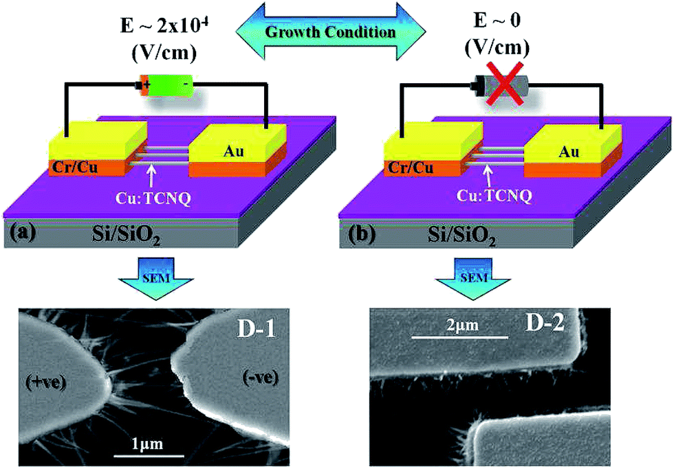 | ||
| Fig. 1 Schematic of the device for in-plane growth of Cu:TCNQ NW within prefabricated pads (a) with and (b) without field. The SEM images of Cu:TCNQ NWs corresponding to the growth conditions are indicated by arrows. | ||
The Cu:TCNQ NWs grown by this method consist of more conducting Phase-I Cu:TCNQ,19 as confirmed by X-ray diffraction (XRD) and Transmission Electron Microscopy (TEM). Generally metal:TCNQ complexes crystallize in Phase-I when the TCNQ stacks are ordered face to face during growth, leading to a one dimensional (1D) structure and enhanced conductivity. The data are shown in Fig. 2. From the Fourier transform infrared spectroscopy (FTIR) data and the observed shift in the –CN– stretching band we obtained an average charge transfer value (Z) of ≈0.5 for the Cu:TCNQ NWs grown by vapour phase.20
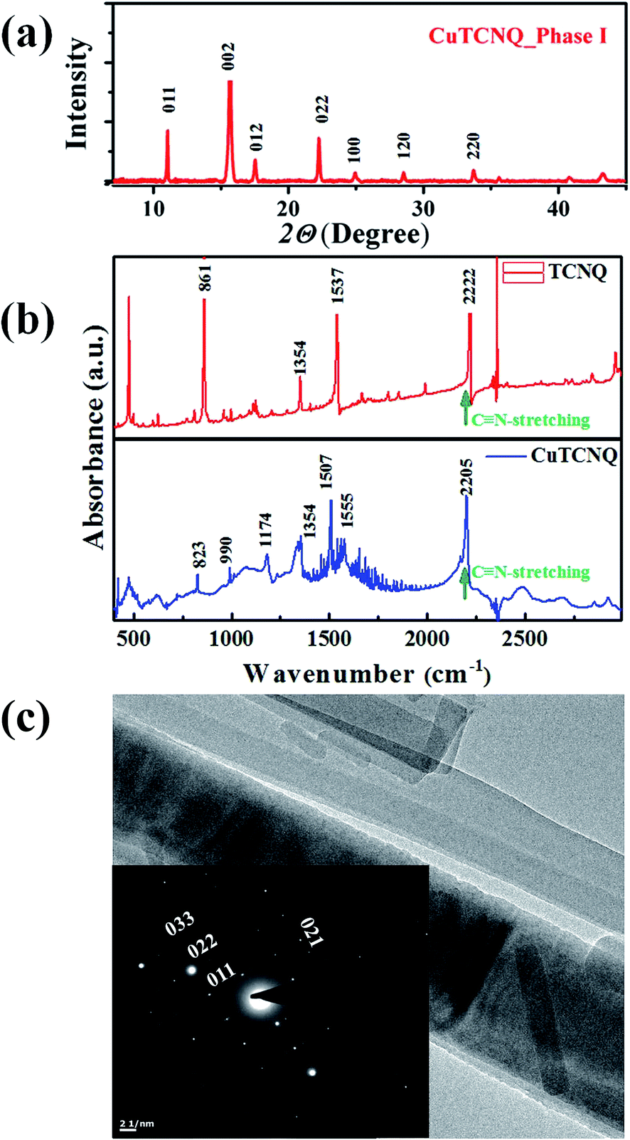 | ||
| Fig. 2 (a) X-ray diffraction patterns of PVD grown NWs. The indexing is as per the ICDD database. (b) FTIR spectra of TCNQ and Cu:TCNQ. The shift in the –CN– stretching mode gives the degree of charge transfer Z estimated from ref. 20. (c) TEM image of Cu:TCNQ NW dispersed on a TEM grid. (Inset) selected area electron diffraction (SAED) pattern of the NW to show its single crystalline nature. | ||
In the nanobridges, since the wires are connected to the electrodes, one can take direct measurements of the I–V curves. The bias dependent conductance G(V) was obtained by differentiating the I–V curves numerically  The measurements were done using a Source-meter (Keithley SM 2400) in a variable temperature insert in a Closed Cycle Refrigerator down to 40 K. The measurements were performed at ≥40 K because below that temperature the nanobridges are prone to mechanical failure. The nanobridges withstand thermal cycling reproducibly in the temperature range of 40 K to 300 K.
III. Results
An assortment of the I–V characteristics of both the NW samples measured over the temperature range 40 to 300 K are shown in Fig. 3. The data are plotted in a semi-log scale to accentuate the current in the low bias region. The figure shows that the nature of transport in the two types of NWs is somewhat different. The field grown NWs have higher conductance. The NWs show linear (symmetric) I–V curves at low bias but beyond the threshold voltage Vth, the I–V curves become strongly non-linear. (Note: the bias V used for the measurement is distinct from that used for growth.) The extent of non-linearity is also different in the two types of NWs. The I–V data taken at different temperatures show that there is a change in the conductance behaviour below 100 K where it becomes strongly non-linear and the threshold becomes more pronounced (data highlighted by circles and arrows). We show below that the strongly non-linear behavior may be related to CDW type transport.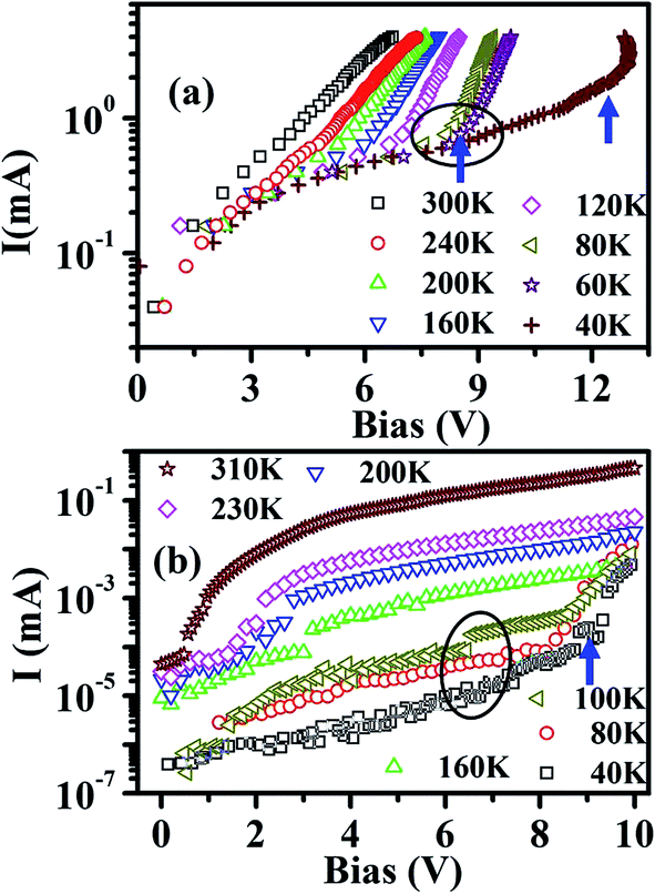 | ||
| Fig. 3 The I–V data at different temperatures of NWs grown (a) with field, E ∼ 2 × 10⁴ V cm−1, and (b) without field, E ∼ 0 V cm−1. The Vth for temperatures T < 100 K are marked by circles and arrows. | ||
The non-linear character of the transport beyond a threshold bias can be seen more clearly in the bias dependence of the conductance (G) as shown in the G–E curves shown in Fig. 4, where E is the field  The data shown have been scaled by the number of bridging wires in the nanobridge so that the value of the conductance G represents the conductance value of a single NW. It can be seen from the data that the conductance of the wires grown in the presence of the electric field (sample D-1) is larger by at least one order compared to that of the NWs grown by the same method but with zero field (sample D-2). The bias dependent G values taken at different temperatures also show that the nature of the dependence of G on E changes for T < 100 K. We will discuss this issue in detail later on.
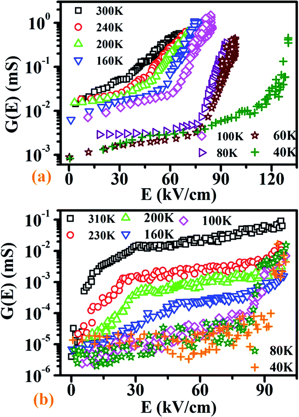 | ||
| Fig. 4 Bias dependent conductance G = dI/dV of NWs grown (a) with and (b) without field. The value of G has been scaled by the number of wires so that G represents the conductance of a single NW. | ||
Both the NWs show semiconducting behaviours and the conductance G reduces on cooling. However, the reduction is much stronger for the zero field grown NWs. In case of the field grown sample D-1, the reduction on cooling is rather shallow. The limiting low bias conductance G0  for the zero field grown sample at room temperature is ≈5 µS so that
 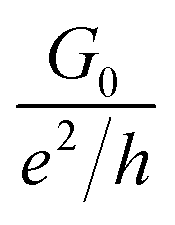 is ≈1/8, signifying that the NW strands are deep into the insulating state, justifying a substantial reduction of G0 on cooling. However, for the NWs grown in a field at room temperature the value of
  is ≤1. Thus, the NW strands grown in a field are on the verge of undergoing an insulator–metal transition. The application of a field during growth thus drives the NWs close to the transition boundary.
We have observed resistive state switching with hysteresis in the Cu:TCNQ NWs at a field of E ∼ 1.4 × 10⁵ V cm−1. Since the phenomenon of switching is not within the scope of the paper, the applied bias voltage has been kept lower than this value for measurement. However, even in the relatively lower bias, a strong dependence of G(E) on the bias E can be observed. The onset of non-linearity is distinct from switching with hysteresis. The thresholds for non-linear conduction, Eth, of both the samples are enhanced as the temperature of the measurement is reduced. We will do quantitative analysis of the non-linear part of the data later on.
The results presented above clearly show that when an electric field is applied to the NWs during growth, the conductivity of the NWs thus grown are strongly modified. The modification occurs in the linear conductance, temperature dependence and also in the non-linear part of the conductance. The experiment establishes the enabling role of the applied electric field during growth. It can thus act as a tool to control the resulting conductance of the NWs. The fact that the experiments were carried out in a nanobridge enabled us to reach conclusions about the conductance change at the level of a single NW. Experiments carried out on a bundle or a film of such NWs would not have allowed us to reach a clear conclusion.
IV. Discussion
A. Analysis of the conductance data with linear and non-linear parts
The observed conductance of both the NW samples, contain a linear part (bias independent conductance) and a strong non-linear part when the applied bias crosses a threshold. One of the models that has been proposed for such a one-dimensional system is the formation of a Luttinger liquid where I has a power law dependence on V with I ∝ VTα at low bias and I ∝ Vβ+1 at high bias,24 usually with α ≫ β. There are reports that non-linear conduction in Cu:TCNQ may follow such a relation.24 This was based on data taken over the T range of 330 K to 105 K.24 On extending the data to lower temperatures this does not remain valid. Instead there is a signature of a clear threshold for transport and a bias dependent G; both the NW samples show behavior that is different from that expected for a Luttinger liquid.One of the mechanisms that can give rise to non-linear transport with a threshold is CDW transport. In the related system of the charge transfer complex TTF:TCNQ there is a clear signature of CDW transport in bulk single crystals25 and films,26,27 as well as in NWs.8 In such a system the CDW transport occurs due to Peierls transitions in TTF and TCNQ stacks below 50 K.28 The NWs of TTF:TCNQ in which such a CDW transport was observed were grown from the vapour phase between pre-grown contact pads, as has been done here.8,29 Though no CDW type transport or Peierls transition in Cu:TCNQ has been reported to date, we investigated whether the non-linear transport can be described by such a scenario. Since the conductivity of Cu:TCNQ was not measured below 100 K before, it may be the reason that such a phenomenon was not observed or reported. Interestingly, there are theoretical studies using the Hubbard model which show that in alkali metal TCNQ salts like Na:TCNQ or K:TCNQ, the CDW phase can occur due to Peierls transition if the nearest neighbour interaction exceeds a certain critical value.30
The transport in the Cu:TCNQ NWs has a linear part G0 and a bias dependent non-linear part which we write as:
| G(E) = G0 + G1f(E) | (1) |
| f(E) = (E − Eth)γ | (2) |
 | (3) |
The fit of the data to eqn (3) has been shown for the data at 40 K for both the samples in the inset of Fig. 5, where we show the value of the scaled function  vs. the ratio
  Fig. 5 shows all the data for both the samples below 100 K plotted in the scaled curves. It can be seen that for both the samples, the functional form given by eqn (3) remains valid.
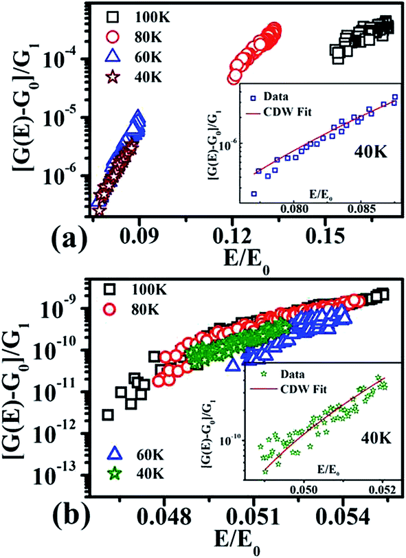 | ||
| Fig. 5 The non-linear part of conductance for the NWs grown (a) with and (b) without field at different temperatures fitted to the modified Zener tunneling relation. Insets in (a) and (b) indicate the CDW fit at 40 K. | ||
The linear conductance G0 for the whole temperature range (300–40 K) is shown in Fig. 6. The parameters of the fit, namely G1, Eth and E0 are shown in Fig. 7 as a function of temperature (below 100 K). A number of observations can be noted from Fig. 7 that reflect both the similarity and differences between the two NW samples. It is also interesting that in both the samples, the non-linear conduction (with threshold) for ≤100 K, can be described by eqn (3). Though there is a qualitative similarity between the parameters of the non-linear conduction in the two samples, there are important quantitative differences between the two sets of parameters belonging to the two samples. It needs to be emphasized that, though the non-linear conduction in both the samples follows eqn (3) which is associated with CDW transition, we are not in a position to firmly claim that the non-linear conduction so observed indeed originates from CDW related phenomena. However, there does exist a possibility, as discussed before, of a Peierls transition in the TCNQ stacks in Cu:TCNQ leading to the formation of CDW. This, however, would need independent support from temperature dependent structural data.
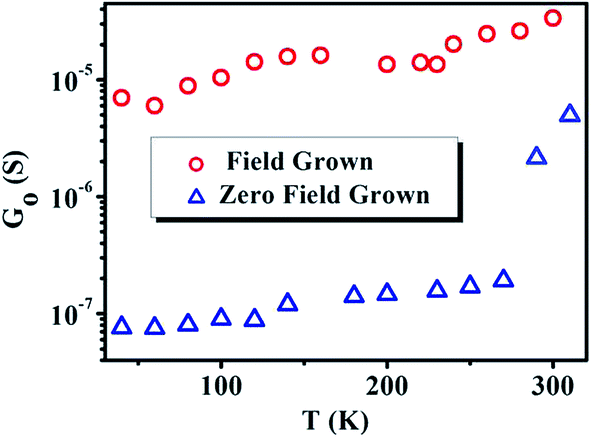 | ||
| Fig. 6 Temperature dependence of the linear conductance G0 (calculated from the slope of linear region of I–V) for field grown and zero field grown NWs. | ||
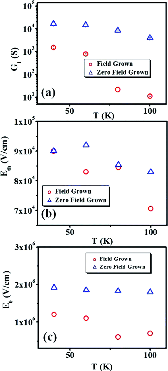 | ||
| Fig. 7 Temperature dependence of the parameters (a) G1, (b) Eth and (c) E0 as obtained from the fit to the modified Zener tunneling relation as shown in Fig. 5. | ||
B. Linear conductance and the temperature dependent resistivity
The values of the field independent conductance G0 differ significantly in the two samples. This is shown in Fig. 6. Near room temperature the field grown wires (D-1) have a conductance that is about one order more than that of the zero field grown NWs (D-2), as stated before. However, due to the steep temperature dependence of the more insulating NWs in D-2, G0 of the two differs by nearly 2 orders at 100 K. There are also certain qualitative observations that can be made from the temperature dependences of G0 of the two NW samples. The initial G0 decreases from 300 K down to the 250 K region for both the samples, although this is steeper for the zero field grown NW. However, there is a temperature independent plateau for both the samples below the 220 K region down to about 125 K where they again show a gradual decrease on cooling. From the conductance G0 we obtain the resistivity (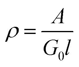 , A = area, l = length of the NW). We find that ρ shows activated behavior following a variable range hopping (VRH) relation for a disordered 1D system24,31,32 for the temperature range down to 200 K:
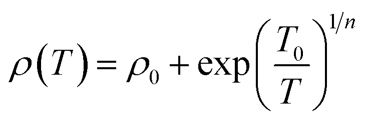 | (4) |
 a being the interatomic distance. The fit parameters are given in Table 1. For both the samples, the VRH eqn holds above 200 K and it deviates below this temperature. In the high temperature region where the VRH equation holds, the value of from this T0 reduces from 6300 K (≈520 meV) in D-2 to around 1625 K (≈135 meV) in D-1. The reduction of the value of T0 in the field grown sample points to a reduction in disorder. Reduction of the disorder will enhance the localization length so that α decreases. The reduction of disorder will also decrease the spread Δ. Both these factors will lead to a decrease in T0. The inference we can obtain from the data is that, on application of the electric field during growth, the order in TCNQ is enhanced. We will see below that this likely arises from increasing the order in the stacking of the TCNQ.
| Synthesis condition | Fitted parameters | |
|---|---|---|
| ρ 0 (Ω cm) | T 0 (K) | |
| Field grown | ∼1.05 × 10⁻³ | ∼1626 |
| Zero field grown | ∼6.69 × 10⁻⁷ | ∼6300 |
C. Parameters of non-linear conductance with threshold
The non-linear part of the conductance, whose weight we measure by G1, shows a strong rise on cooling. The parameters for fitting to the modified Zener model (eqn (3)), E0 and Eth, both show an enhancement on cooling. For the zero field grown sample (D-2), G1 changes by nearly one order on cooling from 100 K to 40 K tending to a temperature independent value at lower T. In the same region, the G1 for the field grown NWs (D-1) changes steeply by around 2 orders. Interestingly, the value of G1 for D-1 stays smaller than that of D-2, which is opposite to what has been observed for G0, which is distinctly higher for the field grown sample D-1.The existence of a distinct threshold field is seen in both the samples and Eth enhances on cooling. Interestingly, the values of Eth for the samples are very close. An enhancement of Eth on cooling has been observed in other systems that also show a CDW type transition.8 The parameter E0 also increases on cooling for both the samples, and more steeply for the field grown sample. For the zero field grown sample, E0 is larger and has a relatively shallow T dependence.
It will be worthwhile to compare the parameters E0 and Eth seen for Cu:TCNQ with those observed in NWs of a system like TTF:TCNQ that are known to show Peierls transitions. The value of the ratio  is an important parameter and gives the ratio of the tunneling length Lt to the coherence length of the CDW system ξ0 so that
 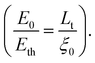 The value of the ratio is ≈2–5 for clean CDW systems like NbSe3.33 For NWs like TTF:TCNQ it is ≈10 at low temperatures. For the field grown Cu:TCNQ NWs, at 40 K the ratio is 10, while it is ≈20 for the zero field grown NWs. The field E0 ∼ ξ0−1 and Eth ∼ Lt−1. Since for both the NWs Eth is nearly the same, the larger value of the ratio for the zero field grown sample most likely arises due to the smaller coherence length ξ0. The coherence length ξ0 is ∝ Eg−1, where Eg is the pinning gap of the CDW. The application of the field, if it leads to a better alignment of the TCNQ stacks, can lead to a reduction of Eg and hence an enhancement of ξ0 and a smaller E0. The smaller value of the field E0 in the field grown sample may thus be justified within the framework of CDW transport.
To conclude this part, we observe that, whatever be the origin of the strong non-linearity, it is present in both samples but it is affected by the field applied during growth. The strong non-linearity appears to follow the transport behavior of a CDW system.
D. Suggested scenario for the effect of an applied electric field during growth leading to a change in the conductivity of the nanowire
In Cu:TCNQ there are two distinct factors (likely interdependent) that can alter its conductivity. The first is the stacking alignment of the TCNQ molecules and the second is the degree of charge transfer (Z). It is thus likely that any modification of one or both of the above will lead to a change in the conductivity of the charge transfer complex. The applied electric field during growth can affect both the processes. Based on this we propose the following likely scenario for our observation that the growth of the Cu:TCNQ NW in an electric field enhances its conductivity.The growth model of Cu:TCNQ from the vapour phase has not been worked out in detail. In the vapour phase growth, the length grows over time following a time dependence that originates from the diffusion of ionic species (length, l ∝ t), while the diameter does not change after the initial growth period. This diameter constrained growth is very similar to growth in solution where anodized alumina oxide (AAO) templates have been used to limit lateral growth.34 For both the growth processes two phenomena are involved after the initial nucleation phase (see the schematic in Fig. 8). There is a diffusion of Cu1+ ions from the Cu electrode through the growing wire to the open growth face. There is also diffusion of electrons from the Cu electrode (due to the redox potential) to the top growing surface, leading to oxidation of the arriving TCNQ molecules to TCNQ1−, which then reacts with the diffusing Cu1+ ions to make Cu:TCNQ. The efficiency of the process (ionic diffusion, as well as electron transport from the Cu side to the growth face) would determine the extent of the charge transfer Z. The application of an electric field during the growth process will enhance the Cu ion migration from the Cu electrode to the NW tip, thus facilitating the extent of the charge transfer and enhancing Z. In general the Cu:TCNQ NWs grown have Z ≈ 0.5–0.6. We have shown that a small increment in Z using materials such as graphitic oxide can lead an enhancement in conductivity by an order of magnitude.35 Thus an enhanced Z, enabled by the applied electric field during growth can increase the conductivity in the field grown wire substantially, as observed.
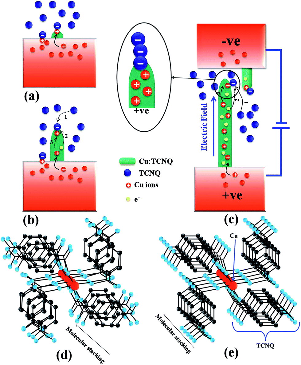 | ||
| Fig. 8 Schematic of Cu:TCNQ NW growth under an externally applied field. (a) Nucleation of the ions, (b) NW growth and (c) accelerated nucleation process under field. Stacking of the Cu:TCNQ molecules during growth (d) without field and (e) with field. Field grown NWs have better π–π stacking of the TCNQ molecules. | ||
The conductivity of the grown nanowire would also critically depend on the alignment of the TCNQ stacks in the NWs. As the NW grows from the vapour phase with the arrival of TCNQ molecules, the successive molecules, due to randomization by thermal forces, may not have the proper alignment. This lack of a proper alignment would lead to improper arrangements of the TCNQ stacks which will lead to lower conduction even if the grown wires are predominantly Phase-I. The application of the electric field, due to the highly anisotropic polarizability α (as in a TCNQ molecule), can lead to a torque that will align the arriving TCNQ molecules, leading to proper stacking. Such a polarization anisotropy induced alignment has been observed in the aligned growth of carbon nanotubes from the vapour phase in the presence of an applied field. The polarization anisotropy driven torque overcomes the randomizing effect of the thermal field leading to ordered growth.36 In Cu:TCNQ, the field driven enhancement in the order of stacking of TCNQ will enhance the conductivity and will also increase the coherence length ξ0 for the CDW phase. We do observe in our experiments that NWs grown in an electric field show larger ξ0 and thus lower threshold fields, Eth. The scenario suggested above, though qualitative, can explain the observation that the field applied during growth can indeed change the conductivity of the NWs.
V. Conclusion
In conclusion, we have shown that the application of an electric field during vapour phase growth can be a viable tool to enhance/modify the conductivity of NWs. The electrical conductance of the NWs (measured) down to 40 K shows a strong non-linear conductance which has a well defined threshold for T ≤ 100 K. The non-linear conductance was found to follow a modified Zener tunneling model proposed for CDW transport. Such an observation was not made before in Cu:TCNQ and opens up the possibility of a new investigation of CDW transport in this system.The application of the field during growth significantly enhances the conductance and, for a single NW grown in field, the conductance is close to  the boundary of the insulator–metal transition. The parameters of the non-linear conductance also change when the wire is grown in an electric field.
We proposed a scenario for the field growth condition where the applied field helps the diffusion of Cu+ ions from Cu to the growing face, leading to an enhanced charge transfer which results in enhanced conductivity. The field applied during growth has been proposed to improve the stacking of the TCNQ moiety, leading to an enhancement of conductance and also a change in the parameters of the non-linear conduction. Though the experiment has been done in the context of a charge transfer complex NW, the concept may have application in the growth of other semiconducting NWs.
Acknowledgements
The authors acknowledge the financial support from the Department of Science and Technology, Government of India as a sponsored project as Unit for Nanoscience (UNANST-II). They also acknowledge help from Dr K. Das in electron beam lithography. A. K. R. acknowledges J.C. Bose Fellowship for additional support.References
- L. Ma, J. Wang, J. Yip and F. Ding, J. Phys. Chem. Lett., 2014, 5, 1192–1197 CrossRef CAS PubMed
.
- A. Roy, T. Pandey, N. Ravishankar and A. K. Singh, J. Phys. Chem. C, 2014, 118, 18676 CAS
- C. Wang, Y. Hu, C. M. Lieber and S. Sun, J. Am. Chem. Soc., 2008, 130, 8902 CrossRef CAS PubMed
- C. Durkan and M. E. Wallend, Phys. Rev. B: Condens. Matter Mater. Phys., 2000, 61, 14215 CrossRef CAS
- A. Bid, A. Bora and A. K. Raychaudhuri, Phys. Rev. B: Condens. Matter Mater. Phys., 2006, 74, 035426 CrossRef
- P. A. Smith, C. D. Nordquist, T. N. Jackson, T. S. Mayer, B. R. Martin, J. Mbindyo and T. E. Mallouk, Appl. Phys. Lett., 2000, 77, 1399 CrossRef CAS PubMed
- D. Gates, Nat. Nanotechnol., 2010, 5, 484 CrossRef PubMed
- T. Phanindra Sai and A. K. Raychaudhuri, Nanotechnology, 2010, 21, 045703 CrossRef PubMed
- J. E. Fischer, W. Zhou, J. Vavro, M. C. Llaguno, C. Guthy, R. Haggenmueller, M. J. Casavant, D. E. Walters and R. E. Smalley, J. Appl. Phys., 2003, 93, 2157 CrossRef CAS PubMed
- T.-I. Jeon, K.-J. Kim, C. Kang, S.-J. Oh, J.-H. Son, K. Hyeok An, D. Jae Bae and Y. H. Lee, Appl. Phys. Lett., 2002, 80, 3403 CrossRef CAS PubMed
- C. Zhao and A. M. Bond, J. Am. Chem. Soc., 2009, 131, 4279–4287 CrossRef CAS PubMed
- J. Bardeen, Phys. Rev. Lett., 1979, 42, 1498 CrossRef CAS
- J. Bardeen, Phys. Rev. Lett., 1980, 45, 1978 CrossRef CAS
- R. S. Potemeber and T. O. Poehler, Appl. Phys. Lett., 1979, 34, 405 CrossRef PubMed
- R. Müller, S. Jonge, K. Myny, D. J. Wouters, J. Genoe and P. Heremans, Solid State Electron., 2006, 50, 601 CrossRef PubMed
- K. Wang, X. Qian, L. Zhang, Y. Li and H. Liu, ACS Appl. Mater. Interfaces, 2013, 5, 5825 CAS
- R. Basori, K. Das, P. Kumar, K. S. Narayan and A. K. Raychaudhuri, Opt. Express, 2014, 2, 4944 CrossRef PubMed
- J. Billen, S. Steudel, R. Müller, J. Genoe and P. Heremans, Appl. Phys. Lett., 2007, 91, 263507 CrossRef PubMed
- R. A. Heintz, H. Zhao, X. Ouyang, G. Grandinetti, J. Cowen and K. R. Dunbar, Inorg. Chem., 1999, 38, 144 CrossRef CAS
- J. S. Chappell, A. N. Bloch, W. A. Bryden, M. Maxfield, T. O. Poelher and D. O. Cowan, J. Am. Chem. Soc., 1981, 103, 2442 CrossRef CAS
- A. P. O’Mullane, N. Fay, A. Nafady and A. M. Bond, J. Am. Chem. Soc., 2007, 129, 2066 CrossRef PubMed
- C. A. Fernandez, P. C. Martin, T. Schaef, M. E. Bowden, P. K. Thallapally, L. Dang, W. Xu, X. Chen and B. P. McGrail, Sci. Rep., 2014, 4, 06114 CrossRef CAS PubMed
- Z. Zhou, R. Jin, G. Eres, A. Subedi and D. Mandrus, Appl. Phys. Lett., 2006, 89, 133124 CrossRef PubMed
- Z. Zhou, K. Xiao, R. Jin, D. Mandrus, J. Tao, D. B. Geohegan and S. Pennycook, Appl. Phys. Lett., 2007, 90, 1931151 Search PubMed
- M. J. Cohen and A. J. Heeger, Phys. Rev. B: Solid State, 1977, 16, 688 CrossRef CAS
- R. Springell, R. C. C. Ward, J. Bouchet, J. Chivall, D. Wermeille, P. S. Normile, S. Langridge, S. W. Zochowski and G. H. Lander, Phys. Rev. B: Condens. Matter Mater. Phys., 2014, 89, 245101 CrossRef
- P. Goli, J. Khan, D. Wickramaratne, R. K. Lake and A. A. Balandin, Nano Lett., 2012, 12, 5941 CrossRef CAS PubMed
- V. Solovyeva and M. Huth, Synth. Met., 2011, 161, 976 CrossRef CAS PubMed
- T. Phanindra Sai and A. K. Raychaudhuri, Mater. Res. Soc. Symp. Proc., 2008, 1058, JJ05-03 Search PubMed
- M. Kumar, B. J. Topham, R. Yu, Q. B. D. Ha and Z. G. Soos, J. Chem. Phys., 2011, 134, 234304 CrossRef PubMed
- A. N. Bloch, R. B. Weisman and C. M. Varma, Phys. Rev. Lett., 1972, 28, 753 CrossRef CAS
- M. M. Fogler, S. V. Malinin and T. Nattermann, Phys. Rev. Lett., 2006, 97, 096601 CrossRef
- L. Sneddon, M. C. Cross and D. S. Fisher, Phys. Rev. Lett., 1982, 49, 292 CrossRef CAS
- H.-X. Ji, J.-S. Hu, Y.-G. Guo, W.-G. Song and L.-J. Wan, Adv. Mater., 2008, 20, 4879–4882 CrossRef CAS PubMed
-
R. Basori and A. K. Raychaudhuri, accepted in IEEE Explore Conference Proceeding, 2014 Search PubMed
- Y. Avigal and R. Kalish, Phys. Lett., 2001, 78, 2291 CAS
| This journal is © The Royal Society of Chemistry 2015 |