
Versatility and robustness of ZnO:Cs electron transporting layer for printable organic solar cells
Abstract
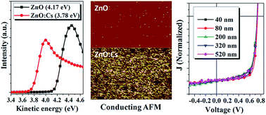
In this work, a Cs doped sol–gel ZnO film (ZnO:Cs) as an efficient and robust electron transporting layer (ETL) in versatile systems of organic solar cells (OSCs) is developed, which can be simply formulated by blending the Cs2CO3 with the Zn(Ac)2 precursor in solutions. The Cs doping significantly increased the ZnO film conductivity and lowered its work function, as unveiled by the conductive atomic force microscope and the ultra-violet photoelectron spectroscopy. Decent device performance enhancements of OSCs with versatile photovoltaic materials, e.g. P3HT : PC61BM, P3HT:ICBA, and PTB7 : PC71BM, were observed with the doped ZnO:Cs as the ETL compared with the pristine ZnO ETL. The enhanced device performance was also found in the tandem solar cells. Moreover, the device performance shows little drop with the thickness of the doped ZnO:Cs ETL ranging from 40 to 520 nm, indicating the less thickness dependence for the doped ZnO:Cs ETL. The current work verifies the potential of the Cs doped ZnO as a high performance ETL material for printable OSCs.
 Please wait while we load your content...

