Improve piezoelectricity and elasticity of Ce-doped BaTiO3 nanofibers — towards energy harvesting application

Yongyong Zhuang*a, Zhuo Xu*a, Fei Lia, Zhipeng Liaob and Weihua Liub
aElectronic Materials Research Laboratory, Key Laboratory of the Ministry of Education and International Center for Dielectric Research, Xi'an Jiaotong University, Xi'an, 710054, China. E-mail: xuzhuo@mail.xjtu.edu.cn
bVacuum Microelectronic and Microelectronic Mechanical Institute, Xi'an Jiaotong University, Xi'an, 710049, China

Received 28th April 2015 , Accepted 16th June 2015

First published on 16th June 2015


Abstract

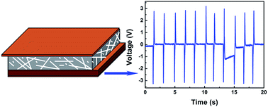
Ce-doped BaTiO3 (BTO) nanofibers were prepared by sol–gel combined with electrospinning method. The influence of cerium ions concentration on BTO crystal phase, microstructure, piezoelectricity, and elasticity were investigated. The energy harvesting properties of the device based on Ce-doped BTO nanofibers were tested. The piezoelectric property of BTO nanofibers were improved after cerium doping. The elastic property of the fibers changed little after cerium doping. The elastic modulus of the pure BTO nanofibers was about 3.37 GPa. When the Ce/Ba atomic ratio was 0.6%, the elastic modulus dropped to 1.18 GPa. Our analysis of the temperature range of the energy harvesting device indicates that an effective operation can be obtained when the working temperature of the device is below 110 °C. The largest delivered power of the energy harvesting device was 14.37 μW with a load resistance of 100 MΩ, when the Ce/Ba atomic ratio was 0.6%.


Introduction

Energy harvesting device towards self-powered nano/micro systems have been attracting increasing attention. Various energy harvesting devices have been fabricated, including nanogenerators,1–4 solar cells,5,6 thermoelectric cells,7 and hydrogen cells,8,9 etc. It is of special importance for many applications to harvest mechanical energy from the environment. The invention of nanogenerator opened a gate towards harvesting mechanical energy of various kinds from the environment. Among them, nanogenerators based on piezoelectric materials have aroused a lot of attention. Zinc oxide (ZnO)10,11 has been demonstrated as an example of piezoelectric material in harvesting energy from environmental mechanical energy, including heartbeats, blood flow, muscle stretching, and body movement. However, the low piezoelectric coefficient of ZnO material limits its application. Wu et al.12 reported a flexible and wearable PZT based nanogenerator fabricated by a simple method. This generator can generate 200 μW cm−3 output powers, large enough to power a liquid crystal display. However the lead content of PZT materials raises environmental concerns. Other materials such as 0.5Ba(Zr0.2Ti0.8)O3–0.5(Ba0.7Ca0.3)TiO3 (BZT–BCT),13 barium titanate (BT),14 sodium potassium niobate (KNN),15,16 and lead magnesium niobium titanate (PMNT)17 have also been reported. BaTiO3, as a valuable candidate piezoelectric material, has attracted our interest due to the following merits. First, BTO is an environmentally-friendly material (lead-free), it shows great potential for implantable biological devices. Second, a stable operation at room temperature requires the Curie temperature significant above the room temperature. BTO has a higher Curie temperature, which indicates a higher stability at higher temperatures. However, the power generated from BTO materials is not high enough for the practical application.14 Besides, the elasticity and Curie temperature of BTO nanofibers in nano size are still unclear. Thus, it is desperately urgent to find a way to improve the output signals, stability, and elasticity of BTO materials.

In this work, the Ce-doped BTO nanofibers were fabricated by an electrospinning process.18 The cerium ions were chosen to modify the piezoelectric property of BTO nanofibers. The crystal structure of Ce-doped BTO nanofibers was investigated. The piezoelectric and ferroelectric properties of the Ce-doped BTO nanofibers were characterized by PFM. The mechanical behaviors of single BTO nanofibers with different cerium concentration were investigated by Force–distance (F–d) curves. The Ce-doped BTO was used to construct energy harvesting devices by a simple method. The Ce concentration in BTO nanofibers has an effect upon the energy harvesting efficiency in terms of output voltage and current of these devices.

Materials and methods

Synthesis of Ce-doped BTO nanofibers

Ce-doped BaTiO3 (BTO) nanofibers with a Ce/Ba atomic ratio of 0–1.0% were prepared by sol–gel combined with electrospinning method.18 Analytical grade stoichiometric barium acetate (99.0%, Guangdong Guanghua Chemical Reagent Co. Ltd, Guangdong, China), tetrabutyl titanate (99.0%, Tianjin Hedong district Hongyan Chemical Reagent Factory, Tianjin, China) and cerium nitrate hexahydrate (Ce(NO3)3·6H2O) (99–100% Tianjin Fuchen Chemical Reagent Factory, Tianjin, China) with different concentration were used as starting materials. Proper citric acid (Analytical Reagent, 36%, Tianjin Tianli Chemical Reagent Co. Ltd, Tianjin, China) was added into the starting materials to balance hydrolysis and polymerization of the sol solution.18 The poly(vinyl pyrrolidone) (PVP, Mw = 1[thin space (1/6-em)]300[thin space (1/6-em)]000 Alfa Aesar) dissolved in ethanol solution (Analytical Reagent, Tianjin Dasen Chemical Reagent, Co. Ltd, Tianjin, China) was used to control the viscosity of the whole solution. The solution of Ce-doped BTO sol–gel mixed with PVP solution was actively stirred for 2 h to obtain a complete homogeneous solution. After the dissolution of all the compounds, the final viscous solution was electrospun by applying 1 kV cm−1 electric field, through a hypodermic syringe. A flat-plate collector was used to collect the electrospun fibers. The electrospun Ce-doped BTO nanofibers were finally annealed at 750 °C for 10 h.

Characterization

The crystal structure and morphology of the Ce-doped BTO nanofibers were analyzed by X-ray diffraction (XRD, D/max2200 Rigaku, Japan) and scanning electron microscope (SEM, Quanta FEG 250 FEI, USA), respectively. The elemental composition of Ce-doped BTO nanofibers was characterized by energy dispersive X-ray analysis (EDAX Quanta FEG 250 FEI, USA). Raman scattering of the Ce-doped BTO nanofibers was carried out using Raman spectroscopy (HR 800 HORIBA JOBIN YVON, France) with 20 mw at 514 nm. The effect of cerium concentration on the structure of BTO nanofibers was characterized by Fourier transform infrared spectroscopy (FTIR-8400S (CE) SHIMADZU, Japan). The microstructure of the nanofibers was investigated by the transmission electron microscope (TEM JEM 2100 JEOL, Japan). The output current and voltage signals of the energy harvesting device were collected by oscilloscope (3014B Tektronix, USA) combined with low-noise current preamplifier (SR 570 SRS, USA) and low-noise voltage preamplifier (SR 560 SRS, USA), respectively. The domain structure and piezoelectric properties of the nanofibers were characterized by piezoresponse force microscopy (PFM Cypher Asylum Research, USA). The elastic modulus and the topography of the Ce-doped BTO nanofibers were measured by atom force microscopy (AFM INNOVA Veeco, Germany) in air, at ambient conditions, using an SNL-10 scanning silicon probe, which was equipped with a silicon nitride cantilever. The radius, sensitivity and spring constant of the probe are 2 nm, 0.0439 μm V−1 and 0.038743 N m−1, respectively. The Curie temperature of the Ce-doped BTO nanofibers was characterized by differential scanning calorimetric (DSC) (NETZSCH STA 449C, Germany).

Results and discussion

Crystal structure and microstructure analysis of Ce-doped BTO nanofibers

Fig. 1 illustrates the XRD results of the BTO nanofibers with different cerium doping level. Well-defined perovskite patterns are observed after all the samples have been annealed at 750 °C for 10 hours. Some impurity barium carbonate peaks around 23° were observed. With the increased concentration of cerium, the peak position near 45° shifts slightly to higher angle, which indicates a decrease of the lattice volume. When the Ce/Ba atomic ratio is larger than 0.6%, the peak position near 45° begins to shift to lower angle. This indicates an increase of the lattice volume. The line shape of BTO diffraction peak at about 45° is sensitive to the phase structure. The split of BTO (200) diffraction peak is usually regarded as the signal of the formation of tetragonal BTO. However, the splitting peaks around 45° of all the samples are not obvious, which is probably induced by the broadening effects associated with fine crystalline grain size of the nanofibers. It is difficult to judge weather the phase structure is tetragonal or cubic from the XRD patterns.
image file: c5ra07750h-f1.tif
Fig. 1 X-ray diffraction patterns of BTO nanofibers with different Ce/Ba atomic ratio, all the fibers were annealed at 750 °C for 10 h. The right figure is a magnification of the peak around 45°.

Raman spectrum is an important method to investigate the crystal structure. The room temperature Raman spectra of the Ce-doped BTO nanofibers are shown in Fig. S1. The intensity of the two bands at 305 cm−1 and 717 cm−1 are believed to be correlated with the crystalline quality and the tetragonal phase of Ce-doped BTO nanofibers.19,20 It is apparent that all the samples have these two peaks as shown in Fig. S1. This indicates that the Ce-doped BTO nanofibers are tetragonal phase. The small broad mode ∼630 cm−1 is activated by the size effect of the BTO nanofibers.21 And the narrow 1060.6 cm−1 peak is attributed to the existence of BaCO3.20

The SEM images of electrospun Ce-doped BTO nanofibers calcined at 750 °C are shown in Fig. 2. As shown in the figure, all the fibers exhibit good surface morphology and uniformity in diameter. The average diameters of all the fibers are in the range of 100 nm to 200 nm. The lengths of the nanofibers are in the order of a few micrometers. The fibers continuity is maintained with different Ce/Ba atomic ratio after annealed at 750 °C. According to the above analysis, the Ce-doping could not raise the change of the surface morphology. No beads or holes could be seen in all the fibers, this means that all the samples are density.


image file: c5ra07750h-f2.tif
Fig. 2 SEM images of Ce-doped BTO nanofibers with Ce/Ba atomic ratio of: (a) 0; (b) 0.2%; (c) 0.4%; (d) 0.6%; (e) 0.8%; (f) 1.0%.

The TEM images and nano beam diffraction (NBD) pattern of a single BTO nanofiber with Ce/Ba atomic ratio of 0.6% is shown in Fig. 3. The fiber shows a straight cylindrical shape. The diameter is about 100 nm. The high resolution image of the fiber in Fig. 3(b) shows the crystalline of an individual grain. The interplanar spacing determined from the lattice fringe is about 2.847 Å, which corresponds to (1[1 with combining macron]0) planes of BaTiO3. The nano beam diffraction (NBD) pattern of the individual grain from the red disk of the fiber shown in Fig. 3(a) is consistent with a [[1 with combining macron][1 with combining macron][1 with combining macron]] zone axis for a tetragonal perovskite and is confirmed through crystallographic simulations using software (Crystal Maker. Single Crystal. v 2.0.1).


image file: c5ra07750h-f3.tif
Fig. 3 TEM images and nano beam diffraction (NBD) pattern of a single BTO nanofiber with Ce/Ba atomic ratio of 0.6%: (a) low magnification; (b) high resolution TEM image of the red disk of (a); (c) NBD pattern of the red disk of (a).

Fabrication of flexible energy harvesting device with the Ce-doped BTO nanofibers

The energy harvester based on Ce-doped BTO nanofibers consists of three layers as shown in Fig. 4. The copper clad laminate films (two copper layers and one intermediate Kapton layer, 120 μm total thicknesses) were chosen as the flexible substrate and bottom electrode. A mixture of Ce-doped BTO nanofibers and poly(dimethylsiloxane) (PDMS) in a mass ratio of 1[thin space (1/6-em)]:[thin space (1/6-em)]10 was spin-coated on the clean substrate at 3000 revolutions per minute (rpm), and heated for 30 min at 80 °C to obtain the piezoelectric potential layer. A copper foil (25 μm) was placed on the mixture layer as the top electrode. Two copper wires were attached to the bottom and top electrodes for easy testing. Before the characterization of the output signals, the energy harvester was poled in silicon oil at 130 °C by applying an electric field of 5 kV mm−1 for 30 min. Before the testing procedure, the devices are laid on the top surface of two slides. The two ends of the device are fixed to the slides. And there is no any object under the middle section of the device. The thickness of each slide is 2 mm. This means that the maximum magnitude of the deformation is 2 mm. During the testing process, the external force is applied on the surface of the device. And raise bending or stretching of the device. The schematic of this procedure can be seen in Fig. S2.
image file: c5ra07750h-f4.tif
Fig. 4 Schematic diagram of an energy harvesting device, where the two origin color layers of the upper left image are copper electrodes, the dark red color layer is Kapton; the white lines in the second image are the Ce-doped BTO nanofibers, the gray layer is the PDMS; The fourth image is the energy harvesting device.

The performances of the energy harvester

The performances of the flexible energy harvesting device fabricated by BTO nanofibers with different cerium concentration are investigated by short-circuit current and open-circuit voltage curves. Fig. 5 shows the output signal curves of the energy harvesting device based on Ce-doped BTO nanofibers. Fig. 5(a) shows the current output of the device fabricated with pure BTO nanofibers, the current is very low. This might be attributed to the lower piezoelectricity (d33 = 20 pm V−1 (ref. 18)) of pure BTO nanofibers. To exclude the possible effect of the electrode and PDMS layer, we fabricated the energy harvester which contains no BTO nanofibers (shown as in Fig. S3), the results show that the output maximal current is in the order of 0.2 pA, this value is much smaller than the value of Fig. 5(a). Fig. 5 (b)–(d) show the output voltage, current, and power with different Ce/Ba atomic ratios, respectively. The output signals keep increasing with the increase of cerium concentration. When the Ce/Ba atomic ratio is 0.6%, the max output is obtained. The largest output current and voltage signals are 434.2 nA and 3.28 V, respectively. The relevant output power density is 32.14 μW cm−3. The output voltage is slightly lower than the NG fabricated by BTO nanotubes (5.5 V),22 this could be relate to the morphology difference of fiber and tube of BTO materials. Fig. 5(e) and (f) show the output voltage and current of BTO nanofibers with the Ce/Ba atomic ratio of 0.6%. The output signals of BTO nanofibers with other cerium concentrations are shown in Fig. S4. The signals of Fig. 5(e) and (f) are obtained under different external forces and frequencies. The power delivered to the outer load under an external force is estimated using the following equation:23
 
image file: c5ra07750h-t1.tif(1)
where PL is the delivered power, V0(t) is the real-time voltage, RL is the resistance of the outer load, and T is the duration of external force application. The delivered power can be up to 14.37 μW with a load resistance of 100 MΩ.

image file: c5ra07750h-f5.tif
Fig. 5 Output signals of Ce-doped BTO nanofibers based energy harvesting devices: (a) short-circuit current of the device based on pure BTO nanofibers; open-circuit voltage (b), short-circuit current (c) and output power (d) of the devices based on BTO nanofibers with different Ce/Ba atomic ratio (0.2–0.8%); open-circuit voltage (e) and short-circuit current (f) of the device based on BTO nanofibers with the Ce/Ba atomic ratio of 0.6%.

Theoretical analysis

The high output signals of the energy harvesting device are caused by the improved piezoelectric property and carrier concentration of Ce-doped BTO nanofibers. It has been reported that the Ce-doping could enhance piezoelectric constant.24 The mechanism of cerium doping is complicated. The cerium ions could exist in BTO structure in Ce3+ and Ce4+ valance states, having a radii of 1.01 Å and 0.87 Å, respectively.25 Firstly, the A site Ba2+ will be replaced by Ce3+ as donor ions.26 This will induce cation vacancies when the cerium concentration is relatively low (the Ce/Ba atomic ratio is smaller than 0.6%). Ba2+ has a bigger ionic radius of 1.35 Å (ref. 27) than Ce3+ ions, which induces the decrease of the cell volume. The charge balance compensation mechanism may be described as below:
 
BaTiO3 + xCe3+ → Ba1−x2+(Ce˙Ba)xTi4+O32− + xV′′Ba (2)

The Ba-vacancies will effectively reduce the amount of oxygen vacancies, ease the movement of domain walls, and enhance the value of d33.28 The enhanced mobility of the carrier will effectively increase the output current of the energy harvester. The largest piezoelectric constant could be obtained when the Ce/Ba atomic ratio is 0.6%. Also, the largest output signals are obtained. When the Ce/Ba atomic ratio is larger than 0.6%, Ce4+ begins to isovalently substitute for Ti4+ (0.605 Å (ref. 25)) at the B sites. The Ce4+ pushes away of the six O2− from the original cell and converts the tetragonal structure to cubic structure, thus increasing the cell volume and decrease the magnitude of the spontaneous polarization and the piezoelectric constant.29 And the carrier concentration does not increase. For the above reason, the output signals decrease with the increase in the cerium ions concentration. The reaction formulas possibly happen as below:

 
BaTiO3 + xCe3+ + yCe4+ → Ba1−x2+(Ce˙Ba)x(Ti1−y4+(CeTi)y)O32− + xV′′Ba + yTi′′′′Ti (3)

Fourier transformation infrared spectroscopy (FTIR) is a sensitive method to characterize the change of various chemical bonds. The substituting type and the sites of cerium ions can be examined from FITR results. Fig. S5(a) shows the FTIR spectra of Ce-doped BTO nanofibers in the wavenumber range of 400–4000 cm−1. The strong absorption peaks near 520 cm−1 of all the samples are attributed to the stretching vibration of Ti–O band.30,31 The bands at 460 cm−1 and 440 cm−1 can be attributed to normal Ti–O bending vibrations. The influence of Ce concentration can be observed by investigating the absorption peak of the Ti–O bond at 460 cm−1 and 440 cm−1, where they are slightly shifted to higher or lower wavenumbers with various Ce concentrations. On the one hand, the corresponding peaks of the fibers shift to a higher wave number when the B–O (B[double bond, length as m-dash]Ti or Ce) bonds are enhanced. This means that the cerium ions will enter the A sites of BTO. On the other hand, they move to a lower wave number when the B–O (B[double bond, length as m-dash]Ti or Ce) octahedrons are distorted. This means that the cerium ions will enter the B sites of BTO. It can be seen that the characteristic wavenumbers slightly shift toward the high wavenumbers with increasing Ce concentration and begin to shift gradually toward the low wave numbers as the Ce/Ba atomic ratio grow until they are larger than 0.6%. This result is in well agreement with the doping mechanism discussed above. It can be inferred that the cerium will first substitute Ba2+ when the Ce/Ba atomic ratio is smaller than 0.6% and the cerium ions begin to substitute Ti4+ as the Ce/Ba atomic ratio is larger than 0.6%. Fig. S5(b) is the EDAX result of the Ce-doped BTO nanofibers with Ce/Ba ratio of 0.6%. The elemental composition of the nanofibers can be obtained. The cerium ions could be found from the figure. This means that the cerium ions are successfully enter the BTO lattice.

The piezoelectric and ferroelectric properties of the Ce-doped BTO nanofibers

The piezoresponse of the Ce-doped BTO nanofibers is characterized by PFM. Fig. 6 shows the PFM results of the Ce-doped BTO nanofiber. The Ce/Ba atomic ratio is 0.6%. The diameter of the fiber from Fig. 6(a) is on the order of 100 nm. The piezoresponse magnitude can be estimated from the amplitude image of Fig. 6(b). The phase image is shown in Fig. 6(c). The bright and dark regions in the whole fiber are corresponding to the domains oriented upwards and backwards directions, respectively. This means that the fiber is a ferroelectric material at room temperature. The piezoresponse amplitude loop and phase hysteresis are shown in Fig. 6(d) and (e). The vertical dc bias is swept from −20 V to 20 V. The variation of amplitude is equal to the change of strain under external electric field. The butterfly shape of the amplitude loop implies the existence of well defined polarizations along the vertical direction of the fiber. The complete saturation in the hysteresis loop with a bias of ∼18 V is observed. The maximum amplitude from Fig. 6(d) is 837 pm at 20 V. The calculated d33 at 20 V can be estimated to be 42 pm V−1, which is double as much as the pure BTO nanofibers.18 This implies that the doping of cerium ions will effectively improve the piezoelectricity of BTO nanofibers. Fig. 6(f) is the piezoresponse hysteresis loop of the fiber which is obtained from the following equation:
 
P = A[thin space (1/6-em)]cos[thin space (1/6-em)]θ (4)
where P is the piezoresponse signal, A is the piezoresponse amplitude, θ is the phase angle. The observed hysteresis loop show full switching of the polarization with coercive bias about 2.5 V and −4 V, respectively. The overall shift of the hysteresis loop toward to the negative side could be attributed to the polarization pinning due to either mechanical stress or charge trapping.32

image file: c5ra07750h-f6.tif
Fig. 6 PFM results of Ce-doped BTO nanofibers with the Ce/Ba atomic ratio of 0.6%: (a) topography image; (b) vertical amplitude image; (c) vertical phase image, the presence of ferroelectric domains in the entire fiber is obvious; (d) amplitude versus bias loop; (e) phase versus bias loop; (f) piezoresponse versus bias loop.

The piezoelectricity of the BTO nanofibers is originated from the movement of the domains. So, it's meaningful to study the ferroelectric domains. The ferroelectric domains of the fiber are observed by using the PFM. Fig. 7 shows the phase images of the fiber under different polarization voltages. The presence of ferroelectric domains in the entire fiber is clearly evident from theses figures. There is no phase change before the poling process (the applied voltage is 0 V) as shown in Fig. 7(a). The bright areas of the rectangle region in the figures increase with the increase of the applied voltage. The whole region show bright contrast when the applied bias is 40 kV. This implies that all the dipoles are aligned along with the direction of the applied voltage. A single domain is formed.


image file: c5ra07750h-f7.tif
Fig. 7 PFM phase images of a single BTO nanofiber with Ce/Ba atomic ratio of 0.6%. The images are obtained under different polarization bias: (a) 0 V; (b) 20 V; (c) 30 V; (d) 40 V.

The elastic modulus of the energy harvester

The elastic modulus of BTO based nanofibers is important for flexible energy harvesting device. A commercial AFM was used for the nanoindentation experiments on the Ce-doped BTO nanofibers. The experimental setup for the indentation measurements is sketched in Fig. 8(a). A one to one relationship between Fig. 8(a) and (b) are listed by using Arabic numerals. As the cantilever approaches the surfaces (in the noncontact region) of the sample, a force deflection is measured, indicating the existence of some long-range attractive/repulsive forces. After jumping into contact condition, if the cantilever is sufficiently stiff, the probe tip indents into the surface and provides information about the local elasticity. The force was found to increase linearly with the increase in distance. Fig. 8(b) displays the AFM images of Ce-doped BTO nanofibers. The Ce/Ba atomic ratios are 0.0 and 0.6%, respectively. The force–distance curves are obtained by indenting on the substrate and the nanofibers. The diameters of the two fibers are on the order of 80 nm. The estimated elastic modulus of the fibers with Ce/Ba atomic ratio of 0.0 and 0.6% are 3.37 GPa and 1.18 GPa, respectively, when the applied load is 10 nN. The two values are very close, this means that the Ce-doping change the elastic modulus of BTO nanofibers little.
image file: c5ra07750h-f8.tif
Fig. 8 Schematic of the approach–retract cycle of the AFM tip, the Arabic numerals in (a) are corresponding to the Arabic numerals in (b): 1 the AFM tip is approaching the fiber surface; 2 the initial contact between the tip and the surface, the attractive van der Walls forces lead to an bending of the cantilever toward the surface; 3 the bending cantilever return to its initial state as the fiber surface approach to the tip; 4 an indentation appears; 5 the tip begin to retract from the fiber surface; 6 the adhesive force lead to an bending of the cantilever as the tip continuous retract form the fiber surface; 7 the tip withdraws and looses contact to the fiber surface. (b) is the Force–distance curves of the silicon substrate and BTO nanofibers with Ce/Ba atomic ratios of 0.0% and 0.6%, respectively. The left inset figures are the AFM images of BTO nanofibers with Ce/Ba atomic ratio of 0.0% and 0.6%, respectively.

The effective working temperature range of the energy harvester

These energy harvesters can only work under Curie temperature Tc. When the temperature is higher than Tc, a paraelectric structure of the Ce-doped BTO nanofibers appears, and no piezoelectric response can be observed. The Curie temperature of BTO nanofibers may be different from the bulk materials as their size down to nano scale. Fig. S6 shows the results of DSC analysis of the Ce-doped BTO nanofibers. The Ce/Ba atomic ratios are 0.0 and 0.6%, respectively. The Curie temperature Tc, know as the phase transition temperature, can be observed from the peak of the DSC curves. The peak of pure BTO nanofibers shows that the tetragonal-cubic phase transition occurred at 124.5 °C. A weak broad peak of phase transition was also observed in the range of 110–136 °C in the Ce-doped BTO nanofibers. This is caused by the weak tetragonal structure of the Ce-doped BTO nanofibers (the calculated c/a ratio from XRD is only 1.0017 for BTO nanofibers when the Ce/Ba atomic ratio is 0.6%.). The above analysis suggests that an effective operation can be maintained when the working temperature of the device is lower than 110 °C.

Conclusions

Ce-doped BTO nanofibers were successfully prepared by sol–gel combined with electrospinning method. All the Ce-doped BTO nanofibers show tetragonal phases. The SEM study reveals that all the fibers have good surface morphology. The diameters of BTO nanofibers are in the order of hundreds nanometers. The TEM study reveals the prepared nanofibers are multicrystal. The elastic modulus of the pure BTO nanofibers is 3.37 GPa. The value is 1.18 GPa for Ce-doped BTO nanofibers when the Ce/Ba atomic ratio is 0.6%. It indicates that the fibers are flexible. The DSC results suggest that the an effective operation can be obtained when the working temperature is lower than 110 °C. The Ce-doping can improve the output signals. When the Ce/Ba atomic ratio is 0.6%, the largest delivered power of the energy harvesting device can be up to 14.37 μW with a load resistance of 100 MΩ.

Acknowledgements

The work was supported by the National Nature Science Foundation of China (Grant nos 51102193 and 51372196), China Postdoctoral Science Foundation (Grant no. 2012M521761 and 2014T70914), 111 Project B14040 and National Basic Research Program of China (973 Program) under Grant no. 2015CB654602.

Notes and references

  1. A. F. Yu, M. Song, Y. Zhang, J. Z. Kou, J. Y. Zhai and Z. L. Wang, Nanotechnology, 2014, 25, 455503 CrossRef PubMed.
  2. L. Gu, N. Y. Cui, L. Cheng, Q. Xu, S. Bai, M. M. Yuan, W. W. Wu, J. M. Liu, Y. Zhao and F. Ma, et al., Nano Lett., 2013, 13, 91–94 CrossRef CAS PubMed.
  3. Y. F. Li, G. Cheng, Z. H. Lin, J. Yang, L. Lin and Z. L. Wang, Nano Energy, 2015, 11, 323–332 CrossRef CAS PubMed.
  4. L. Lin, Y. N. Xie, S. M. Niu, S. H. Wang, P. K. Yang and Z. L. Wang, ACS Nano, 2015, 9, 922–930 CrossRef CAS PubMed.
  5. M. Y. Bashouti, M. Pietsch, G. Bronstrup, V. Sivakov, J. Ristein and S. Christiansen, Prog Photovolt Res Appl., 2014, 22, 1050–1061 CrossRef CAS PubMed.
  6. S. K. Kim, S. Park, M. K. Son and H. J. Kim, Electrochim. Acta, 2015, 151, 531–536 CrossRef CAS PubMed.
  7. A. I. Boukai, Y. Bunimovich, J. T. Kheli, J. K. Yu, W. A. Goddard and J. R. Heath, Nature, 2008, 451, 168–171 CrossRef CAS PubMed.
  8. L. Schlapbach, Nature, 2009, 460, 809–811 CrossRef CAS PubMed.
  9. R. Ojani, E. Hasheminejad and J. B. Raoof, Int. J. Hydrogen Energy, 2014, 39, 8194–8203 CrossRef CAS PubMed.
  10. S. Xu, Y. Qin, C. Xu, Y. Wei, R. Yang and Z. L. Wang, Nat. Nanotechnol., 2010, 5, 366–373 CrossRef CAS PubMed.
  11. Q. L. Liao, Z. Zhang, X. H. Zhang, M. Mohr, Y. Zhang and H. Fecht, J. Nano Res., 2014, 7, 917–928 CrossRef CAS PubMed.
  12. W. W. Wu, S. Bai, M. M. Yuan, Y. Qin, Z. L. Wang and T. Jing, ACS Nano, 2012, 6, 6231–6235 CrossRef CAS PubMed.
  13. W. W. Wu, L. Cheng, S. Bai, W. Dou, Q. Xu, Z. Y. Wei and Y. Qin, J. Mater. Chem. A, 2013, 1, 7332–7338 CAS.
  14. S. H. Shin, Y. H. Kim, M. H. Lee, J. Y. Jung and J. Nah, ACS Nano, 2014, 8, 2766–2773 CrossRef CAS PubMed.
  15. L. Q. Cheng, K. Wang and J. F. Li, Chem. Commun., 2013, 49, 4003–4005 RSC.
  16. X. P. Wang, J. G. Wu, D. Q. Xiao, J. G. Zhu, X. J. Cheng, T. Zheng, B. Y. Zhang, X. J. Lou and X. J. Wang, J. Am. Chem. Soc., 2014, 136, 2905–2910 CrossRef CAS PubMed.
  17. S. Xu, Y. W. Yeh, G. Poirier, M. C. McAlpine, R. A. Register and N. Yao, Nano Lett., 2013, 13, 2393–2398 CrossRef CAS PubMed.
  18. Y. Y. Zhuang, F. Li, G. Yang, Z. Xu, J. L. Li, B. Fu, Y. D. Yang and S. J. Zhang, J. Am. Ceram. Soc., 2014, 97, 2725–2730 CrossRef CAS PubMed.
  19. Y. Yang, X. H. Wang, C. K. Sun and L. T. Li, J. Appl. Phys., 2011, 109, 014109 CrossRef PubMed.
  20. M. H. Frey and D. A. Payne, Phys. Rev. B: Condens. Matter Mater. Phys., 1996, 54, 3158–3168 CrossRef CAS.
  21. V. Buscaglia, M. T. Buscaglia, M. Viviani, T. Ostapchuk, I. Gregora, J. Petzelt, L. Mitoseriu, P. Nanni, A. Testino and R. Calderone, et al., J. Eur. Ceram. Soc., 2005, 25, 3059–3062 CrossRef CAS PubMed.
  22. Z. H. Lin, Y. Yang, J. M. Wu, Y. Liu, F. Zhang and Z. L. Wang, J. Phys. Chem. Lett., 2012, 3, 3599–3604 CrossRef CAS.
  23. X. Chen, S. Y. Xu, N. Yao and Y. Shi, Nano Lett., 2010, 10, 2133–2137 CrossRef CAS PubMed.
  24. L. G. Sun, Q. Chen, J. G. Wu, Z. H. Peng, Z. Pan, Q. Q. Xiao and J. G. Zhu, Ceram. Int., 2014, 40, 14159–14163 CrossRef CAS PubMed.
  25. D. Y. Lu, X. Y. Sun and M. Toda, J. Phys. Chem. Solids, 2007, 68, 650–664 CrossRef CAS PubMed.
  26. K. Watanabe, H. Ohsato, H. Kishi, Y. Okino, N. Kohzu, Y. Iguchi and T. Okuda, Solid State Ionics, 1998, 108, 129–135 CrossRef CAS.
  27. D. Padalia, G. Bisht, U. C. Johri and K. Asokan, Solid State Sci., 2013, 19, 122–129 CrossRef CAS PubMed.
  28. C. L. Diao, J. B. Xu, H. W. Zheng, L. Fang, Y. Z. Gu and W. F. Zhang, Ceram. Int., 2013, 39, 6991–6995 CrossRef CAS PubMed.
  29. C. Ang, Z. Jing and Z. Yu, J. Phys.: Condens. Matter, 2002, 14, 8901–8912 CrossRef CAS.
  30. W. X. Zhang, L. X. Cao, G. Su and W. Liu, J. Mater. Sci.: Mater. Electron., 2013, 24, 1801–1806 CrossRef.
  31. Z. Z. Lazarevic, M. Vijatovic, Z. Dohcevic-Mitrovic, N. Z. Romcevic, M. J. Romcevic, N. Paunovic and B. D. Stoianovic, J. Eur. Ceram. Soc., 2010, 30, 623–628 CrossRef CAS PubMed.
  32. Z. Y. Wang, A. P. Suryavanshi and M. F. Yu, Appl. Phys. Lett., 2006, 89, 082903 CrossRef PubMed.

Footnote

Electronic supplementary information (ESI) available: Further calculation of the theoretical of elastic modulus and analysis of the crystal structure is available. Further information of the output signals of the energy harvester based on BTO nanofibers with various cerium concentration is also available. See DOI: 10.1039/c5ra07750h

This journal is © The Royal Society of Chemistry 2015