DOI:
10.1039/C5RA07631E
(Paper)
RSC Adv., 2015,
5, 66212-66220
Shape transformation of self-assembled Au nanoparticles by the systematic control of deposition amount on sapphire (0001)†
Received
27th April 2015
, Accepted 27th July 2015
First published on 29th July 2015
Abstract
The shape and size dependent optical, physical and chemical properties of isotropic and anisotropic gold nanoparticles (Au NPs) have attracted significant research interest for their application in various optoelectronic devices. In this paper, we systematically study the evolution of shape and size of self-assembled Au NPs by the variation of Au deposition amount on sapphire (Al2O3) (0001). With sufficient thermal energy (1000 °C) provided, dome shaped Au NPs are fabricated on sapphire based on the Volmer–Weber growth model, due to the isotropic surface energy distribution. Furthermore, we observe the incremental variation of Au deposition amount is responsible for the transformation of isotropic to anisotropic Au nanoparticles (nanocrystals). An anisotropic nanoparticles reflect variant properties in their different crystalline surfaces and thus the utilization of anisotropic nanoparticles can lead to the comparatively high efficiency of related device applications. The addition of Au deposition amount leads to facet formation on the lowest possible energy crystalline planes of NPs such that the orientation of top facet of Au NPs is the (111) plane parallel to the (0001) plane of sapphire. However, due to many other higher index facet formation, the NPs look almost dome shaped at high amounts of Au deposition. Overall, the shape transformation of NPs from dome, truncated hexagonal pyramid, elongated truncated hexagonal pyramid, truncated cone to multifaceted dome is observed along with the variation of Au deposition amount on sapphire (Al2O3) (0001).
Introduction
Metallic nanoparticles (NPs), both isotropic and anisotropic, have received considerable research interests due to their highly efficient shape and size dependent optical, physical and chemical properties.1–3 Thus, the precise control over their shape and size has potential for the fabrication of memory devices,4 electronic devices,5 solar cells,6 optical coatings,7 sensors8 and bio-medicine9 as well as an enhanced catalytic activities.10–12 For instance, depending upon the size evolution of gold NPs, the performance of memory transistor devices is strongly dependent on the incremental change of NP size such that it can effectively control the mobility, on/off current ratios, subthreshold swings and operation of memory devices.4 Furthermore, based on the shape of Au NPs, the conversion efficiency of solar cells with long Au nano-rods is higher than that of spherical Au NPs because of stronger surface plasmon resonance (SPR) intensity of Au nano-rods.6 In addition, with respect to the shape and size of Au NPs, the SPR absorption and scattering properties of various sizes of Au nano-spheres, nano shells and nano rods have led to the highly efficient performance of biological applications.9 Meanwhile, metal NPs have been demonstrated with various shapes such as cubic,13 triangle,14 dome,15 bipyramids,16 octahedral,17 nanoprism,18 and trisoctahedral19 in numerous growth techniques. It is rarely reported the shape transformation of NPs in physical vapor deposition (PVD) growth technique. In early research, O. Malyi et al. investigated the size and shape evolution of Au NPs on sapphire by the variation of annealing duration at constant deposition amount (14 nm) and annealing temperature (750 °C).20 Taking into consideration, an appropriate shape and size of Au NPs have the potentials for the fabrication of wide range of applications, it would be highly desirable to demonstrate various shape, size and density of Au NPs, which has not been done to date. Thus, in this paper, we report the systematic control of shape, size and density of self-assembled Au NPs on sapphire (0001) by the variation of Au deposition amount at fixed annealing temperature (1000 °C) and duration (450 s). The shape transformation of self-assembled Au NPs: dome shaped, truncated hexagonal, elongate truncated hexagonal, truncated conical, multifaceted dome shaped and etc. is systematically investigated. Fig. 1 shows the shape and size evolution of self-assembled Au NPs on sapphire (0001) with the variation of Au deposition amount. With 3 nm of Au deposition, small dome shaped self-assembled Au NPs are fabricated according to the Volmer–Weber growth model. After increasing Au deposition amount to 24 nm, the shape of Au NPs tends to be truncated hexagonal pyramids and further increasing leads to the elongated hexagonal NPs at 55 nm of Au deposition amount. Ultimately, the NPs retain its dome shape (multi-faceted) and truncated cone at 75 nm Au deposition. The size, shape and density of the observed NPs are characterized by using AFM and SEM in terms of top-views, side-views, cross-sectional line profile, FFT power spectra, plot and etc.
 |
| | Fig. 1 Shape and size evolution of self-assembled Au nanoparticles (NPs) on Al2O3 (sapphire) (0001) with the variation of Au thickness at fixed annealing temperature and duration at 1000 °C for 450 s. (a) Dome shaped and small size Au NPs with 3 nm Au deposition. (b) Truncated hexagonal pyramid shape Au NPs with 24 nm of Au deposition. (c) Elongated truncated hexagonal pyramid shape Au NPs with 55 nm of Au deposition. (d) Truncated cone shape and dome Au NPs at 75 nm of Au deposition. (e) Ideal evolution of size and shape of self-assembled Au NPs. (a–d) Atomic force microscopy (AFM) top views of 1 × 1, 10 × 10, 10 × 10, and 40 × 40 μm2, respectively. (a-1)–(d-1) and (d-3) Enlarged 3-D side-views of Au NPs marked by green and blue squares. The marked region in (a–d) are of 125 × 125 nm2, 1.5 × 1.5 μm2, 2.5 × 3 μm2, 5 × 5 μm2, respectively. (a-2)–(d-2) and (d-4) Cross-sectional surface line profiles of corresponding NPs obtained from the white lines. The insets in (b–d) are scanning electron microscopy (SEM) images of 5 × 5, 10 × 10, and 20 × 20 μm2. | |
Experimental details
Substrate preparation
In this study, the shape, size and density of self-assembled Au NPs were systematically investigated with various Au deposition amount on Al2O3 (0001). Initially, 430 μm thick Al2O3 substrates with off-axis ± 0.1° from the iNexus Inc. (South Korea) were cleaved and treated with the RCA for cleaning. Then, the substrates were indium-bonded to an Inconel holder and degassed in pulsed laser deposition (PLD) chamber at 350 °C for 1800 s under 1 × 10⁻⁴ Torr to remove the contaminants. Fig. S1(a)† shows the surface morphology of bare sapphire (0001) and Fig. S1(b)† shows the surface after the degassing, in which both surfaces were quite flat before and after the preparations. Fig. S2† shows the Raman spectra of corresponding sample in between 225 and 900 cm−1, measured at room temperature and in total 6 sapphire peaks were observed.
Sample growth: deposition of Au film and annealing
Various amount of Au was deposited on substrates at a growth rate of 0.05 nm s−1 at the ionization current of 3 mA under 1 × 10⁻¹ Torr in a plasma ion-coater chamber. The deposition amount was controlled by the variation of the deposition time. Fig. S3† presents the surface morphologies of various amount of Au deposited on sapphire in terms of AFM top-views, cross-sectional surface line profiles, FFT power spectra and height distribution histogram. The plots of surface area ratio and RMS roughness after the Au deposition are shown in Fig. S4,† showing gradual increase in both the surface area ratio and RMS roughness. After the Au deposition, self-assembled Au NPs were formed on sapphire (0001) substrates by performing annealing at 1000 °C for 450 s in a PLD chamber with the ramping rate at 2.3 °C s−1 under 1 × 10⁻⁴ Torr. Immediately after the termination of each growth, the temperature was quenched down to minimize the Ostwald's ripening.21,22 The detailed growth parameters of Au NPs on sapphire (0001) with the variation of deposition amount are listed in Table S1.†
Characterization of Au NPs
The surface morphology of self-assembled Au NPs was investigated using an atomic force microscopy (AFM) from the Park Systems Corp. (XE-70, South Korea) under a non-contact mode at atmospheric pressure. The AFM tips with the radius of curvature ∼10 nm, height 17 μm, force constant 40 N m−1 and resonant frequency ∼ 270 kHz were utilized for scanning. To minimize the tip effect and for the consistency of analysis, the same type of tips from a batch were utilized. The acquired data was analyzed with the XEI software (Park Systems) in terms of AFM top-views, side-views, cross-sectional line profile and Fourier filter transform (FFT) spectra. Also, a scanning electron microscopy (SEM) from the COXEM (CX-200, South Korea) was used to observe the large-scale area and clear view of Au NPs morphology. Energy dispersive X-ray spectroscopy (EDS) from the Thermo Fisher Scientific (Noran System 7, USA) was performed for elemental analysis. The Raman spectra were measured by UNIRAM II system, from UniNanoTech Co. Ltd (South Korea).
Results and discussion
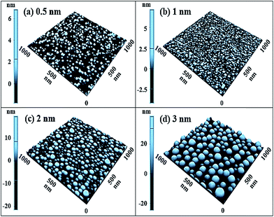
Fig. 2 and 3 show the development of dome shape self-assembled Au NPs on Al2O3 (0001) with the variation of Au deposition amount between 0.5 and 3 nm with fixed annealing temperature and duration at 1000 °C for 450 s. Fig. 2 describes the morphology of Au NPs in terms of AFM top-views, cross-section surface line profiles and FFT power spectra and Fig. 3 presents their corresponding 3-D AFM side-views. In general, the self-assembled dome shaped Au NPs were fabricated on sapphire surface and grew larger in compensation of the decrease in density accordingly with the increased Au deposition amount up to 3 nm. The shape of Au NPs can be the influence of various factors such as diffusion length, surface energy, deposition amount, size, atomic structure of substrates. In our case, we systematically varied the Au deposition amount on sapphire so that the size of fabricated Au NPs also increase resulting in the changes in surface energy as a results the shape of the Au NPs also changes accordingly. With the sufficient thermal energy at 1000 °C, the surface diffusion is also expected to be sufficient for the fabrication of 3-D Au NPs according to the Volmer–Weber growth model. The binding energy between Au adatoms (EA) can be higher than the Au adatoms and sapphire surface atoms (ES) such that, the EA > ES leads to the stronger bonding between the Au adatoms, and as a result, the self-assembled Au 3-D NPs can be formed on the surface of sapphire.23,24 Due to the low surface energy of Au NPs fabricated between 0.5 and 3 nm, the shape of Au NPs were dome that reflect the isotropic energy distribution over all directions. Initially, at 0.5 nm of Au deposition, small size and low density Au NPs were fabricated on sapphire as shown in Fig. 2(a) and 3(a). At very low amount of Au deposition, less number (density) of Au NPs were observed which is an exceptional case compared with succeeding samples and this may be due to the insufficient amount of Au on substrates area. With the increased deposition amount double to 1 nm, the densely packed dome shaped Au NPs were observed with the increased size and density as demonstrated by the AFM top-views and side-view in Fig. 2(b) and 3(b). At 2 nm Au deposition, the NPs grew and slightly separated apart whereas the density was decreased as shown in Fig. 2(c) and 3(c). Finally, uniform sized dome-shaped self-assembled Au NPs were observed at 3 nm Au deposition as shown in the Fig. 2(d) and 3(d). The AFM top-view and side-view show the distinct shape, size and density of self-assembled Au NPs and the size was gradually increased while the density was further decreased. The average height, average lateral width and average density of self-assembled Au NPs with 3 nm Au deposition were 47.2 nm, 102.7 nm and 1.02 × 1010 cm−2, respectively as listed in Table S2.† The surface morphology of Au NPs can also be discussed in terms of the cross-sectional line profiles and FFT power spectra. For instance, as shown by the cross-sectional surface line profiles in Fig. 2(a-2)–(d-2), initially the height of Au NPs are short and low density, and with increased Au deposition to 1 nm, the height of NPs was slightly increased, at 2 nm the height further increased with decreased density and eventually large NPs were fabricated with 3 nm of Au deposition. Also, the cross-sectional line profiles showed the dome shape of the particular NPs marked with green lines in AFM top-views. Similarly, the FFT power spectra also reflect the surface morphology of corresponding samples. As clearly shown in Fig. 2(a-3), the FFT power spectra shows the bright round pattern due to the round shape of Au NPs. The wide range height distribution of NPs result the larger and brighter FFT power spectrum in Fig. 2(b-3) compared with the preceding sample. Furthermore, due to the improvement in uniformity of Au NPs, the FFT power spectra pattern became smaller and dimer, as shown in Fig. 2(c), (d) and (c-2). To support the above results, the diffusion length can be obtained from the following equation, LD = √(Dst) where Ds is the surface diffusion coefficient and t is the time between pulses. The surface diffusion coefficient is the function of annealing temperature as known from the scaling relation of Ds ∝ exp(−En/KTa) where En is the diffusion barrier, K is the Boltzmann constant and Ta is the annealing temperature.25 As the annealing temperature is high, the diffusion coefficient is expected to be high and vice versa. In this research, we have identical annealing temperature (1000 °C) for all samples, so the diffusion length also can be sufficient and similar for every growth. Thus, with the addition of Au deposition amount, the NPs absorb more Au adatoms as well as they can attract nearby small NPs due to the lower surface energy of large Au NPs. As a result, small NPs migrated towards the large NPs and aggregate until they reach in equilibrium. Thus, the size of NPs increased as a compensation of density with increased deposition amount. Thereby, as shown in Fig. 2(b)–(d) and 3(b)–(d), the size of Au NPs grew larger whereas number of NPs was dropped. Also, the size and density evolution of Au NPs with the incremental variation of deposition amount was studied on GaAs, Si and TiO2 substrates.26–29 Similarly, the Pt NPs on Si and SiO2 substrates,30,31 and Ga NPs on GaAs substrate etc.32 demonstrated the increased dimension as well as decreased density of NPs with the increased deposition amount.
 |
| | Fig. 2 Dome shaped self-assembled Au NPs on Al2O3 with the increased Au deposition amount between 0.5 and 3 nm annealed at 1000 °C for 450 s. (a–d) AFM top views of 3 × 3 μm2. (a-1)–(d-1) AFM top views of 1 × 1 μm2. (a-2)–(d-2) Cross-sectional surface line profiles acquired from the green lines. (a-3)–(d-3) Fourier filter transform (FFT) power spectra. | |
 |
| | Fig. 3 AFM side-views of dome-shaped Au NPs fabricated on sapphire with the variation of deposition amount between 0.5 and 3 nm. (a–d) AFM side views of 1 × 1 μm2. | |
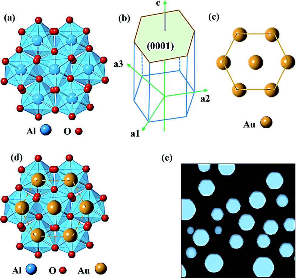
Fig. 4 shows the crystal structure of sapphire (0001), hexagonal representation of (0001) plane, crystal structure of Au (111), crystal structure of Au deposited on sapphire and hexagonal self-assembled Au NPs fabricated on sapphire (0001). The blue sphere represents aluminum (Al), red sphere represents oxygen (O) and the blue shadowing shows the octahedral orientation of Al. Sapphire has a trigonal crystal symmetry where oxygen atoms form hexagonal lattice. The crystal structure of sapphire (0001) is formed by Al3+ and O2− ions with Al3+ cations formed occupying 2/3 of the octahedral sites and O2− anions organized in a hexagonal close packed structure. As shown in Fig. 4(a), the unit structure of hexagonal crystal structure is surrounded by other six hexagonal crystal structure and overall, the arrangement of Al also shows the hexagonal structure. The crystal structure of Au (111) is also hexagonal in Fig. 4(c). We can say that the deposited Au films on the sapphire (0001) after the annealing, the diffused Au adatoms will be positioned on Al accordingly with the hexagonal arrangement of Al and crystal structure of Au (111), as shown in Fig. 4(d). Thus, the influence of hexagonal crystal structure of substrate exhibits the actual morphology of formed nanostructures by the appropriated control of deposition amount and annealing temperature, as clearly seen the hexagonal NPs in Fig. 4(e). This can be evidenced by the previous results in which the fabrication of Au and Cu on sapphire (0001) demonstrate the hexagonal shape NPs with the top terminated (111) plane parallel to the base plane (0001) of sapphire.33,34
 |
| | Fig. 4 (a) Crystal structure of Al2O3 (0001), where the blue balls denotes aluminum and red balls denotes oxygen. (b) An illustration of a hexagonal (0001) plane. (c) Crystal structure of Au (111). (d) Crystal structure after Au deposition on Al2O3 (0001) and Au atoms sit on top of Al atoms. (e) Atomic force microscopy top view of hexagonal self-assembled Au NPs fabricated on Al2O3 (0001) with 4 nm of Au deposition after annealing at 1000 °C for 450 s. | |
Fig. 5 shows the truncated hexagonal pyramid shape self-assembled Au NPs on Al2O3 with Au thickness of 4, 24 and 55 nm at 1000 °C of annealing for 450 s. Generally, with increased Au deposition amount, the shape of self-assembled Au NPs transformed from the dome shape to the truncate hexagonal shape in Fig. 5(a)–(b) and eventually NPs got elongated in random directions at high deposition amount in Fig. 5(c). As seen from the surface morphology in the Fig. 2, 3 and 5, the increment of deposition amount is the fundamental mechanism for the shape transformation of self-assembled Au NPs on sapphire. The spherical cap on the top of dome shape Au NPs undergo the transformation to the truncation of hexagonal pyramids. Initially, as the deposition amount was increased to 4 nm, the addition of Au deposition lead to the increased in the size of Au NPs resulting in the formation of truncated NPs. When the NPs grew larger i.e. reaches its critical size around 100 nm, they cannot sustain with the spherical shape such that there appears facets on lowest possible energy surfaces to be a thermodynamically stable.35 The energy distribution of NPs will be anisotropic that they reflect variant properties in their various crystalline surface. The surface energy of the different crystalline planes follows in the order of Au (111) < Au (100) < Au (110), thus the Au (111) is the most stable plane.36 Most often the lowest energy facet (111) are clearly observed by the AFM side-views that are parallel to the (0001) plane of sapphire. Although, there are many other lower energy facets seen in AFM side-views in Fig. 5(a-1), only top facet (111) crystalline plane is clearly distinguished by referring the similar results of Au and Cu on sapphire33–37 and Au on graphite38 in previous research. The AFM top-view shows the regular hexagonal shaped NPs and AFM side view shows truncated 3-D view of corresponding NPs in Fig. 5(a) and (a-1). The cross-sectional surface line profile indicated with the green line also evidence the truncated nature of NPs, as mention in Fig. 5(a-2). The average height and average lateral width were increased by 1.71 times to 80.9 nm and 1.46 times to 150.2 nm whereas density was reduced by 5.33 times to 1.91 × 109 cm−2, as plotted in Fig. 6(c)–(e) and listed in Table S2.† With the small increment on deposition amount between 4.25 and 5 nm, the size of truncated hexagonal pyramid NPs increased while the density was decreased, as shown by AFM images, SEM images and plot in the Fig. S5–S7.† When the Au deposition amount was highly increased to 24 nm, the size of NPs increased whereas the shape remains hexagonal truncated, as shown by AFM top and side views in Fig. 5(b) and (b-1). The cross-sectional surface line profile in Fig. 4(b-2) shows the increased dimension and truncated morphology of the self-assembled Au NPs. The hexagonal shape of corresponding sample can be clearly viewed by the SEM image in Fig. 7(a). The average height and lateral width of self-assembled Au NPs were increased by 7.78 times to 630.9 nm and 7.77 times to 1168.2 nm while the density was dropped by 147 times to 1.3 × 107 cm−2, as listed in Table S2† and plotted in Fig. 6(c)–(e). With drastically increase of Au deposition amount to 55 nm, the truncated Au NPs tends to be elongated in random directions as clearly shown by AFM images in Fig. 5(c) and SEM image in Fig. 7(b). Most of the NPs are truncated irregular hexagonal with some of the edge comparatively large, however few regular hexagonal NPs were also observed. The top facet of Au NPs is an irregular hexagonal as clearly shown by the AFM side-view in Fig. 5(c-1) and the truncated nature of NPs is evidenced by the cross-sectional line profile in Fig. 5(c-2). It was observed that with increased Au deposition amount more than 2 times to 55 nm, the average height was approximately increased by 1.19 times and lateral width is increased by 2.17 times whereas average density is decreased by 1.69 times such that average height and lateral width were 751.1 and 2539.8 nm and average density was 1.91 × 106 cm−2 as listed in Table S2† and plotted in Fig. 6(c)–(e).
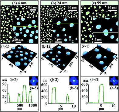 |
| | Fig. 5 Truncated hexagonal pyramid shape self-assembled Au NPs on Al2O3 (0001) with Au thickness of 4, 24 and 55 nm at 1000 °C of annealing for 450 s. (a–c) AFM top views of 3 × 3, 40 × 40, and 40 × 40 μm2 with small scale AFM top view of 1 × 1, 10 × 10, and 10 × 10 μm2, respectively. (a-1)–(c-1) AFM side views of corresponding small scale AFM top views. (a-2)–(c-2) Cross-sectional surface line-profiles acquired from the green lines. (a-3)–(c-3) FFT power spectra. | |
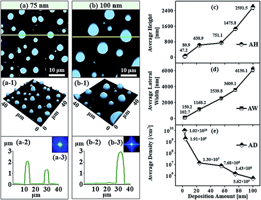 |
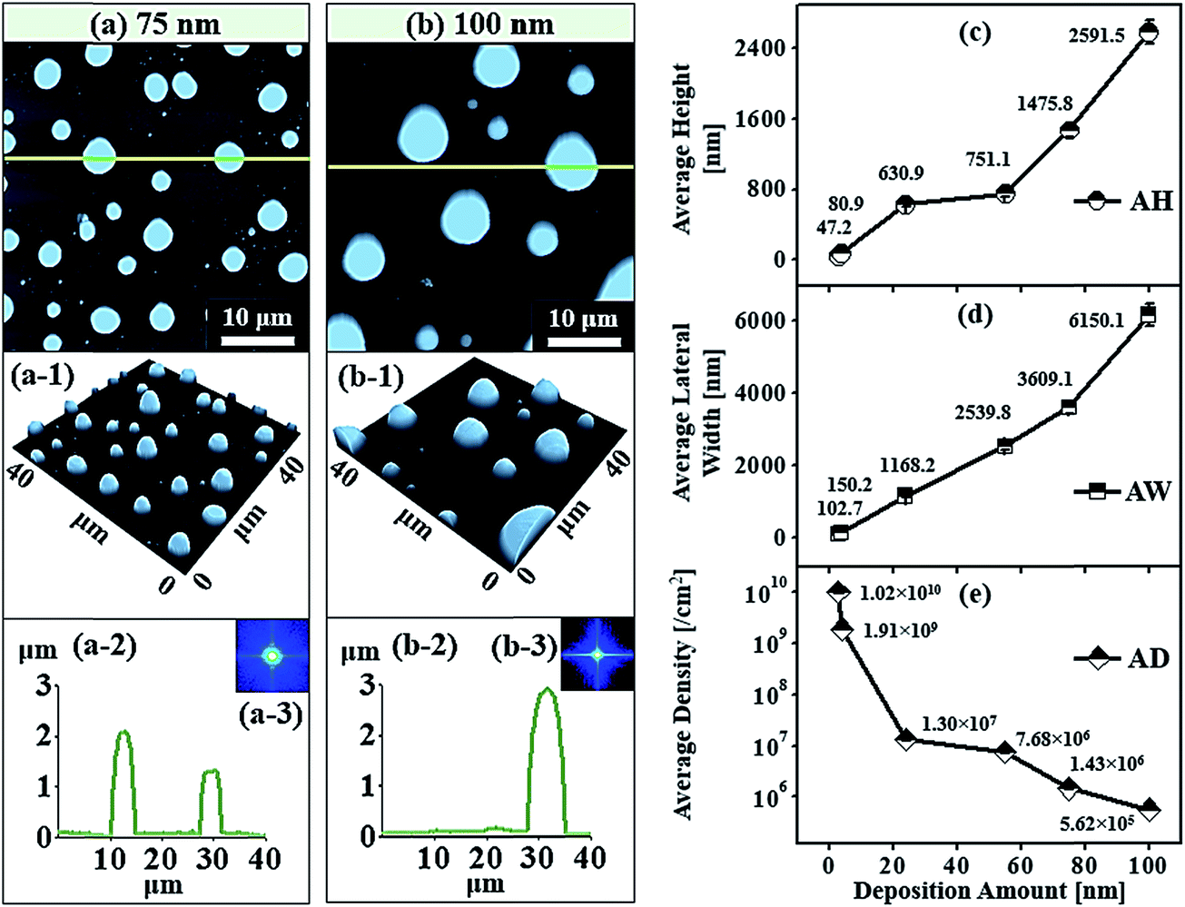
| | Fig. 6 Truncated cone and dome shape self-assembled Au NPs on Al2O3 (0001) by the control of Au deposition amount at 75 and 100 nm at 1000 °C of annealing for 450 s. (a–b) AFM top views of 40 × 40 μm2. (a-1)–(b-1) AFM side views of corresponding samples. (a-2)–(b-2) Cross-sectional surface line-profiles acquired from the green lines. (a-3)–(b-3) FFT power spectra. Plots of (c) average height (AH), (d) average lateral width (AW) and (e) average density (AD) of self-assembled Au NPs with various deposition amount between 3 and 100 nm. Error bars: ± 5%. | |
 |
| | Fig. 7 Scanning electron microscopy (SEM) images of various Au NPs fabricated on Al2O3 (0001) to illustrate the evolution of shape and size of self-assembled Au NPs. (a) Truncated hexagonal pyramid shape Au NPs at 24 nm of Au deposition. (b) Elongated truncated hexagonal pyramid shape Au NPs at 55 nm of Au deposition. (c) Truncated cone shape self-assembled Au NPs at 75 nm of Au deposition. (d) Dome shape self-assembled Au NPs at 100 nm of Au deposition. (a–d) are of 40(x) × 24(y) μm2. (e) SEM image. (e-1) Enlarged view of multifaceted dome Au NP. | |
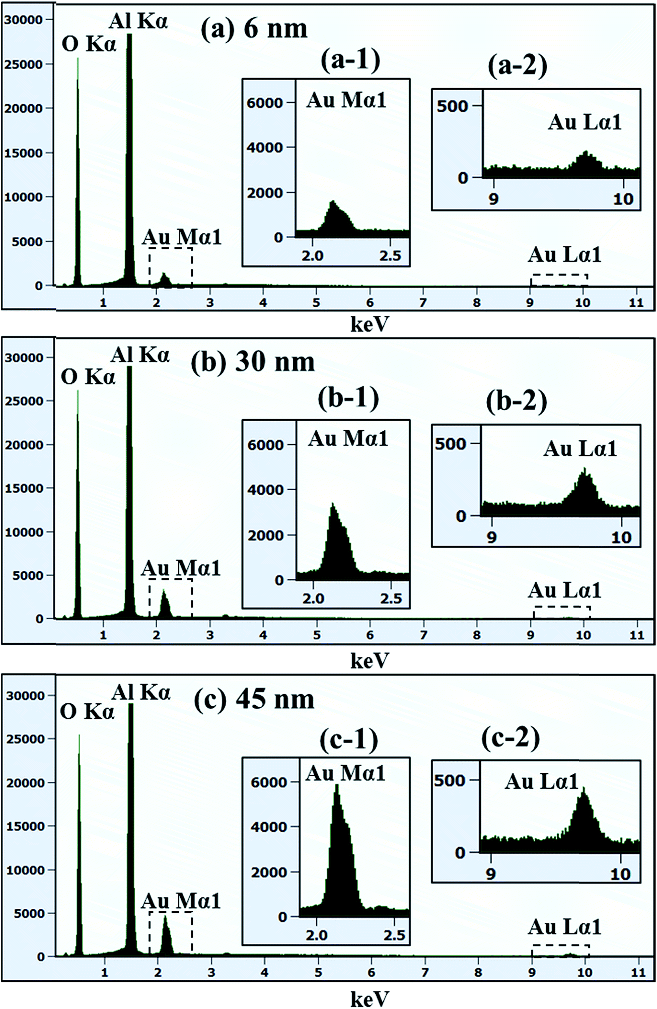
Fig. 6 represents the truncated cone and dome shape self-assembled Au NPs on Al2O3 (0001) with the Au deposition amount 75 and 100 nm at 1000 °C of annealing for 450 s. In general, the size increased and shape transformation and density reduction of self-assembled Au NPs were clearly observed with the increased Au deposition amount from 55 to 75 and 100 nm. The hexagonal shape truncated NPs are transformed to multi-faceted dome shape or truncated cone shape Au NPs with increased Au deposition amount 75 nm, as shown by AFM top-view and side-view in Fig. 6(a) and (a-1). When the height of NPs become very large around 2 μm or more, additional high index crystalline planes or facets appear in NPs resulting in the overall shape of NPs appearing as curve or dome.39,40 The cross-sectional profile line marked with the green line in Fig. 6(a-2) shows the curve and plane at top such that the fabricated NPs are the truncated cone and dome shape. The top-view of truncated cone and dome shaped Au NPs are round in shape which is also evidenced by the SEM image in Fig. 7(c) and S8(a).† The average height of self-assembled Au NPs was increased by 1.96 times to 1475.8 nm and lateral width by 1.42 times to 3609.1 nm but density was dropped by 5.34 times to 1.43 × 106 cm−2. At 100 nm of Au deposition, self-assembled Au NPs with multi-faceted dome shape was observed. The AFM top-view shows round shape and side-view shows the dome shaped self-assembled Au NPs in Fig. 6(b) and (b-1) and the corresponding SEM images are shown in Fig. 7(d), S8(b) and S9.† The cross-sectional surface line profile in Fig. 6(b-2) clearly shows the curve shape of line profile obtained from the green line. The average height and average lateral width were observed as 2591.5 and 6150.1 nm, respectively but the density was reduced to 5.62 × 105 cm−2. The average height was increased by 1.75 times, the average lateral width increased by 1.70 times whereas average density was decreased by 2.55 times compared with the preceding sample. Fig. 8 shows the energy dispersive X-ray spectroscopy (EDS) spectra of various deposition amount of Au on sapphire (0001) annealed at 1000 °C for 450 s. Fig. 8(a)–(c) show the EDS spectra of self-assembled Au NPs fabricated with 6, 30 and 45 nm of Au deposition, respectively. The X-axis of EDS spectra denotes the energy level (keV) and Y-axis represents the count of corresponding energy level. The enlarged peaks of Au Mα1 and Lα1 are shown in the insets of Fig. 8(a-1)–(c-1) and (b-2)–(c-2), in which it is clearly observed, the evolution of Au Mα1 at 2.131 and Au Lα1 peaks at 9.707 keV with the variation of Au deposition amount. For example, the count of Au Mα1 peak at 30 nm deposition is approximately 3700 while that of 6 nm Au deposition showed only ∼1700. Similarly, the count of Au Mα1 peaks reached approximately 6000 with 45 nm Au deposition. Likewise, the count of Au Lα1 peaks increased with increased deposition amount. Overall, an appropriate control of Au deposition amount, the shape of Au NPs can be re-demonstrated such that dome shape self-assembled Au NPs were fabricated in small amount of Au deposition amount between 0.5 and 3 nm as well as at high amount of Au deposition amount of 75 and 100 nm. The transformation of self-assembled Au NPs shape from the dome to the truncated hexagon, elongated truncated hexagon, truncated and dome were demonstrated with systematic control of Au deposition amount between 0.5 and 100 nm at fixed annealing temperature and duration. Similar to our results of shape transformation, the transformation of metal NPs have been studied on various growth mechanism with demonstrating various shape and size of metal NPs.41–43 The Au nanocrystals in the shape of octahedra, truncated octahedra, cuboctahedra, cubes, and higher polygons were observed by increasing the silver nitrate concentration.41 The Au nanostructures with octahedral, rhombic dodecahedra, truncated ditetragonal prisms and concave cubes have been demonstrated by the systematic increment change in the Ag+ concentration in the reaction solution using seed-mediated growth method.42 Furthermore, during annealing an Au film on graphene, the shape of Au NPs transform from hexagonal to triangular with increased the amount of Au thickness.43
 |
| | Fig. 8 Energy dispersive X-ray spectroscopy (EDS) spectra of various deposition amount of Au on Al2O3 (0001) at fixed annealing temperature and duration at 1000 °C for 450 s. (a) 6 nm of Au deposition. (b) 30 nm of Au deposition. (c) 45 nm of Au deposition. (a-1)–(c-1) Enlarged spectra between 2 and 2.5 keV. (a-2)–(c-2) Enlarged spectra between 9 and 10 keV. The Y-axis and X-axis are the count and the energy level, respectively. | |
Conclusions
We have successfully investigated the shape, size and density of self-assembled Au NPs on sapphire (0001) with increasing Au deposition amount. The shape, size and density of self-assembled Au NPs were strongly dependent on the amount of Au deposition. Based on the Volmer–Weber growth model, the Au NPs were successfully formed and depending on the surface free energy distribution in relation to the volume of NPs, the transformation of NP configuration from isotropic to anisotropic and again isotropic (multi-faceted) was observed. With increasing Au deposition amount, the shape of self-assembled Au NPs transformed from the dome to the truncated hexagon, truncated hexagon to truncated cone, and truncated cone to multi-faceted dome and the size of self-assembled Au NPs increased while density decreased. Initially, between 0.5 and 3 nm of Au deposition amount, dome shaped self-assembled Au NPs were fabricated. With increasing Au deposition between 4 and 55 nm, the truncated hexagonal shaped self-assembled Au NPs were demonstrated. With 4 and 24 nm of Au deposition, the shape of self-assembled Au NPs were truncated regular hexagon while the edge of hexagon were irregular at 55 nm such that the NPs edge elongated in one direction. The hexagon shape were transformed to round at 75 nm of Au deposition such that the truncated cone shaped self-assembled Au NPs were fabricated. At 100 nm of Au deposition amount, the self-assembled Au NPs retained its dome shape. Also, the increment in Au deposition amount led to the size increase of NPs whereas the density decrease.
Acknowledgements
Financial support from the National Research Foundation (NRF) of Korea (no. 2011-0030821 and 2013R1A1A1007118), and in part by the research grant of Kwangwoon University in 2015 is gratefully acknowledged. This work was conducted during the sabbatical year of Kwangwoon University in 2015.
Notes and references
- K. L. Kelly, E. Coronado, L. L. Zhao and G. C. Schatz, J. Phys. Chem. B, 2003, 107, 668–677 CrossRef CAS.
- C. N. R. Rao, G. U. Kulkarni, P. J. Thomas and P. P. Edwards, Chem.–Eur. J., 2002, 8, 28–35 CrossRef CAS.
- M. A. El-Sayed, Acc. Chem. Res., 2001, 34, 257–264 CrossRef CAS PubMed.
- S. T. Han, Y. Zhou, Z. X. Xu, V. A. L. Roy and T. F. Hung, J. Mater. Chem., 2011, 21, 14575–14580 RSC.
- D. Huang, F. Liao, S. Molesa, D. Redinger and V. Subramanian, J. Electrochem. Soc., 2003, 150, G412–G417 CrossRef CAS PubMed.
- T. H. Meen, J. K. Tsai, S. M. Chao, Y. C. Lin, T. C. Wu, T. Y. Chang, L. W. Ji, W. R. Chen, I. T. Tang and C. J. Huang, Nanoscale Res. Lett., 2013, 8, 1–6 CrossRef PubMed.
- S. S. Shankar, A. Rai, A. Ahmad and M. Sastry, Chem. Mater., 2005, 17, 566–572 CrossRef CAS.
- A. I. Kuznetsov, A. B. Evlyukhin, M. R. Gonçalves, C. Reinhardt, A. Koroleva, M. L. Arnedillo, R. KIyan, O. Marti and B. N. Chichkov, ACS Nano, 2011, 5, 4843–4849 CrossRef CAS PubMed.
- P. K. Jain, K. S. Lee, I. H. El-Sayed and M. A. El-Sayed, J. Phys. Chem. B, 2006, 110, 7238–7248 CrossRef CAS PubMed.
- R. Narayanan and M. A. El-Sayed, Langmuir, 2005, 21, 2027–2033 CrossRef CAS PubMed.
- M. C. Daniel and D. Astruc, Chem. Rev., 2004, 104, 293–346 CrossRef CAS PubMed.
- H. U. I. Zhang, M. Jin, Y. Xiong, B. Lim and Y. Xia, Acc. Chem. Res., 2012, 46, 1783–1794 CrossRef PubMed.
- Y. Sun and Y. Xia, Science, 2002, 298, 2176–2179 CrossRef CAS PubMed.
- J. S. Bradley, B. Tesche, W. Busser, M. Maase and M. T. Reetz, J. Am. Chem. Soc., 2000, 122, 4631–4636 CrossRef CAS.
- M. Y. Li, M. Sui, E. S. Kim and J. Lee, Nanoscale Res. Lett., 2014, 9, 1–10 CrossRef PubMed.
- B. J. Wiley, Y. Xiong, Z. Y. Li, Y. Yin and Y. Xia, Nano Lett., 2006, 6, 765–768 CrossRef CAS PubMed.
- C. Li, K. L. Shuford, Q. Park, W. Cai, Y. Li, E. J. Lee and S. O. Cho, Angew. Chem., 2007, 119, 3328–3332 CrossRef PubMed.
- R. Jin, Y. Cao, C. A. Mirkin, K. L. Kelly, G. C. Schatz and J. G. Zheng, Science, 2001, 294, 1901–1903 CrossRef CAS PubMed.
- Y. Yu, Q. Zhang, X. Lu and J. Y. Lee, J. Phys. Chem. C, 2010, 114, 11119–11126 CAS.
- O. Malyi and E. Rabkin, Acta Mater., 2012, 60, 261–268 CrossRef CAS PubMed.
- P. W. Voorhees, J. Stat. Phys., 1985, 38, 231–252 CrossRef.
- J. H. Yao, K. R. Elder, H. Guo and M. Grant, Phys. Rev. B: Condens. Matter Mater. Phys., 1993, 47, 14110 CrossRef.
- J. A. Venables, G. D. T. Spiller and M. Hanbucken, Rep. Prog. Phys., 1984, 47, 399–459 CrossRef.
- D. B. Abraham and C. M. Newman, EPL, 2009, 86, 16002 CrossRef.
- H. Zhou, C. Qiu, Z. Liu, H. Yang, L. Hu, J. Liu, H. Yang, C. Gu and L. Sun, J. Am. Chem. Soc., 2010, 132, 944–946 CrossRef CAS PubMed.
- M. Y. Li, M. Sui, E. S. Kim and J. Lee, Nanoscale Res. Lett., 2014, 9, 1–11 CrossRef PubMed.
- M. Y. Li, M. Sui, E. S. Kim and J. Lee, Cryst. Growth Des., 2014, 14, 1128–1134 CAS.
- M. Sui, M. Y. Li, E. S. Kim and J. Lee, J. Appl. Crystallogr., 2014, 47, 505–510 CrossRef CAS.
- L. Zhang, F. Cosandey, R. Persaud and T. E. Madey, Surf. Sci., 1999, 439, 73–85 CrossRef CAS.
- S. Strobel, C. Kirkendall, J. B. Chang and K. K. Berggren, Nanotechnology, 2010, 21, 505301 CrossRef PubMed.
- J. M. Lee and B. I. Kim, Mater. Sci. Eng., A, 2007, 449, 769–773 CrossRef PubMed.
- D. M. Nothern and J. M. Millunchick, J. Vac. Sci. Technol., B, 2012, 30, 060603 Search PubMed.
- H. Sadan and W. D. Kaplan, J. Mater. Sci., 2006, 41, 5099–5107 CrossRef CAS.
- M. C. R. Jensen, K. Venkataramani, S. Helveg, B. S. Clausen, M. Reichling, F. Besenbacher and J. V. Lauritsen, J. Phys. Chem. C, 2008, 112, 16953–16960 CAS.
- H. P. Bonzel, Phys. Rep., 2003, 385, 1–67 CrossRef CAS.
- P. Wu, H. M. Jin and H. L. Liu, J. Mater. Sci., 2003, 38, 1727–1729 CrossRef CAS.
- T. Worren, K. H. Hansen, E. Lægsgaard, F. Besenbacher and I. Stensgaard, Surf. Sci., 2001, 477, 8–16 CrossRef CAS.
- T. Irawan, I. Barke and H. Hövel, Appl. Phys. A, 2005, 80, 929–935 CrossRef CAS.
- G. Medeiros-Ribeiro, A. M. Bratkovski, T. I. Kamins, D. A. Ohlberg and R. S. Williams, Science, 1998, 279, 353–355 CrossRef CAS.
- C. R. Li, N. P. Lu, J. Mei, W. J. Dong, Y. Y. Zheng, L. Gao, K. Tsukamoto and Z. X. Cao, J. Cryst. Growth, 2011, 314, 324–330 CrossRef CAS PubMed.
- D. Seo, J. C. Park and H. Song, J. Am. Chem. Soc., 2006, 128, 14863–14870 CrossRef CAS PubMed.
- M. L. Personick, M. R. Langille, J. Zhang and C. A. Mirkin, Nano Lett., 2011, 11, 3394–3398 CrossRef CAS PubMed.
- H. Zhou, F. Yu, M. Chen, C. Qiu, H. Yang, G. Wang and L. Sun, Carbon, 2013, 52, 379–387 CrossRef CAS PubMed.
Footnote |
| † Electronic supplementary information (ESI) available. See DOI: 10.1039/c5ra07631e |
|
| This journal is © The Royal Society of Chemistry 2015 |
Click here to see how this site uses Cookies. View our privacy policy here.