
 Open Access Article
 This Open Access Article is licensed under a Creative Commons Attribution-Non Commercial 3.0 Unported Licence
Flexible and in situ fabrication of nanochannels with high aspect ratios and nanopillar arrays in fused silica substrates utilizing focused ion beam†
Yan Xu* and
Nobuhiro Matsumoto
Nanoscience and Nanotechnology Research Center, Research Organization for the 21st Century, Osaka Prefecture University, 1-2, Gakuen-cho, Naka-ku, Sakai, Osaka 599-8570, Japan. E-mail: y-xu@21c.osakafu-u.ac.jp; Fax: +81-72-254-7813; Tel: +81-72-254-7813
First published on 25th May 2015
Abstract
Nanochannels fabricated in fused silica substrates are ideal tools for single (bio)molecular studies in biology and are promising in the development of innovative applications in chemistry. To obtain a higher throughput and a higher level of integration and functionalization, nanochannels with high aspect ratios and nano-in-nano structures are very much desired, but their fabrication is a challenge. Herein, we report a method for fabricating nanochannels with such challenging critical dimensions and structures in fused silica substrates by using a focused ion beam.
Nanofluidic devices, which are microchips incorporating nanometer-scale channels (i.e., nanochannels), are ideal tools to understand behaviors and phenomena of liquids and (bio)molecules confined in stringent nanospaces.1–4 For example, confining a liquid in a nanochannel shows promise in approaching an ultimate goal to precisely handle and characterize single molecules.5–7 Instead of measuring averaged behavior of ensemble molecules, such single molecular approaches are promising for gaining an insight into fundamental phenomena. In addition, recent studies revealed altered properties of water confined in a nanochannel, with higher viscosity,8,9 higher proton mobility,10,11 and lower dielectric constant8 than in the bulk. Such unique properties are very promising to eventually bring epoch-making applications. These applications may include, for example, the realization of ultra-fast chemical reactors, ultra-high-efficiency energy converters, and ultra-high-sensitive analytical devices. Nevertheless, despite the increased exciting progress, the field of nanofluidics is still nascent, in contrast to its thriving ‘brother’ microfluidics. One critical reason is that the capability of excellent control of the geometry of nanochannels is still lacking.
Nanochannels are the ‘hearts’ of nanofluidic devices and their fabrication varies depending on the materials. In the early days of development, nanochannels were fabricated on semiconductor wafers such as silicon, by directly transferring the well-established nanofabrication experience accumulated in microelectronics over several decades.12–14 In the past few years, the fabrication of nanochannels in fused silica substrates was achieved, using several tools as described later. After that, insulating fused silica immediately replaced semiconducting silicon as a major substrate material for fabrication of nanofluidic devices, in addition to a few polymeric substrates15–17 to a lesser extent. Fused silica is a glass consisting of silica in amorphous form. Fused silica possesses excellent properties such as superior optical transparency, chemical/biological inertness, thermal stability, and mechanical robustness. Furthermore, owing to their hydrophilic nature and well-established surface chemistry through a variety of silanization processes, fused silica nanochannels make it easy to perform liquid introduction and inner wall surface modification. These excellent properties are ideal and indispensable for chemical and biological studies, as well as applications at the nanoscale or single-molecular level under nanofluidic conditions.
Several tools have enabled the fabrication of nanochannels in fused silica substrates, with low aspect ratios (depths/widths) or unity (i.e., close to 1) aspect ratios. Standard photolithography incorporated with short-time wet or dry etching allows fabricating fused silica nanochannels with micrometer-scale widths and nanometer-scale depths, defined by the practical resolution limits of photolithography and duration of etching, respectively.18–20 Such nanochannels with low aspect ratios are also called planar nanochannels and have been used in early studies of DNA extension. Electron beam lithography (EBL) coupled with dry etching allows fabricating fused silica nanochannels with unity aspect ratios, namely, square nanochannels.21–24 The dimensions (i.e., widths and depths) of the square nanochannels fabricated by this method usually range from tens to hundreds of nanometers. This range is critically important for studies in nanofluidics because continuum assumptions for the Navier–Stokes (NS) equations,25 which are governing equations in fluid mechanics, still apply. The use of square nanochannels with dimensions in this important range has accelerated studies in nanofluidics, giving birth to the aforementioned discoveries of altered properties of water confined in nanospaces. More recently, an interesting study using sub-5 nm square nanochannels fabricated by focused ion beam (FIB) has extended the possibility of nanochannels to ultimate dimensions below 5 nm,26 where the NS equations no longer apply and liquids can be no longer defined as fluids.
In comparison with low-aspect-ratio planar nanochannels and near-unity-aspect-ratio square nanochannels, high-aspect-ratio nanochannels offer advantages including a higher throughput and a higher level of integration, but their fabrication is even more challenging. Only a few groups have reported the fabrication of high-aspect-ratio nanochannels in silicon27,28 and polymeric substrates,15 using interferometric lithography, proton beam lithography, and others. Nevertheless, the fabrication of high-aspect-ratio nanochannels in fused silica substrates is still a remaining challenge.
In addition, the capability of further defining nanometer-scale geometries inside nanochannels, namely, nano-in-nano structures, promises to bring about more powerful nanochannels with versatile integrated functions. Nanochannels with flat geometries have been widely used to date in a variety of fundamental phenomenon studies. In order to obtain deeper insights into those fundamental phenomena at a more precise level and fully utilize those new findings to develop the aforementioned epoch-making applications, nano-in-nano structures are desired. However, the fabrication of nano-in-nano structured nanochannels in fused silica substrates by using EBL coupled with dry etching needs a super-high-precision alignment technique during multiple-step nanofabrication,29 which unfortunately is a great hurdle.
Herein, we report a method for the fabrication of nanochannels with high aspect ratios and nanochannels with nanopillar arrays in fused silica substrates by utilizing FIB (Fig. 1). FIB has been much employed in the field of semiconductors for milling, deposition, and imaging of semiconducting materials but has seldom been applied to insulating materials.26,30 Our method enables the flexible and in situ fabrication of challenging nanochannel structures in insulating fused silica substrates through a conducting layer (100 nm thick gold layer) pre-deposited on the substrate, under optimized conditions of beam parameters and processing parameters of FIB milling. The gold layer provides capabilities of (1) efficiently allowing sufficient conductance of charge during deep milling of the insulating fused silica substrate, (2) precisely defining the narrow channel feature to get a high aspect ratio, and (3) adequately protecting the surface of the substrate and/or the nanochannel in the case of nano-in-nano fabrication from material redeposition during FIB milling. In addition, the milling guided by simultaneous high-resolution FIB imaging allows positioning of target regions precisely. The high-precision positioning thereby enables the flexible and in situ fabrication of nano-in-nano structures such as nanopillar array nanochannels, without the need to additionally develop a high-precision alignment technique, which is very challenging. We believe that the fabrication method will contribute to the development of nanofluidic devices with a higher throughput and a higher level of integration and functionalization.
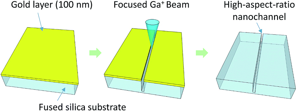 | ||
| Fig. 1 Schematic diagram of the FIB milling process for the fabrication of high-aspect-ratio nanochannels. | ||
It is problematic to directly mill (or sputter) a fused silica substrate by using FIB, due to the charging effect caused by ion irradiation on the insulating substrate. In general, the charging effect arises from accumulation of static electric charges on the surface of a sample. In this study, gallium ion (Ga+) beams (Table 1) were used as ion beam sources. The irradiation of the insulating fused silica with Ga+ ions will bring about the accumulation of excess positive charge on the surface. The charging effect adversely affects the quality of FIB milling, resulting in irregular milled features. We used a gold layer pre-deposited on the fused silica substrate as a conducting layer to overcome these charging problems. As one of the most sensitive materials for FIB milling processes, gold has a significantly high ion milling (or sputtering) yield (15.7 atoms/ion for 40 keV Ga+ ions at normal incidence).31 The high milling yield offers a fast etching rate for the gold layer during FIB milling. In addition, focused Ga+ ion beams are very suitable for milling gold and capable of milling features with vertical slope profiles in the gold layers.32 The fast etching rate together with the vertical etching profile thereby enabled quick transfer of a designed pattern feature (i.e., acting as a mask) to the fused silica layer, with high accuracy. This quickly formed gold mask then played a critical role in maintaining efficient conductance of charge for the Ga+ ion beam to sufficiently mill the fused silica surface. In addition, the conducting gold layer could be easily removed by using a routine chemical etchant. After gold removal, a standard nanofluidic device could be obtained by bonding the substrate containing the FIB-milled nanochannel structures and a substrate containing photolithographically fabricated microchannels through conventional fused silica bonding methods.3,33
| Beam no. | Aperture size (μm) | Beam diameter (nm) | Beam current (nA) | Current density (A cm−2) |
|---|---|---|---|---|
| 1 | 80 | 100 | 0.60 | 7.64 |
| 2 | 40 | 48 | 0.13 | 7.18 |
| 3 | 20 | 24 | 0.02 | 4.42 |
Gold layers with different thickness were tested. A gold layer 100 nm thick was utilized in this study, decided by the milling capability and reproducibility. To verify the capability of milling, the fabrication of nanochannels with large critical dimensions (500 nm in width) was performed under routine FIB milling conditions (40 keV accelerating voltage, 40 μm aperture, 48 nm beam diameter, 0.13 nA beam current). Here, 40 keV is a standard accelerating voltage generally used in the FIB milling mode. The beams were scanned over designed rectangular pattern regions with widths of 500 nm, which were equal to the desired nanochannel widths. Owing to the assistance of the conducting gold layer, nanochannels approximately 500 nm wide were obtained as desired, with varying depths dependent on dwell times (Fig. 2). Here, the dwell time is a critical processing parameter capable of controlling FIB milling. During FIB milling, the FIB spot with a certain diameter (i.e., beam diameter) raster scans the sample surface within the region of a designed graphical pattern. The pattern is composed of graphical pixels that specify the location of the beam spot. The dwell time (typically μs to ms) defines the beam spot irradiation time at each pixel. As shown in Fig. 2, the depths of the milled nanochannels increase with an increase of dwell time, indicating that a longer dwell time could improve milling yields in the vertical direction in the fused silica layer.
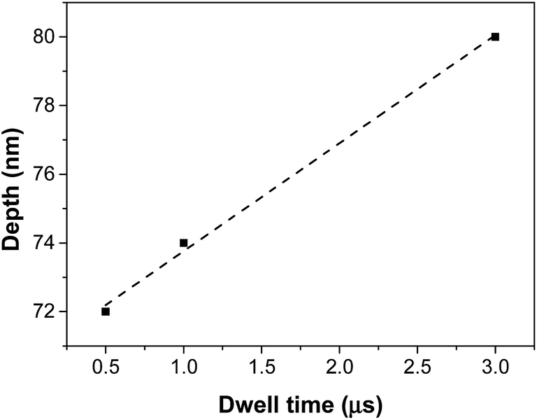 | ||
| Fig. 2 The depth of the FIB-milled nanochannel as a function of the dwell time for the fabrication of nanochannels with large critical dimensions (design width = 500 nm and setting depth = 100 nm) in fused silica substrates under routine FIB milling conditions (40 keV focused Ga+ beam with a beam diameter of 48 nm and a beam current of 0.13 nA). | ||
In addition to dwell time, ion beam parameters such as aperture size, beam diameter, beam current, and current density were further verified and optimized for the fabrication of high-aspect-ratio nanochannels in fused silica substrates. The beam current (typically pA to nA) is directly determined by aperture size (μm) and condenser lens in the optical system of FIB. The current density (A cm−2) correlates with the beam diameter (nm) and the beam current. The values of the corresponding beam parameters of 40 keV Ga+ beams utilized in this study are listed in Table 1. In this experiment, we designed the widths of rectangular patterns to be 100 nm and set the depths for milling to be 600 nm (i.e., 500 nm for the fused silica layer), to obtain 100 nm wide and 500 nm deep fused silica nanochannels after removing the 100 nm gold layer. The setting depth is a processing parameter which can control the amount of milling. For a given setting depth, the number of beam scans over a pattern is directly dependent on the dwell time and the fabrication constant (μm3 nA−1 s−1), which describes the FIB milling efficiency in a certain material. In the case where the fabrication constant of materials is well established, for example silicon, theoretically the actual depth of milling should be approximately equal to the setting depth. However, for the gold/fused silica two-layer system, the fabrication constant is difficult to determine. To make things simpler, in this study we assumed the fabrication constant to be 0.28 μm3 nA−1 s−1, which is equal to that of silicon for 40 keV Ga+ ion beam milling. It should be noted that the actual fabrication constant of the gold/fused silica system may not be 0.28 μm3 nA−1 s−1. By using the assumed fabrication constant, the actual depth becomes only dependent on the dwell time in a given beam condition.
Fig. 3 shows the result of the optimization of the beam diameter and the dwell time for milling of desired high-aspect-ratio nanochannels (100 nm in width, 500 nm in depth, aspect ratio = 5.0). In Fig. 3, width (actual)/width (design) represents the ratio between the actual width and the design width (100 nm), depth (actual)/depth (setting) represents the ratio between the actual depth and the setting depth (500 nm), in the fused silica layer. In the case where both these ratios are near 1.0, the nanochannels as prescribed are considered to be obtained. The widths of the milled nanochannels were dependent on both the beam diameter and the dwell time. The larger the beam diameter, the wider was the milled nanochannel (Fig. 3a). Among the three beam conditions utilized in this study (Table 1), the ion beam with the smallest beam diameter (24 nm; beam 3 in Table 1) enabled milling of the nanochannels with actual widths closest to 100 nm, at each dwell time (0.5 s, 10 s, and 100 s). For the ion beam with a diameter of 24 nm, increasing the dwell time resulted in an increase of the actual depth (Fig. 3b) and thereby an increase of the aspect ratio (Fig. 3c). Nanochannels with high aspect ratios ranging from ca. 3.0 to 5.0 were obtained by using ion beams with a diameter of 24 nm (Fig. 3c). Moreover, at the dwell time of 100 μs in this case, both the ratio of width (actual)/width (design) and the ratio of depth (actual)/depth (setting) were approximately equal to 1 (Fig. 3a and b). These results revealed that the conditions of 40 keV Ga+ ion beam, 24 nm beam diameter, 100 μs dwell time were optimal FIB milling conditions to obtain nanochannels as prescribed for the gold/fused silica system, using the assumed fabrication constant (0.28 μm3 nA−1 s−1).
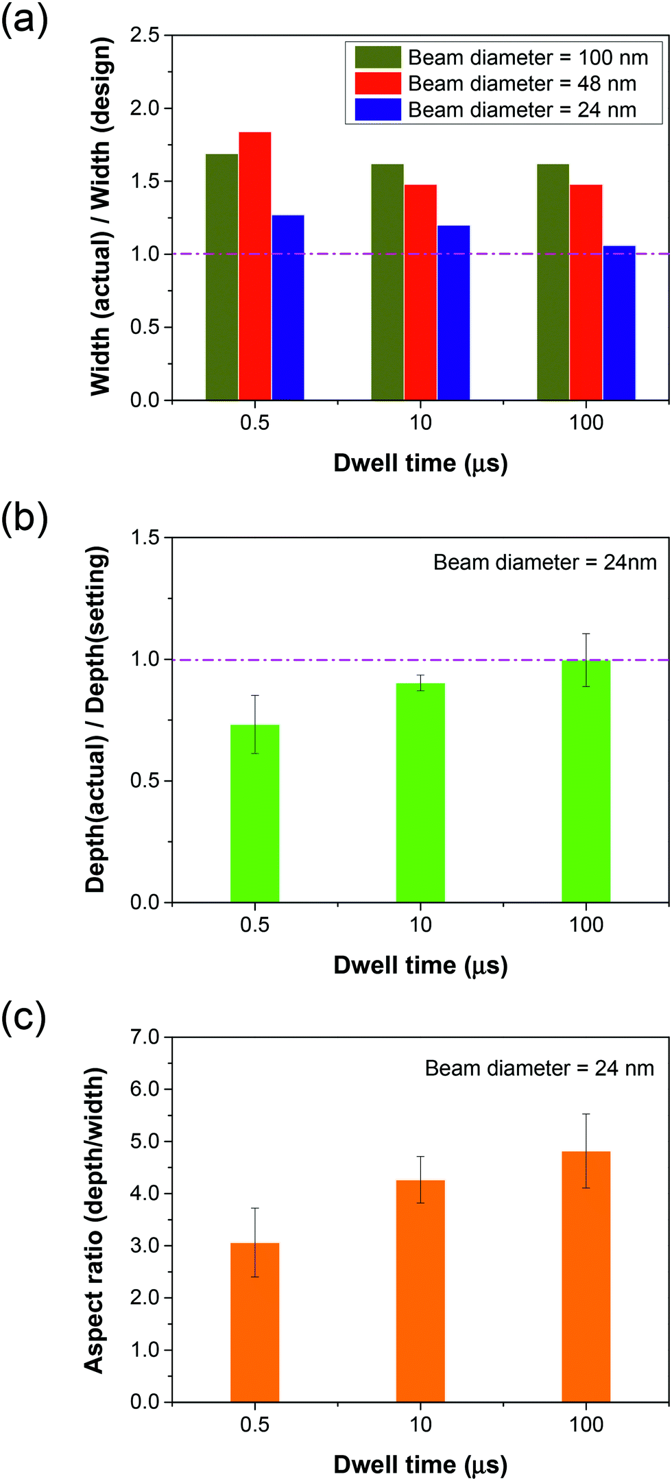 | ||
| Fig. 3 Optimization of the beam diameter and the dwell time for milling high-aspect-ratio nanochannels (design width = 100 nm and setting depth = 500 nm) in fused silica substrates. (a) Width (actual)/width (design) of the nanochannels fabricated using 40 keV Ga+ ion beams with different beam diameters at varying dwell times. (b) Depth (actual)/depth (setting) and (c) aspect ratios (depths/widths) of the nanochannels fabricated using the ion beam with a beam diameter of 24 nm at varying dwell times. Data are mean ± SD, n ≥ 3. | ||
Fig. 4 shows atomic force microscopy (AFM) images and scanning ion microscope (SIM) images for a nanochannel ca. 500 nm deep and ca. 100 nm wide (Fig. 4a and b) and a nanochannel ca. 500 nm deep and ca. 500 nm wide (Fig. 4c and d) which were fabricated using the optimal conditions. While both the width and the depth of the wide nanochannel (500 nm deep and 500 nm wide) could be roughly characterized from its AFM image (Fig. 4c), the depth of the narrow nanochannel (500 nm deep and 100 nm wide) was difficult to determine only from its AFM image (Fig. 4a), due to the larger size (several tens of micrometers) of the cantilever of the AFM than that of the nanochannel. In addition, it was also difficult to obtain the cross-sectional shapes of the nanochannels using the AFM for the same reason. The SIM was used to characterize the cross-sectional shapes of the nanochannels. The SIM images were obtained using an observation mode of our FIB system. An extremely small beam current, lower than 0.01 nA, was used for the SIM observation to avoid damage to the surface of the specimens resulting from ion beam scanning. The cross-sectional shapes of the nanochannels (Fig. 4b and d) were obtained from the observation of the FIB-milled cross-sections tilted 60° with respect to the ion beam. The SIM images revealed that the side walls of both nanochannels were near vertical (5–7°). While the 500 nm deep and 100 nm wide nanochannel had a roughly square cross-section, the 500 nm deep and 500 nm wide nanochannel exhibited a quite sharp bottom due to narrowing of the channel.
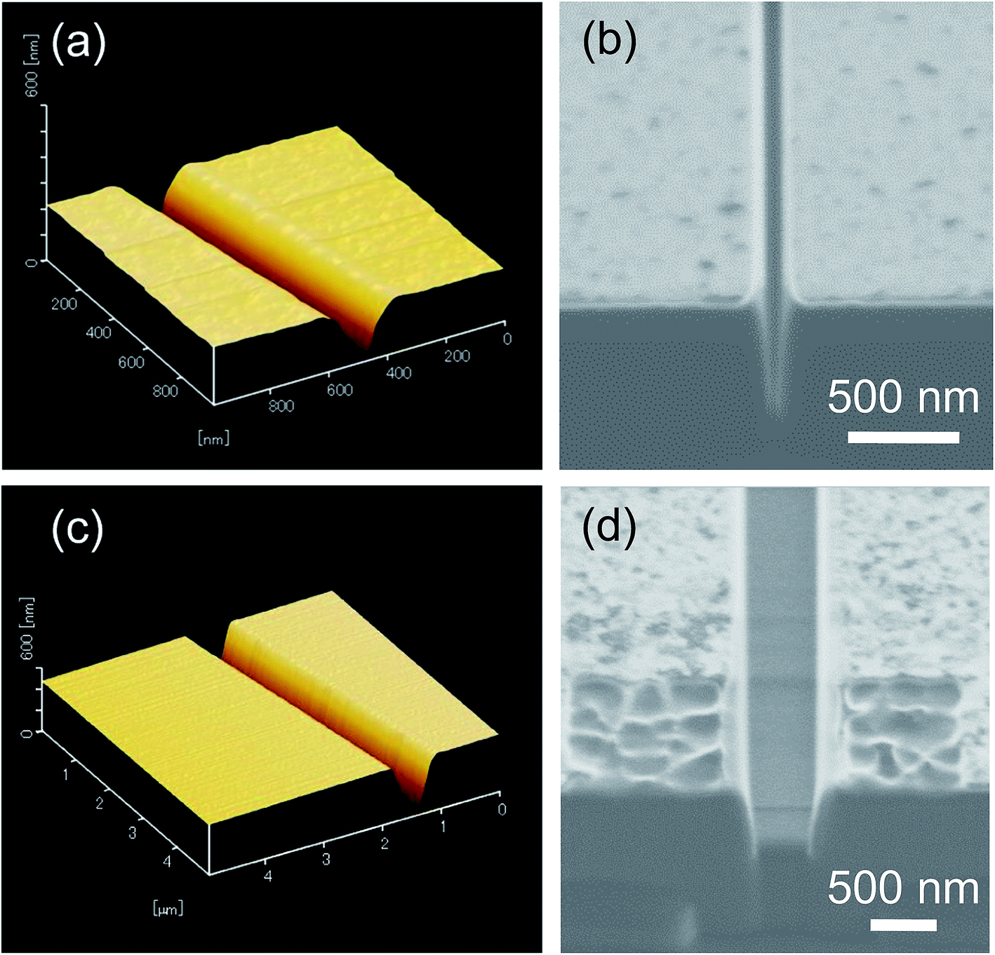 | ||
| Fig. 4 AFM images and SIM images for (a and b) a nanochannel ca. 500 nm deep and ca. 100 nm wide and (c and d) a nanochannel ca. 500 nm deep and ca. 500 nm wide, which were fabricated using the optimal conditions. For (b and d) SIM images, FIB-milled cross-sections of nanochannels were tilted 60° with respect to the ion beam. Note: the bumps on the surface near the cross-section shown in (d) resulted from the FIB milling for obtaining the cross-section of the nanochannel. | ||
Furthermore, the optimal beam conditions (40 keV Ga+ ion beam, 24 nm beam diameter, and 100 μs dwell time) were applied to fabricate nanochannels with nanopillar arrays (Fig. 5). The structures are nano-in-nano structures which are difficult to fabricate with current popular nanochannel fabrication tools for the reason mentioned above. In addition, while microchannels with nanopillars have been reported to possess improved bioseparation capabilities in comparison with microchannels without nanopillars,34,35 similar structures in nanochannels are greatly desired to further improve these capabilities at the nanoscale, but their fabrication is a critical issue. The fabrication of nanochannels with nanopillar arrays was achieved through either a flexible one-step FIB milling strategy (Fig. 5a) or an in situ two-step FIB milling strategy (Fig. 5b). For the former (Fig. 5a), the nanochannel and the nanopillars were simultaneously fabricated in a single FIB milling process, and therefore a nanochannel with nanopillars whose heights are approximately equal to the height (i.e., depth) of the nanochannel could be obtained, as shown in Fig. 5c and d. For the latter (Fig. 5b), the nanochannel and the nanopillars were sequentially fabricated through two independent millings in situ, and therefore a nanochannel with nanopillars whose heights are less than the height (i.e., depth) of the nanochannel could be obtained, as shown in Fig. 5e and f. Nanopillars with sizes (widths or diameters) ranging from hundreds (Fig. 5c–e) to tens (Fig. 5f) of nanometers as well as aspect ratios (heights/sizes) varying from 0.9 (Fig. 5e) to 2.5 (Fig. 5c) were successfully fabricated in both planar (Fig. 5c–e) and square (Fig. 5f) nanochannels. The density of the nanopillar array, which is characterized by the ratio of the sizes of nanopillars to the space between nanopillars (width/space, in short), could be flexibly adjusted. For example, Fig. 5c shows a SIM image of a nanochannel with a low-density (size/space of ca. 0.2) nanopillar array, and Fig. 5d–f show SIM images of nanochannels with relatively high-density (width/space of ca. 1.0–1.1) nanopillar arrays. These results revealed that both milling strategies enabled the flexible and in situ fabrication of nanopillar array nanochannels with prescribed sizes, aspect ratios, and densities of the nanopillars, as well as prescribed widths and depths of the nanochannels.
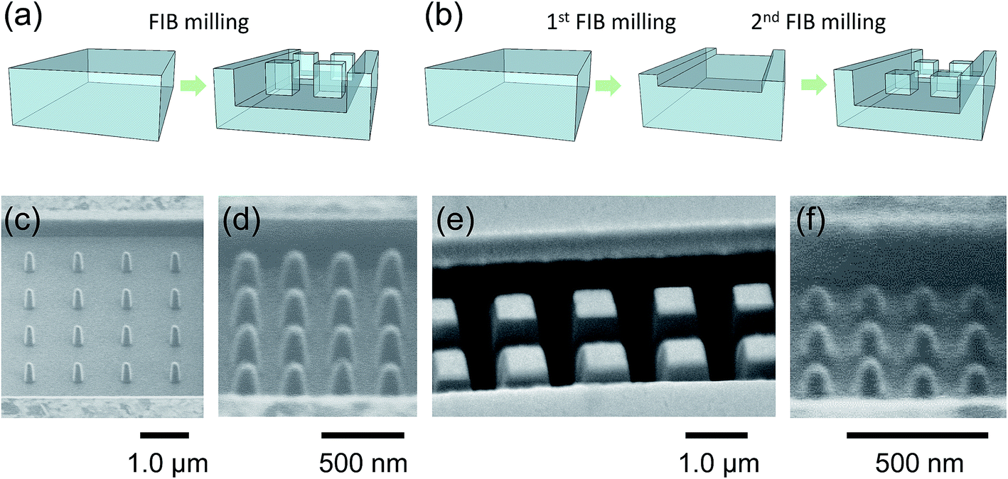 | ||
| Fig. 5 FIB milling strategies (a and b) and SIM images (c–f) of nanochannels with nanopillar arrays. (a) The one-step milling strategy. (b) The two-step milling strategy. (c) A low-density nanopillar (180 nm wide, 450 nm high, aspect ratio = 2.5, spaced by 900 nm) array in a nanochannel with a depth of 450 nm, and (d) a high-density nanopillar (150 nm wide, 320 nm high, aspect ratio = 2.1, spaced by 150 nm) array in a nanochannel with a depth 320 nm, which were fabricated using (a) the one-step FIB milling strategy. (e) A nanopillar (520 nm wide, 480 nm high, aspect ratio = 0.9, spaced by 480 nm) array in a planar nanochannel (700 nm deep and 3 μm wide), and (f) a nanopillar (80 nm wide, 120 nm high, aspect ratio = 1.5, spaced by 120 nm) array in a square nanochannel (400 nm deep, 800 nm wide), which were fabricated using (b) the two-step FIB milling strategy. | ||
In conclusion, we presented a method for fabricating high-aspect-ratio nanochannels as well as nanopillar array nanochannels in fused silica substrates. The method involved FIB milling of nanochannel structures through a 100 nm gold layer pre-deposited on the fused silica substrates, under optimized conditions of beam parameters and processing parameters. The use of a gold layer provided advantages of allowing flexibly and efficiently milling of deep and narrow nanochannels in the insulating fused silica substrates. With the method, the fabrication of nanochannels with high aspect ratios ranging from ca. 3.0 to 5.0 was achieved. Furthermore, in situ fabrication of nanochannels having nanopillar arrays with prescribed sizes ranging from hundreds to tens of nanometers, varying aspect ratios from ca. 0.9 to 2.5, and desired densities in the nanochannels was accomplished. The method would be useful for developing integrated nanofluidic devices with high throughput.
Acknowledgements
This work was partially supported by JSPS KAKENHI grant numbers 26706010, 26630403, MEXT KAKENHI number 26107714, and the Asahi Glass Foundation.Notes and references
- W. Sparreboom, A. van den Berg and J. C. T. Eijkel, Nat. Nanotechnol., 2009, 4, 713–720 CrossRef CAS PubMed.
- A. Piruska, M. Gong, J. V. Sweedler and P. W. Bohn, Chem. Soc. Rev., 2010, 39, 1060–1072 RSC.
- Y. Xu, K. Jang, T. Yamashita, Y. Tanaka, K. Mawatari and T. Kitamori, Anal. Bioanal. Chem., 2012, 402, 99–107 CrossRef CAS PubMed.
- T. Tsukahara, T. Maeda, A. Hibara, K. Mawatari and T. Kitamori, RSC Adv., 2012, 2, 3184–3186 RSC.
- S. L. Levy and H. G. Craighead, Chem. Soc. Rev., 2010, 39, 1133–1152 RSC.
- L. D. Menard, C. E. Mair, M. E. Woodson, J. P. Alarie and J. M. Ramsey, ACS Nano, 2012, 6, 9087–9094 CrossRef CAS PubMed.
- K. Frykholm, M. Alizadehheidari, J. Fritzsche, J. Wigenius, M. Modesti, F. Persson and F. Westerlund, Small, 2014, 10, 884–887 CrossRef CAS PubMed.
- A. Hibara, T. Saito, H. B. Kim, M. Tokeshi, T. Ooi, M. Nakao and T. Kitamori, Anal. Chem., 2002, 74, 6170–6176 CrossRef CAS.
- N. R. Tas, J. Haneveld, H. V. Jansen, M. Elwenspoek and A. van den Berg, Appl. Phys. Lett., 2004, 85, 3274–3276 CrossRef CAS PubMed.
- S. R. Liu, Q. S. Pu, L. Gao, C. Korzeniewski and C. Matzke, Nano Lett., 2005, 5, 1389–1393 CrossRef CAS.
- T. Tsukahara, A. Hibara, Y. Ikeda and T. Kitamori, Angew. Chem., Int. Ed., 2007, 46, 1180–1183 CrossRef CAS PubMed.
- J. Han and H. G. Craighead, J. Vac. Sci. Technol., A, 1999, 17, 2142–2147 CAS.
- J. Haneveld, H. Jansen, E. Berenschot, N. Tas and M. Elwenspoek, J. Micromech. Microeng., 2003, 13, S62–S66 CrossRef CAS.
- J. L. Perry and S. G. Kandlikar, Microfluid. Nanofluid., 2006, 2, 185–193 CrossRef CAS.
- K. A. Mahabadi, I. Rodriguez, S. C. Haur, J. A. van Kan, A. A. Bettiol and F. Watt, J. Micromech. Microeng., 2006, 16, 1170–1180 CrossRef CAS.
- L. H. Thamdrup, A. Klukowska and A. Kristensen, Nanotechnology, 2008, 19, 125301 CrossRef PubMed.
- R. Chantiwas, M. L. Hupert, S. R. Pullagurla, S. Balamurugan, J. Tamarit-Lopez, S. Park, P. Datta, J. Goettert, Y. K. Cho and S. A. Soper, Lab Chip, 2010, 10, 3255–3264 RSC.
- A. Balducci, P. Mao, J. Y. Han and P. S. Doyle, Macromolecules, 2006, 39, 6273–6281 CrossRef CAS.
- J. D. Cross, E. A. Strychalski and H. G. Craighead, J. Appl. Phys., 2007, 102, 024701 CrossRef PubMed.
- G. B. Salieb-Beugelaar, J. Teapal, J. van Nieuwkasteele, D. Wijnperle, J. O. Tegenfeldt, F. Lisdat, A. van den Berg and J. C. T. Eijkel, Nano Lett., 2008, 8, 1785–1790 CrossRef CAS PubMed.
- E. Tamaki, A. Hibara, H. B. Kim, M. Tokeshi, T. Ooi, M. Nakao and T. Kitamori, Anal. Sci., 2006, 22, 529–532 CrossRef CAS.
- W. Reisner, J. P. Beech, N. B. Larsen, H. Flyvbjerg, A. Kristensen and J. O. Tegenfeldt, Phys. Rev. Lett., 2007, 99, 058302 CrossRef.
- M. Graczyk, M. Balaz, A. Kvennefors, H. Linke and I. Maximov, J. Vac. Sci. Technol., B: Nanotechnol. Microelectron.: Mater., Process., Meas., Phenom., 2012, 30, 06FF09 Search PubMed.
- K. Shirai, K. Mawatari and T. Kitamori, Small, 2014, 10, 1514–1522 CrossRef CAS PubMed.
- B. J. Kirby, Micro- and nanoscale fluid mechanics: transport in microfluidic devices, Cambridge University Press, New York, 2010 Search PubMed.
- L. D. Menard and J. M. Ramsey, Nano Lett., 2011, 11, 512–517 CrossRef CAS PubMed.
- M. J. O'Brien, P. Bisong, L. K. Ista, E. M. Rabinovich, A. L. Garcia, S. S. Sibbett, G. P. Lopez and S. R. J. Brueck, J. Vac. Sci. Technol., B: Microelectron. Nanometer Struct.–Process., Meas., Phenom., 2003, 21, 2941–2945 CrossRef.
- A. L. Garcia, L. K. Ista, D. N. Petsev, M. J. O'Brien, P. Bisong, A. A. Mammoli, S. R. J. Brueck and G. P. Lopez, Lab Chip, 2005, 5, 1271–1276 RSC.
- Y. Xu, N. Matsumoto, Q. Wu, Y. Shimatani and H. Kawata, Lab Chip, 2015, 15, 1989–1993 RSC.
- W. X. Li, G. Lalev, S. Dimov, H. Zhao and D. T. Pham, Appl. Surf. Sci., 2007, 253, 3608–3614 CrossRef CAS PubMed.
- P. G. Blauner, J. S. Ro, Y. Butt and J. Melngailis, J. Vac. Sci. Technol., B: Microelectron. Process. Phenom., 1989, 7, 609–617 CAS.
- K. P. Müller, Microelectron. Eng., 1990, 11, 443–447 CrossRef.
- Y. Xu, C. X. Wang, Y. Y. Dong, L. X. Li, K. Jang, K. Mawatari, T. Suga and T. Kitamori, Anal. Bioanal. Chem., 2012, 402, 1011–1018 CrossRef CAS PubMed.
- T. Yasui, N. Kaji, M. R. Mohamadi, Y. Okamoto, M. Tokeshi, Y. Horiike and Y. Baba, ACS Nano, 2011, 5, 7775–7780 CrossRef CAS PubMed.
- T. Yasui, S. Rahong, K. Motoyama, T. Yanagida, Q. Wu, N. Kaji, M. Kanai, K. Doi, K. Nagashima, M. Tokeshi, M. Taniguchi, S. Kawano, T. Kawai and Y. Baba, ACS Nano, 2013, 7, 3029–3035 CrossRef CAS PubMed.
Footnote |
| † Electronic supplementary information (ESI) available: Experimental section. See DOI: 10.1039/c5ra06306j |
| This journal is © The Royal Society of Chemistry 2015 |