
Enhanced thermoelectric performance of layered SnS crystals: the synergetic effect of temperature and carrier concentration†
Bao-Zhen Sunabc,
Zuju Maa,
Chao Hea and
Kechen Wu*a
aState Key Laboratory of Structural Chemistry, Fujian Institute of Research on the Structure of Matter, Chinese Academy of Sciences, Fuzhou 350002, China. E-mail: wkc@fjirsm.ac.cn; Fax: +86 591 83792932; Tel: +86 591 83792600
bSchool of Chemistry and Chemical Engineering, Guangxi University, Nanning 530004, China
cKey Laboratory of Coal to Ethylene Glycol and Its Related Technology, Fujian Institute of Research on the Structure of Matter, Chinese Academy of Sciences, Fuzhou 350002, China
First published on 23rd June 2015
Abstract
We present a detailed theoretical study of the SnS compound, which has not been investigated in depth to date, concerning its crystal structure, electronic structure and thermoelectric property. The results of this study show that pure SnS is not a good thermoelectric material but that its ZT can be increased by adjusting both the temperature and carrier concentration. Further, the optimal temperatures and carrier concentrations for producing the peak ZT are identified. The peak ZT is always below unity in the low-temperature Pnma phase; conversely, when the crystal undergoes a displacive phase transition at 878 K, the peak ZT is enhanced to 1.61 ± 0.02 at 1080 K. Additionally, the average ZT in the Cmcm phase (e.g., approximately 1.3) is significantly higher than that in the Pnma phase (e.g., 0.31 ± 0.05). Therefore, the optimally doped SnS material may be highly efficient in its thermal-to-electrical energy conversion at high temperatures. We attribute the remarkable high ZT of doped SnS to the high sensitivity of the electrical conductivity to the carrier concentration. The results of this study describe a simple and viable strategy to optimize the ZT value of the SnS compound using the synergetic tuning of temperature and carrier concentration.
1. Introduction
Thermoelectric (TE) materials effectively convert heat and electrical energy. To address the current energy challenges and environmental crisis, TE materials have recently attracted increasing interest because they can provide a promising way to collect waste heat energy renewably within industrial processes. The quality of TE materials is usually evaluated by the dimensionless thermoelectric figure of merit ZT (ZT = S2σT/κ, where S, σ, T, and κ are the Seebeck coefficient, the electrical conductivity, the absolute temperature, and the thermal conductivity, respectively). Thus, a high S and σ and a low κ are favourable for the materials used as TEs. There is no known upper boundary on ZT, but materials that have ZT values higher than unity are rare.1Bi2Te3 and PbTe are widely used as TE materials and have ZT ∼ 1. New materials related to PbTe such as PbTe with embedded SrTe nanoparticles give very high values of ZT (>2)2 but are not widely used TEs. However, both of these materials face similar challenges due to high costs and the use of toxic elements, particularly lead and tellurium. The price of Te is above 100 dollars per pound and, accordingly, is in limited supply. Conversely, Pb is harmful to human health, and the European Union has regulated its usage in electronic devices. Therefore, low-cost, Earth-abundant and environmentally friendly TE materials are in critical demand for thermal energy conversion. It is necessary to develop high-performance and Pb- and Te-free materials for these applications.
Tin monoselenide SnSe, one of the layered IV–VI semiconductors, has been recently reported as an outstanding TE material because of its ultralow lattice thermal conductivity, particularly when it is arranged in layered slabs. Experimental measurements of a SnSe single crystal point to a record ZT of 2.6 at 923 K.3 These striking results highlight a strategy to discover high-performance TE materials with layered, anisotropic and anharmonic structures, which might lead to exceptionally low lattice thermal conductivities. From this perspective, it seemed worthwhile to study SnSe-type material.4–6 However, to date, the compound SnS has attracted relatively little attention as a valuable TE system; this may be due to the smaller Seebeck coefficient and higher thermal conductivity that are expected from the lighter SnS compared with SnSe. However, the lattice thermal conductivity of SnS is only 1.7 W m−1 K−1 at 300 K,7 which is comparable to that of the TE systems that are widely studied (e.g., Bi2Te3 (ref. 8) and NaCo2O4 (ref. 9)) and lower than that of the CoSb3 (ref. 10 and 11) system. Another advantage of the SnS compound lies in its Earth-abundant constituent elements (Sn and S); both are also free of any health and environmental hazards.
Most previous studies have investigated the optical properties of SnS,12–14 but it has not typically been studied as a thermoelectric material.15–20 Further, most reports have focused on the properties around or below room temperature. Recently, Tan et al.19 found that the ZT value for pure SnS was 0.16 at 823 K and that the thermal conductivity (κ) decreased when the temperature rose, which suggested that a larger ZT value could be achieved at higher temperatures. More importantly, as the temperature increased further, SnS was observed to experience a second-order phase transition near 878 K where the structure converted from Pnma to Cmcm symmetry.21,22 During this phase transition, the changes involved in the atomic configuration should acutely change the sample density, which could result in enhanced phonon scattering to optimize the thermal conductivity. Additionally, SnS experiences changes in its electronic structure. To date, however, much of the study of this material has been limited to studies in the low-temperature Pnma phase. The TE performance in the high-temperature Cmcm phase remains significantly unexplored.
Conversely, the ZT value of pure SnS is too small to be useful. The key question of SnS as a TE material is that the electrical conductivity of an undoped sample is far too low for TE applications: the largest value measured to date is σ = 10 Ω−1 m−1.18 Therefore, the improvement of the electrical conductivity is essential to obtain a higher ZT in the SnS system. Based on the definition of ZT, the conversion efficiency is governed by the working temperature T and a series of intrinsic parameters (κ, σ, and S). The ZT value is proportional to T but does not linearly increase with T because both σ and S are functions of T. The typical relation between ZT and T shows an optimal T value where ZT reaches its maximum. Similarly, the typical n–ZT relationship, where n is the carrier concentration, shows an optimal carrier concentration where the peak ZT is found. Due to such a relationship, the proposed modifications of adjusting both the temperature and carrier concentration provide the opportunity to tune the TE efficiency of SnS. Two recent experimental studies20,23 have investigated the potential for such an approach. They showed that the electrical conductivity can be significantly enhanced and that the ZT value can thus be accordingly improved. However, experimental study is only limited to a certain doping element (e.g., elemental Ag in these two experimental studies) and thus cannot produce a universal conclusion; conversely, a theoretical study can accomplish this task. To date, few theoretical studies have predicted the TE properties of SnS and guide experimental efforts. In the theoretical study of Parker and Singh,24 however, the TE properties of the high-temperature Cmcm phase were not evaluated. In addition, the maximum ZT achieved by Ag-doped SnS is only moderate (e.g., approximately 0.6).23 However, it is possible that higher ZT values will be attained for the SnS material in the near future. Additionally, the optimal temperature and doping concentration have not been determined experimentally and theoretically. As a result, to improve the ZT value, a general understanding of the role of the temperature and doping concentration in the TE properties of SnS is required.
Motivated by the above issues, we performed the first principle computations on the doping and temperature dependence of TE properties of SnS in this study. To explore the influence of the phase transition of SnS, we considered a wide temperature range from 300 to 1080 K. Because SnS melts at near 1153 K and a peritectic reaction occurs near 1133 K,25 a higher temperature was not attempted. In particular, both p- and n-doped types were studied. The findings in this study show that cooperatively regulating the carrier concentration in the SnS crystal with temperature can produce a significant improvement in TE performance.
2. Computational details
In the calculations, we use the Pnma structure (see Fig. 2a) to calculate the TE properties in the temperature range of 300–800 K, and we use the Cmcm structure (see Fig. 2b) for the same purpose in the temperature range of 900–1080 K. The structural and electronic properties of SnS are calculated via a plane-wave pseudopotential formulation within the framework of density functional theory (DFT). The code is implemented in the Vienna Ab inito Simulation Package (VASP).26 The projector-augmented wave (PAW)27 potentials are used to describe the interaction between electrons and ions. The generalized gradient approximation (GGA)28 in the Perdew–Burke–Ernzerhof (PBE) scheme is used to describe the exchange and correlation function, whereas the valence electrons of the sulphur and tin atoms are considered to be 6(3s23p4) and 14(4d105s25p2), respectively. In fact, we also considered the HSE06 (ref. 29) functional and found in this case the band gap of Pnma phase is in a larger deviation from the experimental values.30,31 Recently, a modification to the semilocal Becke–Johnson potential32 was proposed. This MBJ potential is useful to better describe the DFT eigenvalues but structure optimization is not yet possible.33 Before calculations were performed, k-point sampling and kinetic-energy cutoff convergence for both the Pnma and Cmcm structures were tested. Based on the results of the convergence test, a kinetic-energy cutoff of 450 eV and 6 × 9 × 9 (9 × 6 × 9) Monkhorst–Pack k-points were used for the Pnma (Cmcm) phase. The total energy converges to 1.0 × 10⁻⁴ eV per atom, while and Hellmann–Feynman force is smaller than 0.01 eV Å−1 in the optimized structure. Using the proposed method, the optimized cell parameters were determined to be a = 11.46 Å, b = 8.06 Å, and c = 8.86 Å (a = 8.24 Å, b = 11.83 Å, and c = 8.23 Å) for the Pnma (Cmcm) structures, which are in reasonable agreement with the literature.30The transport calculations require a much finer sampling; therefore, a k-point mesh of 12 × 18 × 18 (18 × 12 × 18) for the Pnma (Cmcm) phase was used to obtain the electronic band structures and thermal transport parameters. To confirm the validity of these k-point meshes, we calculated the transport coefficients of the Pnma phase using a different mesh with 10 × 15 × 15, 12 × 18 × 18, and 14 × 21 × 21, respectively. At p = 1 × 1019 cm−3, the calculated Seebeck coefficient as a function of temperature is shown in Fig. 1, which clearly shows that the calculated Seebeck coefficient converges with the 12 × 18 × 18 mesh.
 | ||
| Fig. 1 Seebeck coefficient versus temperature for the Pnma phase with different k-point grids. | ||
Based on the energy band structures, several TE properties, such as the Seebeck coefficient (S), the electrical conductivity (σ) and the electrical thermal conductivity (κe), can be derived using the semi-classical Boltzmann transport theory, as implemented in the BOLTZTRAP code.34 The more detailed information can be seen in the ESI† section. In this package, the grid of T is defined by Tmax in the input file. Note that the rigid band approximation (RBA) and the constant relaxation time approximation were used to calculate S and σ in the above method. In RBA, it is assumed that the band structure of the host is unchanged by doping. RBA usually overestimates the Seebeck coefficient and the power factor,35 and also, the relaxation time in general depends on the energy and temperature.36,37 It is difficult to reliably predict the temperature dependence of transport coefficients using the constant relaxation time approximation. However, a full E- and T-dependence study of τ using ab initio band structure calculations even in simple semiconductors is not currently feasible. Typically, τ is treated as a constant for simplicity and convenience.38–41
3. Results and discussion
3.1 Crystal structures of SnS
Fig. 2a shows the SnS crystal in its Pnma phase, which exhibits a layered orthorhombic structure with zigzagged atomic chains, in which each Sn atom is bound to two S atoms in the b–c plane and one additional S atom at a short distance along the a axis (i.e., 2 + 1 coordination). The corresponding bond lengths are 2.69 and 2.65 Å, respectively. The layers pile up with a weak van der Waals (VDW)-like coupling along the a axis. At a high temperature near 878 K, SnS undergoes a second-order displacive phase transition to a five-fold coordinated Cmcm phase with a higher symmetry (Fig. 2b). In the Cmcm phase, the atoms form double layers similar to those in the Pnma phase, but they are stacked along the b axis. Additionally, each atom is now coordinated to four neighbouring atoms at an equal distance (e.g., 2.93 Å) in the a–c plane and one additional atom at a short distance (e.g., 2.60 Å) along the b axis (i.e., 4 + 1 coordination). The lengths of the Sn–S bonds parallel to the slab layers, and the distances between the layers are approximately 3 Å, which is suggestive of weak bonding and hence soft phonons, which in turn are favourable for TE performance.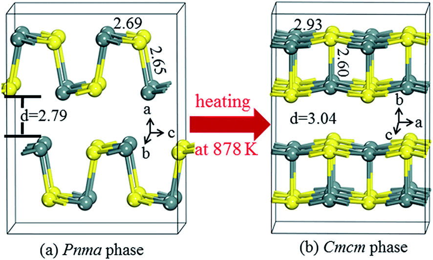 | ||
| Fig. 2 Crystal structures of SnS in (a) the Pnma phase and (b) the Cmcm phase. The unit of interatomic distance is in Å. Colour designations: Sn (grey) and S (yellow). | ||
3.2 Electronic band structures
The TE properties of crystalline materials are determined by their band structures. Therefore, we calculated the band structures of SnS within the Pnma and Cmcm phases; these results are shown in Fig. 3. In this figure, G, Z, T, Y, S, X, U, R describe the (0 0 0), (0 0 1/2), (−1/2 0 1/2), (−1/2 0 0), (−1/2 1/2 0), (0 1/2 0), (0 1/2 1/2), (−1/2 1/2 1/2) high-symmetry points, respectively. For both the Pnma and Cmcm phases, the conduction band minimum (CBM) is located at point G, and the valence band maximum (VBM) lies along the G–Z line, which results in an indirect band gap. The band gap is approximately 1.09 eV for the Pnma phase and 0.42 eV for the Cmcm phase; these values agree with the previously reported theoretical and experimental results,12,30,42–44 which vary in the range of 1.07–1.11 eV in the Pnma phase and are equal to 0.3 ± 0.1 eV in the Cmcm phase. The significantly smaller band gap in the Cmcm phase suggests that the bipolar conduction process occurs at high temperatures. | ||
| Fig. 3 Band structures of SnS in the Pnma (a) and Cmcm (b) phases. The energy zero is set to the valence-band maximum. The highest valence band and the lowest conduction band are highlighted in red. | ||
Because the transport properties are closely related to the electronic states near the highest valence band (HVB) and the lowest conduction band (LCB) for p- and n-type compounds, respectively, it is reasonable to focus on the energy range near the band gap. The valence and conduction bands are shown to have different characters: the heavy bands near the HVB contribute a high thermopower but exhibit a smaller carrier mobility, whereas the light bands near the LCB are expected to have a higher conductivity. We therefore anticipate different TE behaviours for p- and n-type doped materials. Further analysis of Fig. 3a and b shows that the bandwidths of both the HVB and LCB become larger when changing from the Pnma phase (0.65 eV for the HVB and 1.05 eV for the LCB, respectively) to the Cmcm phase (0.87 and 1.41 eV, respectively). Therefore, it is suggested that at the Pnma–Cmcm phase transition, there may be an enhancement of the conductivity.
Considering the calculated densities of state (DOS) in Fig. 4, we note that the 3s states of S are deep and separated from the other valence band states by a gap of approximately 4 eV, which indicates a strong lone electron pair character. The valence bands are formed primarily of the 5s and 5p states of Sn and the 3p states of S, whereas the conduction bands are primarily from the 5p and 3p states of Sn and S, respectively. Additionally, the valence band states from −4.7 to −1.4 eV are responsible for the strong Sn–S covalent bonds that are parallel to the slab layers, whereas those states from −1.4 to 0 eV contribute to the strong covalent bonds that are perpendicular to the slab layers.30
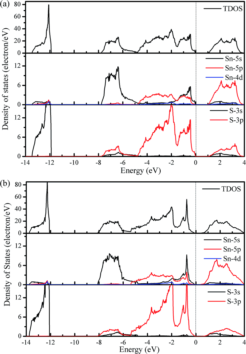 | ||
| Fig. 4 Total and partial densities of state for SnS within the Pnma (a) and Cmcm (b) structures. The energy zero is set to the VBM. | ||
Generally, materials with large Seebeck coefficients are usually associated with a large DOS near the band gap.45 The DOS plotted in Fig. 4 shows that the change in the height of the total DOS is not significant when going from the Pnma phase to the Cmcm phase; no apparent difference can be observed in the Seebeck coefficient between the Pnma and Cmcm phases. However, the HVB shows a higher DOS peak than the LCB, which is indicative of a higher Seebeck coefficient for p-type doping.
3.3 Thermoelectric properties
The transport properties calculated as a function of the carrier concentration from 300 to 1080 K are shown in Fig. 5. The calculated Seebeck coefficient (S) [Fig. 5(a1 and a2)] for both p- and n-type doped crystals are shown to be sensitive to the carrier concentration. S shows a near-linear increase as the carrier concentration decreases in the 300–800 K temperature range. As mentioned above, the calculated band gap for the Cmcm phase is 0.42 eV and thus likely leads to the bipolar effect (i.e., a decrease in the Seebeck coefficient with decreasing carrier concentration, which is the opposite of the usual situation). At 900–1080 K, bipolar conduction appears in the regime below carrier concentrations of 1.12 × 1019 cm−3; however, they are in a doping range that is significantly lighter than the likely optimal doping ranges, which are given as 4.63–8.01 × 1019 cm−3 for p-type and 12.21–14.02 × 1019 cm−3 for n-type at 900–1080 K (see Table 1). Therefore, the ZT value at high temperatures with low doping may be degraded by the bipolar effect; however, this will likely not occur at doping levels above 1.12 × 1019 cm−3. This finding is verified by the following results from Fig. 8b. In addition, the Seebeck coefficient strongly depends on the temperature, which is discussed below. | ||
| Fig. 5 Transport properties of SnS as a function of the carrier concentration in the temperature range of 300–1080 K: (a1) p-type Seebeck coefficients, S; (a2) n-type Seebeck coefficients, S; (b1) p-type electrical conductivities, σ; (b2) n-type electrical conductivities, σ; (c1) p-type power factors, S2σ; (c2) n-type power factors, S2σ. | ||
| T | p-type | κc | n-type | ||||||||
|---|---|---|---|---|---|---|---|---|---|---|---|
| Pa | MPFb | ZT | S | σ | na | MPFb | ZT | S | σ | ||
| a p and n are the optimal carrier concentrations for the p- and n-type materials, respectively. The units for T, p and n, MPF, S, and σ are K, 1019 cm−3, 10−4 W m−1 K−2, μV K−1 and 104 Ω−1 m−1, respectively.b MPF is the abbreviation of maximum power factor.c κ is the thermal conductivity of p- and n-type doping and the unit is in W m−1 K−1. | |||||||||||
| 300 | 2.75 | 2.05 | 0.04 | 131.20 | 1.19 | 1.40 | 6.68 | 1.26 | 0.03 | 65.29 | 2.95 |
| 400 | 3.48 | 2.98 | 0.11 | 143.90 | 1.44 | 1.12 | 7.05 | 1.92 | 0.07 | 79.38 | 3.05 |
| 500 | 4.66 | 3.96 | 0.21 | 146.17 | 1.85 | 0.94 | 7.50 | 2.64 | 0.14 | 91.15 | 3.17 |
| 600 | 5.55 | 4.96 | 0.37 | 152.43 | 2.14 | 0.81 | 7.59 | 3.38 | 0.25 | 103.85 | 3.14 |
| 700 | 7.02 | 5.96 | 0.58 | 152.78 | 2.57 | 0.72 | 8.19 | 4.16 | 0.40 | 112.66 | 3.28 |
| 800 | 7.79 | 6.93 | 0.85 | 159.64 | 2.72 | 0.65 | 9.33 | 4.97 | 0.61 | 117.74 | 3.58 |
| 900 | 4.63 | 7.49 | 1.04 | 131.27 | 4.35 | 0.65 | 12.21 | 7.41 | 1.03 | 111.51 | 5.96 |
| 1000 | 6.36 | 8.69 | 1.34 | 128.86 | 5.23 | 0.65 | 13.39 | 8.59 | 1.32 | 116.53 | 6.32 |
| 1080 | 8.01 | 9.69 | 1.63 | 127.94 | 5.92 | 0.65 | 14.02 | 9.52 | 1.59 | 121.40 | 6.46 |
The electrical conductivity (σ) is also important and is related to the relaxation time (τ). In this paper, the τ value (7.44 × 10⁻¹⁶ s) from the experimental measurements by Nassary et al.18 has been applied to the n-doped system. For the p-doped system, τ can be deduced using the 300 K data from Hegde et al.13 The reported experimental electrical resistivity ρ is 1.20 Ω m at this temperature, and the corresponding carrier concentration is 1.52 × 1015 cm−3, which can be combined with the calculated σ/τ to yield τ = 15.1 × 10⁻¹⁶ s. The obtained τ is near that used in the Ag-doped SnS systems (τ = 30 × 10−16 s).20 We then calculated σ by σ/τ × τ. The resulting p-type and n-type electrical conductivities are shown in Fig. 5(b1 and b2), respectively. It is shown that σ for both doping types substantially increases with increasing carrier concentration. For example, as the carrier concentration increases from 1018 to 1021 cm−3, σ at 900 K increases rapidly from 2.05 × 10³ to 2.29 × 10⁵ Ω−1 m−1 for p-type doping and from 9.67 × 10² to 2.48 × 10⁵ Ω−1 m−1 for n-type doping. However, the temperature dependence of the electrical conductivity is shown to be relatively weaker. As shown in Fig. 5(b1 and b2), the electrical conductivity gradually declines with temperature in the low-temperature Pnma phase. In the high-temperature Cmcm phase, σ shows an increasing trend at low doping but decreases at higher doping levels. The high-temperature conductivity is significantly higher with p-type doping but is not significantly higher for n-type doping. This can be explained by the band structure: the HVB becomes more dispersed in the Pnma phase compared to the Cmcm phase (see Fig. 3), which indicates a decreased effective mass of hole carrier and, thus, an increased electrical conductivity for p-type doping; however, the LCB changes little in going from the Pnma phase to the Cmcm phase (see Fig. 3). It indicates that there are no apparent changes in the effective mass of electron carrier and thus in the electrical conductivity for n-type doping from the Pnma phase to the Cmcm phase. σ is also significantly larger than those previously reported for pure SnS (e.g., below 500 Ω−1 m−1);19 the S is marginally lower than those of pure SnS (e.g., 350–750 μV K−1). The substantial increase in σ and the slight decrease in S could result in a net increase in S2σ (i.e., the power factor or PF), which is the numerator in the fractional expression of ZT. For example, for pure SnS at 823 K, the maximum power factor is 1.34 × 10⁻⁴ W m−1 K−2; for p-doped SnS at 800 K, an improved value of 6.93 × 10⁻⁴ W m−1 K−2 is obtained (Table 1).
In TE applications, PF (S2σ) is an important factor that directly influences TE performance. The PF for p- and n-type materials as a function of the carrier concentration is given in Fig. 5(c1 and c2), respectively. There is an optimal carrier concentration that yields the maximum PF (MPF). To obtain more detailed information, the optimal carrier concentration, MPF, ZT, S, and σ in the 300–1080 K temperature range are summarized in Table 1. These data indicate that as T increases, the MPF for both p- and n-type materials increases, and the optimal carrier concentration for n-type doping shifts to a higher level. For p-type doping, an increasing trend is shown at temperatures below 800 K; however, the optimal carrier concentration suddenly decreases at 900 K and then increases again as the temperatures increase above 900 K. At a given temperature, the n-type material has a higher optimal carrier concentration than the p-type but has lower MPF values; this result indicates that p-type SnS performs better in terms of TE properties than n-type SnS. For p-type SnS, the optimal carrier concentration varies from 2.75 to 8.01 × 1019 cm−3 and thus produces MPF values from 2.05 to 9.69 × 10⁻⁴ W m−1 K−2. Concurrently, n-doped counterparts exhibit MPF values from 1.26 to 9.52 × 10⁻⁴ W m−1 K−2 with carrier concentrations of 6.68–14.02 × 1019 cm−3. Consequently, we predict that SnS will exhibit better TE performance at high temperatures and with heavy doping.
The thermal conductivity of SnS was investigated from 300 to 800 K by Tan et al.19 They noted that the variations of κ with the doping concentration are weak; thus, it is reasonable to assume that κ is only related to the temperature in this study. The κ values in 300–800 K temperature range are obtained by fitting the experimental data from Tan et al.,19 as shown in Fig. 6. The thermal conductivity is shown to decrease rapidly from 1.40 to 0.65 W m−1 K−1 as T increases from 300 to 800 K. Of note, in the Cmcm phase, we set κ as a constant to the fitted value at 800 K (0.65 W m−1 K−1) based on the following facts. For SnSe,3 κ gradually decreases as the temperatures rise in the Pnma phase but changes little in the Cmcm phase; the values of κ are also similar near the phase-transition temperature (807 K). For example, the values of κ in W m−1 K−1 along the c axis are 0.24, 0.23, 0.22, 0.24 and 0.23 for 675 K, 725 K, 775 K, 825 K, and 875 K, respectively. The biggest difference between these values is smaller than 0.02 W m−1 K−1. SnS shows a similar structure to that of SnSe; therefore, they may have a similar trend in κ. Recently, Tan et al.23 showed that κ in W m−1 K−1 for a SnS-0.5% Ag sample were 0.49, 0.48, 0.44, and 0.46 for 775 K, 825 K, 875 K, and 925 K, respectively, which also indicated that the κ values for SnS are comparable in the neighbouring regimes of the phase transition (phase-transition temperature of SnS is 878 K). Therefore, reasonable ZT values for SnS in the Cmcm phase could be achieved using the fitted κ value at 800 K (0.65 W m−1 K−1).
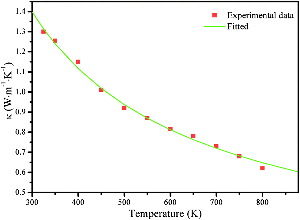 | ||
| Fig. 6 Thermal conductivity of SnS from ref. 19 and the fitted curve with the experimental data used in the proposed model, as discussed above. | ||
Combining the thermal conductivity with the electrical transport coefficients, we finally obtained the dimensionless figure of merit (ZT) as a function of the carrier concentration (see Fig. 7). In Fig. 7, it is shown that the ZT value can be significantly influenced by both the temperature and the carrier concentration. For both p- and n-type doping, the ZT value first increases with the carrier concentration, reaches an optimal value, and then decreases; these trends are similar to those found for the power factor. When the temperature rises from 300 to 800 K, the optimal ZT value increases from 0.04 to 0.85 for the p-type material and from 0.03 to 0.61 for the n-type material. With an additional increase in T, the optimal ZT continues to increase and is shown to be sensitive to temperature; it exceeds unity at 900 K and remains above it, reaching 1.63 for the p-type material and 1.59 for the n-type material at 1080 K. The strong temperature sensitivity shown makes a TE generator have a longer service life and a higher conversion efficiency in the high-temperature region. Such ZT–T behaviour in the high-temperature Cmcm phase is due to the strong temperature dependence of the Seebeck coefficient (see Fig. 8a). However, a high ZT peak value does not always indicate a high efficiency; the average ZT value over the imposed working temperature gradient is the critical factor. However, the high-temperature Cmcm phase does possess a high average ZT value of approximately 1.3 compared with the low-temperature Pnma phase (e.g., 0.3 ± 0.05). All of these findings indicate that the high-temperature Cmcm phase exhibits good TE performance; thus, this phase should be investigated in more detail. The higher ZT at high temperatures is primarily due to the higher electrical conductivity that is present at these temperatures. From Table 1, we also note that at high temperatures, the optimal carrier concentration for the p-type material is 4.63–8.01 × 1019 cm−3, which is substantially lower than that for the n-type material (e.g., 12.21–14.02 × 1019 cm−3). Such a doping concentration is most likely experimentally controllable for the p-type material but is relatively more difficult for the n-type material.
 | ||
| Fig. 7 Calculated ZT values as a function of the carrier concentration in the temperature range of 300–1080 K. | ||
 | ||
| Fig. 8 Temperature dependence of the Seebeck coefficient (a) and the ZT value (b) at various p-type doping levels. | ||
The data presented in this study are now compared with those obtained in previous studies. As stated above, a high ZT of 1.61 ± 0.02 for doped-SnS is achieved at 1080 K, which is approximately 10 times as much as the experimental intrinsic value (e.g., 0.16) of pure SnS.19 This finding indicates that doping and temperature play an important role in improving the ZT value of SnS. In particular, at 800 K, the optimal ZT value is predicted to be 0.85 (see Table 1) for the p-type material in this study, which agrees with that of the previously reported p-type SnS (ZT = 0.7).24 Recently, Tan et al.23 reported that a sample of SnS-0.5% Ag has a large ZT (0.6 at 923 K), which is smaller than that predicted at high temperatures. The large difference between these values is partially caused by the fact that the carrier concentration of the 0.5% Ag-doped SnS material does not reach the optimum doping level. For example, from 300 to 700 K, the carrier concentration of SnS-0.5% Ag ranges from 2.72–3 × 1018 cm−3, which is smaller by at least an order of magnitude than the predicted optimum doping level (e.g., 2.75–7.02 × 1019 cm−3) shown in this study. Those authors also showed that for Ag-doped SnS (see Fig. 3 in ref. 23), the ZT value at a given temperature first increases, then reaches a maximum value at x = 0.5 (x is the Ag content), and finally decreases above x = 0.5 in the Pnma phase as Ag doping increases from x = 0 to x = 2. This result indicates that there is an optimum doping level to achieve a peak ZT value. The electrical conductivity is shown to increase significantly due to Ag doping, which was also observed by Bera et al.20 These observed trends in ZT and σ are consistent with the results of this study. Unfortunately, experiments do not provide the corresponding carrier concentrations for different Ag doping levels at different temperatures; thus, we cannot make a further detailed comparison of these results with those reported in the literatures. In addition, in the context of this study, we observed that the ZT value for the high-temperature phase increases faster with temperature, which is in good agreement with the published measurements.
As expected, high ZT values can be achieved by cooperative tuning of the doping concentration and temperature. To better understand this synergetic effect, Fig. 8 shows the temperature dependence of the Seebeck coefficient and the ZT value for p-doped SnS at five different carrier concentrations (e.g., 4 × 10¹⁷, 2 × 10¹⁸, 2 × 10¹⁹, 1 × 10²⁰, and 1 × 1021 cm−3). Based on the results reported by Haas and his co-workers,14,44 the carrier concentration is equal to 4–5 × 1017 cm−3 for an undoped SnS crystal; therefore, we chose 4 × 1017 cm−3 to represent the intrinsic behaviour of SnS and thus selected 2 × 10¹⁸, 2 × 10¹⁹, 1 × 10²⁰, and 1 × 1021 cm−3 as four typical doping concentrations to compare with the intrinsic case. At low T (e.g., 300–800 K), there is no bipolar effect due to the large band gap; thus, the Seebeck coefficient in Fig. 8a shows an increasing trend in this temperature region, which is typical for a semiconductor. As the temperature increases further (e.g., 900–1080 K), minority carriers arise due to thermal excitation and the coexistence of majority and minority carriers leads to the so-called bipolar effect, which results in a decreasing trend in S at high T and below p = 1.12 × 1019 cm−3. For example, at p = 2 × 1018 cm−3, the Seebeck coefficient drops from 193.13 to 88.59 μV K−1 when the temperature changes from 900 to 1080 K. At p = 1.12 × 1019 cm−3 and above, the Seebeck coefficient does not enter the bipolar regime and thus exhibits the same trend as the low-temperature phase, which is favourable for the improvement of the ZT value in this carrier concentration regime. In Fig. 8b, at p = 4 × 1017 cm−3, the ZT value first increases with increasing T, and when T exceeds 800 K, ZT begins to drop due to bipolar conduction. In particular, the ZT value is low (e.g., less than 0.1); this indicates that undoped SnS is not a good TE material, even at high temperatures. At p = 2 × 1018 cm−3, there are no apparent changes in the ZT value compared to pure SnS. At p = 2 × 1019 cm−3 and above, the ZT value shows an overall increase as temperature increase. When T exceeds 800 K, the ZT value increases even faster with temperature; for example, the ZT value at p = 1 × 1020 cm−3 increases significantly from 0.84 for 800 K to 1.62 for 1080 K. This finding strongly suggests that the high-temperature Cmcm phase does not exhibit a better ZT value at low doping but does at higher doping. However, this does not mean that higher doping produces a better ZT value; for example, at p = 1 × 1021 cm−3, the observed ZT values are lower than those at p = 1 × 1020 cm−3. All of the abovementioned results undoubtedly show that the synergetic effect of the carrier concentration and temperature is important to obtain high ZT values in SnS crystals.
4. Conclusions
In summary, we have investigated the structural, electronic, and p- and n-type doped TE properties of SnS across the Pnma–Cmcm phase transition. An indirect bandgap is found at 1.09 eV and 0.42 eV for the Pnma and the Cmcm phases, respectively, and the significantly smaller bandgap in the Cmcm phase leads to the bipolar effect. In particular, the results of this study show that pure SnS does not exhibit good TE performance, even in the high-temperature Cmcm phase; this is significantly different from the case of pure SnSe, in which a higher ZT was found in the high-temperature phase. However, we can also obtain a superior ZT value in SnS crystal through the cooperative tuning of the carrier concentration and temperature. The optimum doping concentration is predicted to be (2.75–8.01) × 1019 cm−3 (p-type) and (6.68–14.02) × 1019 cm−3 (n-type) in the temperature range of 300–1080 K, which should be accessible for p-type but relatively more difficult for n-type. Under the optimal doping concentration, the peak ZT for the high-temperature phase remains above unity and reaches 1.63 (p-type) and 1.59 (n-type) at 1080 K, which is approximately 10 times larger than the maximum measured value of pure SnS. Conversely, the low-temperature phase exhibits a ZT of less than 1. Additionally, the average ZT at low temperatures (e.g., 0.31 ± 0.05) is much lower than that at high temperatures (e.g., approximately 1.3). These facts indicate that SnS might be modified to be a potential high-temperature TE material. Additionally, these findings tell us that the high-temperature Cmcm phase of SnS should be studied in more detail. The high ZT in doped SnS can be attributed to its enhanced electrical conductivity. The calculated results reported in this study should be helpful in understanding the TE behaviour of other IV–VI group compound systems.Acknowledgements
This work was supported by the China Postdoctoral Science Foundation (2014M551848), the NSFC project (no. 91122015 and 21303025), Guangxi Natural Science Foundation of China (2014GXNSFBA118029), and the Foundation of the Key Laboratory of Coal to Ethylene Glycol and Its Related Technology of Chinese Academy of Sciences (201401).Notes and references
- G. J. Snyder and E. S. Toberer, Nat. Mater., 2008, 7, 105 CrossRef CAS PubMed.
- K. Biswas, J. He, I. D. Blum, C. I. Wu, T. P. Hogan, D. N. Seidman, V. P. Dravid and M. G. Kanatzidis, Nature, 2012, 489, 414 CrossRef CAS PubMed.
- L. D. Zhao, S. H. Lo, Y. Zhang, H. Sun, G. Tan, C. Uher, C. Wolverton, V. P. Dravid and M. G. Kanatzidis, Nature, 2014, 508, 373 CrossRef CAS PubMed.
- S. Sassi, C. Candolfi, J. B. Vaney, V. Ohorodniichuk, P. Masschelein, A. Dauscher and B. Lenoir, Appl. Phys. Lett., 2014, 104, 212105 CrossRef PubMed.
- C. L. Chen, H. Wang, Y. Y. Chen, T. Day and J. Snyder, J. Mater. Chem. A, 2014, 2, 11171 CAS.
- J. Carrete, N. Mingo and S. Curtarolo, Appl. Phys. Lett., 2014, 105, 101907 CrossRef PubMed.
- D. P. Spitzer, J. Phys. Chem. Solids, 1970, 31, 19 CrossRef CAS.
- H. J. Goldsmid, Proc. Phys. Soc. B, 1956, 69, 203 CrossRef.
- K. Takahata, Y. Iguchi, D. Tanaka, T. Itoh and I. Terasaki, Phys. Rev. B: Condens. Matter Mater. Phys., 2000, 61, 12551 CrossRef CAS.
- T. Caillat, A. Borshchevsky and J. P. Fleurial, J. Appl. Phys., 1996, 80, 4442 CrossRef CAS PubMed.
- Y. Kawaharada, K. Kurosaki, M. Uno and S. Yamanaka, J. Alloys Compd., 2001, 315, 193 CrossRef CAS.
- J. Vidal, S. Lany, M. d'Avezac, A. Zunger, A. Zakutayev, J. Francis and J. Tate, Appl. Phys. Lett., 2012, 100, 032104 CrossRef PubMed.
- S. S. Hegde, A. G. Kunjomana, K. A. Chandrasekharan, K. Ramesh and M. Prashantha, Phys. B, 2011, 406, 1143 CrossRef CAS PubMed.
- C. Haas and M. M. G. Corbey, J. Phys. Chem. Solids, 1961, 20, 197 CrossRef CAS.
- Y. Jayasree, U. Chalapathi, P. Uday Bhaskar and V. S. Raja, Appl. Surf. Sci., 2012, 258, 2732 CrossRef CAS PubMed.
- T. H. Patel, R. Vaidya and S. G. Patel, High Pressure Res., 2003, 23, 417 CrossRef CAS PubMed.
- B. Nariya, A. Dasadia, M. Bhayani, A. Patel and A. Jani, Chalcogenide Lett., 2009, 6, 549 CAS.
- M. M. Nassary, J. Alloys Compd., 2005, 398, 21 CrossRef CAS PubMed.
- Q. Tan and J. F. Li, J. Electron. Mater., 2014, 43, 2435 CrossRef CAS PubMed.
- C. Bera, S. Jacob, I. Opahle, N. S. H. Gunda, R. Chmielowski, G. Dennler and G. K. H. Madsen, Phys. Chem. Chem. Phys., 2014, 16, 19894 RSC.
- T. Chattopadhyay, A. Werner, H. G. von Schnering and J. Pannetier, Rev. Phys. Appl., 1984, 19, 807 CrossRef CAS.
- T. Chattopadhyay, J. Pannetier and H. G. Von Schnering, J. Phys. Chem. Solids, 1986, 47, 879 CrossRef CAS.
- Q. Tan, L. D. Zhao, J. F. Li, C. F. Wu, T. R. Wei, Z. B. Xing and M. G. Kanatzidis, J. Mater. Chem. A, 2014, 2, 17302 CAS.
- D. Parker and D. J. Singh, J. Appl. Phys., 2010, 108, 083712 CrossRef PubMed.
- D. I. Bletskan, J. Ovonic Res., 2005, 1, 47 Search PubMed.
- G. Kresse and J. Furthmüller, Phys. Rev. B: Condens. Matter Mater. Phys., 1996, 54, 11169 CrossRef CAS.
- P. E. Blöchl, Phys. Rev. B: Condens. Matter Mater. Phys., 1994, 50, 17953 CrossRef.
- J. P. Perdew, K. Burke and M. Ernzerhof, Phys. Rev. Lett., 1996, 77, 3865 CrossRef CAS.
- J. Heyd, G. E. Scuseria and M. Ernzerhof, J. Chem. Phys., 2003, 118, 8207 CrossRef CAS PubMed.
- A. Ettema, R. de Groot, C. Haas and T. Turner, Phys. Rev. B: Condens. Matter Mater. Phys., 1992, 46, 7363 CrossRef CAS.
- J. M. Chamberlain and M. Merdan, J. Phys. C: Solid State Phys., 1977, 10, L571 CrossRef CAS.
- A. D. Becke and E. R. Johnson, J. Chem. Phys., 2006, 124, 221101 CrossRef PubMed.
- M. César, Y. Ke, W. Ji, H. Guo and Z. Mi, Appl. Phys. Lett., 2011, 98, 2107 CrossRef PubMed.
- G. K. H. Madsen and D. J. Singh, Comput. Phys. Commun., 2006, 175, 67 CrossRef CAS PubMed.
- M.-S. Lee and S. D. Mahanti, Phys. Rev. B: Condens. Matter Mater. Phys., 2012, 85, 165149 CrossRef.
- S. Ahmad and S. D. Mahanti, Phys. Rev. B: Condens. Matter Mater. Phys., 2010, 81, 165203 CrossRef.
- B.-L. Huang and M. Kaviany, Phys. Rev. B: Condens. Matter Mater. Phys., 2008, 77, 125209 CrossRef.
- C. Wang, Y. Wang, G. Zhang and C. Peng, J. Phys. Chem. C, 2013, 117, 21037 CAS.
- P. Lu, C. Wu, Y. Li, Z. Yu, H. Cao, T. Gao and S. Wang, J. Mater. Sci., 2013, 48, 4999 CrossRef CAS.
- V. K. Gudelli, V. Kanchana, S. Appalakondaiah, G. Vaitheeswaran and M. C. Valsakumar, J. Phys. Chem. C, 2013, 117, 21120 CAS.
- Y. Wang, X. Chen, T. Cui, Y. Niu, Y. Wang, M. Wang, Y. Ma and G. Zou, Phys. Rev. B: Condens. Matter Mater. Phys., 2007, 76, 155127 CrossRef.
- L. A. Burton, D. Colombara, R. D. Abellon, F. C. Grozema, L. M. Peter, T. J. Savenije, G. Dennler and A. Walsh, Chem. Mater., 2013, 25, 4908 CrossRef CAS.
- F. Ke, J. Yang, C. Liu, Q. Wang, Y. Li, J. Zhang, L. Wu, X. Zhang, Y. Han, B. Wu, Y. Ma and C. Gao, J. Phys. Chem. C, 2013, 117, 6033 CAS.
- W. Albers, C. Haas and F. van der Maesen, J. Phys. Chem. Solids, 1960, 15, 306 CrossRef CAS.
- X. Gao, K. Uehara, D. D. Klug, S. Patchkovskii, J. S. Tse and T. M. Tritt, Phys. Rev. B: Condens. Matter Mater. Phys., 2005, 72, 125202 CrossRef.
Footnote |
| † Electronic supplementary information (ESI) available. See DOI: 10.1039/c5ra06134b |
| This journal is © The Royal Society of Chemistry 2015 |