DOI:
10.1039/C5RA05991G
(Paper)
RSC Adv., 2015,
5, 60804-60813
Artificial inverted compound eye structured polymer films with light-harvesting and self-cleaning functions for encapsulated III–V solar cell applications†
Received
3rd April 2015
, Accepted 9th July 2015
First published on 9th July 2015
Abstract
We report the artificial inverted compound eye structured (ICESs) polydimethylsiloxane (PDMS) films with light-harvesting and self-cleaning functions for the enhancement of solar power generation in encapsulated III–V gallium arsenide (GaAs) single-junction solar cells. The ICESs PDMS films are fabricated by facile, simple, and cost-effective soft lithography using sapphire master molds with the CESs consisting of hierarchical nanotextures/periodic microgratings prepared by thermally dewetted gold nanopatterning and subsequent dry etching processes. By attaching the ICESs PDMS film with a hydrophobic surface (i.e., water contact angle (θCA) of ∼121°) to the coverglass, the total and diffuse transmittances of the coverglass are simultaneously increased over a wide wavelength range of 350–900 nm, exhibiting higher solar weighted transmittance (SWT) of ∼94.3% and average haze ratio (Havg) of ∼67.6% than those of the bare coverglass (i.e., θCA ≈ 32°, SWT ≈ 90.2%, and Havg ≈ 4.1%, respectively). The resulting encapsulated III–V GaAs single-junction solar cells with the ICESs PDMS/coverglass show an enhanced power conversion efficiency (PCE) of 24.3% compared to the encapsulated solar cell with the bare coverglass (i.e., PCE = 22.96%) due to the increased short circuit current density from 26 to 27.64 mA cm−2, indicating the PCE increment percentage of ∼5.8%. Moreover, it also exhibits superior device performance at varying angles of incident light. For the long-term self-cleaning effect on the device efficiency, there is no significant variation in the PCE after approximately one month, indicating a low PCE drop percentage of ∼1.4%.
Introduction
Recently, there has been growing interest for the enhancement of solar energy harvesting in solar cells owing to the energy crisis and environmental issues. To effectively harvest sunlight in solar cells, an efficient antireflection layer, which can suppress the surface Fresnel reflection losses at the interface between the air and top surface of solar cells over a broad solar spectral range, is vital.1–3 Actually, for practical applications of solar cells, the antireflection layer should be considered to reduce the reflection at the module level including coverglasses and encapsulants.2–7 However, the conventional dielectric material-based thin-film antireflection layers such as magnesium fluorides and porous silicon oxides, which have some drawbacks including durability issues, thermal expansion mismatch, poor or reduced adhesion on certain substrates, sensitivity to thickness variations, and material selection as well as narrow low reflection band for incident wavelengths and angles,8–10 may not be suitable under real harsh environments. As an alternative of conventional antireflection layers, over the past years, there have been many studies on the efficiency enhancement of solar cells with textured surfaces (i.e., biomimetic micro- or nanostructures) for efficient antireflection and light scattering.11–15 Particularly, artificial compound eye structures (CESs) inspired from corneas of insects, which are usually composed of thousands of microstructures covered with nanonipple arrays, effectively reduce the surface reflection (or enhance the transmission) over wide ranges of incident wavelengths and angles because of the formation of the effective gradient-refractive-index profile between air and the bulk surface.16–22 Besides, the CESs with microscale periods can also extend the effective optical paths and promote the transmitted diffuse lights, while keeping high total transmission properties (e.g., high optical haze).23–26 In addition, due to this extension of optical paths, the microstructures (e.g., microlenses, microcones) can help to reduce total internal reflection losses in optoelectronic devices like light-emitting diodes.27,28
On the other hand, polydimethylsiloxane (PDMS) is widely used as conformable and elastomeric replica stamps, substrates, or membranes in the soft lithography, which is relatively a more simple, large-scalable, and cost-effective micro- and nanopatterning technique with high-throughput production compared to the energy-intensive patterning methods such as electron-beam lithography, nanoimprint lithography, and photolithography, owing to its low free surface energy, flexibility, transparency, and hardness.29–33 Furthermore, the PDMS can be suitable as an antireflective protection layer of the coverglass in encapsulated solar cells because of its lower refractive index of ∼1.4–1.43 (i.e., n ≈ 1.5–1.52 for glass).32–35 Also, the cured PDMS film attached on other flat substrates such as wafers and glasses has shown a very good and strong adhesion property due to the mainly van der Waals force (e.g., adhesive strengths of ∼180 kPa).36,37 Therefore, the PDMS film can not only be powerfully well-laminated on the flat surface of coverglasses, but also reversibly easily-detached from it. From these reasons, as an antireflective protection layer of coverglasses, the compound eye structured PDMS film with high optical transparency and haze can boost the light harvesting in the underneath encapsulated solar cells, resulting in the efficiency improvement of devices. In addition, for photovoltaic industry applications, mass production would be also possible because the large-scale fabrication techniques of micro- and nanostructured polymer films have been developed by roll-to-roll or roll-to-plate processes using the soft imprint lithography.38–40 Meanwhile, the roughened structures could enhance the surface hydrophobicity of materials, related to the Cassie–Baxter wetting behavior.41,42 This hydrophobic surface, which can self-clean the dust particles and contaminants on the surface, is exceedingly useful in practical solar cell applications.35,43,44 Thus, it is very meaningful to analyze the optical properties and water wettability by applying the hierarchical nano/microstructures into the surface of PDMS films as the antireflective protection layer of coverglasses for efficiency improvement of encapsulated solar cells. In this work, we fabricated the artificial inverted CESs (ICESs) on the surface of PDMS films by the soft lithography method using sapphire master molds with the CESs prepared by thermally dewetted gold (Au) nanopatterning and dry etching processes. Their water wetting behaviors as well as optical properties were studied. The effect of the ICESs PDMS film as an antireflection layer of coverglasses on the device characteristics of encapsulated gallium arsenide (GaAs) single-junction solar cells was investigated. For a theoretical analysis of optical light scattering properties, the finite-difference time-domain (FDTD) simulation was performed. Besides, the incident light angle-dependent device performance and the long-term device stability for demonstrating the self-cleaning function were also explored.
Experimental and numerical modeling details
Fabrication of ICESs PDMS films
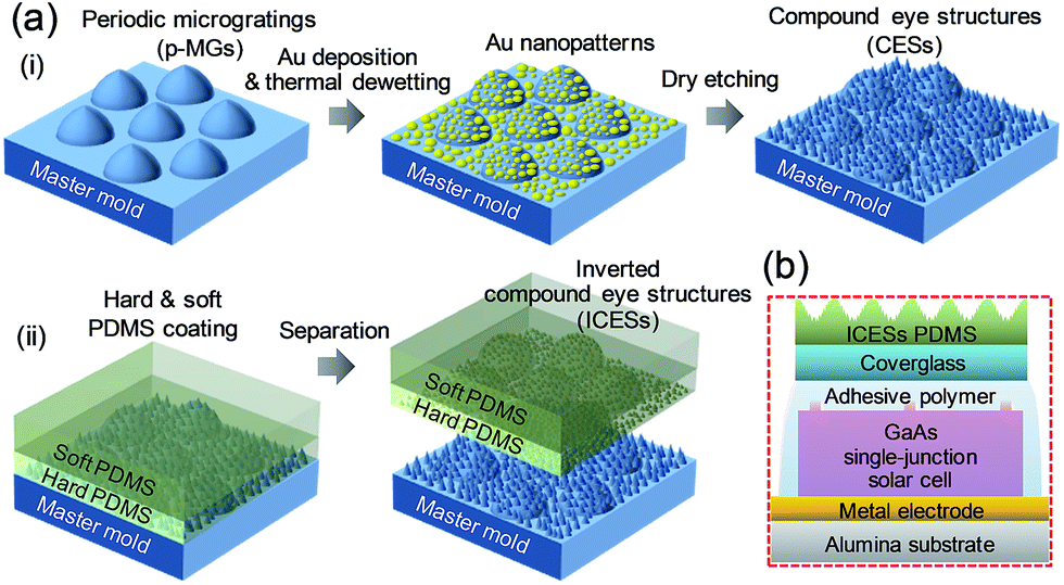
Fig. 1 shows schematic illustrations of (a) fabrication process steps for (i) CESs on the master mold by thermally dewetted Au nanopatterns and dry etching and (ii) ICESs on the PDMS film using the CESs patterned mold by the soft lithography method and (b) encapsulated III–V GaAs single-junction solar cell structure with the ICESs PDMS film/coverglass. For the master mold with CESs, the patterned sapphire substrates, which were purchased from AND Corporation, consisting of conical periodic microgratings (p-MGs) with two-dimensional hexagonal pattern arrays, having the average height and period of ∼1.5 ± 0.1 μm and ∼2.5 ± 0.1 μm, respectively, were used. For the formation of closely-packed nanotextures (NTs) with periods smaller than 200 nm, the Au thin film with a thickness of 4 nm was deposited on the p-MGs/sapphire substrate by a thermal evaporation system. And then, the samples were heat-treated by using a rapid thermal annealing system at a temperature of 600 °C for 2 min in a nitrogen environment. In this case, the Au thin film was agglomerated into the nanosized particles due to its increased surface energy by the heat (see Fig. S1 in the ESI†).16,45 Using the Au nanopatterns as an etch mask, the NTs on the surface of p-MGs/sapphire substrates were fabricated, thus creating the compound eye structures (CESs), as shown in Fig. 1(a)(i). The dry etching was performed with 50 W of RF power and 200 W of additional ICP power at 3 mTorr of process pressure for 7 min in Ar/Cl2/BCl3 (2![[thin space (1/6-em)]](https://www.rsc.org/images/entities/char_2009.gif) :1:4) plasma. The remaining Au was removed using the etchant solution based on potassium iodide and iodine (KI/I2). To fabricate the ICESs on the surface of PDMS films, as shown in Fig. 1(a)(ii), a hard PDMS, which was often used to prevent the deformation and distortion of replica nanofeatures,46 was prepared by mixing a 3.4 g of trimethylsiloxyterminated vinylmethylsiloxane-dimethylsiloxane (VDT-731; Gelest, Inc.), one drop of a platinum catalyst (platinum divinyltetramethyldisiloxane, SIP6831.2; Gelest, Inc.), and two drops of a modulator (1,3,5,7-tetravinyl-1,3,5,7-tetramethylcyclotetrasiloxane, SIT 7900.0; Gelest, Inc.). After that, the methylhydrosiloxane-dimethylsiloxane (HMS-301; Gelest, Inc.) was added into this mixture with subsequent stirring for 2 min and degassing for 5 min in the vacuum desiccators. Afterwards, the hard PDMS was spin-coated on the fabricated master molds with CESs at 1000 rpm for 40 s and 500 rpm for 5 min, sequentially, followed by curing at a temperature of 75 °C for 25 min in an oven. As a nondestructive and reversible manner, to enable manual application and intimate conformable contact on flat surfaces, after degassing the Sylgard 184 (Dow Corning Co.) polymer with a ratio of 10:1 (base:agent) for 1 h, which is the soft PDMS, it was poured on the hard PDMS/master molds, and then the samples were cured at 75 °C for 2 h in an oven. Finally, the PDMS films (hard/soft PDMS) were carefully separated from the master molds, which resulted in the inverted compound eye structured (ICESs) PDMS films with a size of 2 × 2 cm2 and a thickness of ∼300 μm. For comparison, the inverted NTs (INTs) PDMS film was also fabricated using the flat sapphire substrate with NTs by the same fabrication process. For the epitaxial growth of GaAs single-junction solar cell structure, an AIXTRON multi-wafer metal organic chemical vapor deposition reactor was used on 2° misoriented n-type GaAs substrate from (100) towards (111) direction. The GaAs single-junction solar cells with a chip aperture area of 0.3025 cm2 including metal contact grids were fabricated by conventional photolithography, metal evaporation, lift-off, and etch processes. And then, the cells were integrated on metal-coated alumina-based printed circuit boards by bonding the top Au wires and the rear silver paste. The cells on printed circuit boards were completely encapsulated with an ultraviolet curable adhesive (NOA 89, Norland Products Inc.) and a cost-effective soda lime float coverglasses (Microscope slides, Sail brand, Cat. no. 7101, manufactured by Yancheng Huida medical instruments Co., China) with a size of 1 × 1 cm2. The NOA89 adhesive was poured onto the cells bonded on printed circuit boards and subsequently covered by the coverglass, followed by exposing an ultraviolet source, which is a 40 W-mercury ultraviolet lamp with a light emission wavelength range of 297–435 nm, for 20 min to cure the NOA 89 adhesive. As can be seen in Fig. 1(b), to improve the light harvesting in the underneath cell absorption layer, the fabricated ICESs PDMS films with a size of 1 × 1 cm2 were laminated on the coverglass of encapsulated III–V GaAs single-junction solar cells as an antireflective protective layer.
:1:4) plasma. The remaining Au was removed using the etchant solution based on potassium iodide and iodine (KI/I2). To fabricate the ICESs on the surface of PDMS films, as shown in Fig. 1(a)(ii), a hard PDMS, which was often used to prevent the deformation and distortion of replica nanofeatures,46 was prepared by mixing a 3.4 g of trimethylsiloxyterminated vinylmethylsiloxane-dimethylsiloxane (VDT-731; Gelest, Inc.), one drop of a platinum catalyst (platinum divinyltetramethyldisiloxane, SIP6831.2; Gelest, Inc.), and two drops of a modulator (1,3,5,7-tetravinyl-1,3,5,7-tetramethylcyclotetrasiloxane, SIT 7900.0; Gelest, Inc.). After that, the methylhydrosiloxane-dimethylsiloxane (HMS-301; Gelest, Inc.) was added into this mixture with subsequent stirring for 2 min and degassing for 5 min in the vacuum desiccators. Afterwards, the hard PDMS was spin-coated on the fabricated master molds with CESs at 1000 rpm for 40 s and 500 rpm for 5 min, sequentially, followed by curing at a temperature of 75 °C for 25 min in an oven. As a nondestructive and reversible manner, to enable manual application and intimate conformable contact on flat surfaces, after degassing the Sylgard 184 (Dow Corning Co.) polymer with a ratio of 10:1 (base:agent) for 1 h, which is the soft PDMS, it was poured on the hard PDMS/master molds, and then the samples were cured at 75 °C for 2 h in an oven. Finally, the PDMS films (hard/soft PDMS) were carefully separated from the master molds, which resulted in the inverted compound eye structured (ICESs) PDMS films with a size of 2 × 2 cm2 and a thickness of ∼300 μm. For comparison, the inverted NTs (INTs) PDMS film was also fabricated using the flat sapphire substrate with NTs by the same fabrication process. For the epitaxial growth of GaAs single-junction solar cell structure, an AIXTRON multi-wafer metal organic chemical vapor deposition reactor was used on 2° misoriented n-type GaAs substrate from (100) towards (111) direction. The GaAs single-junction solar cells with a chip aperture area of 0.3025 cm2 including metal contact grids were fabricated by conventional photolithography, metal evaporation, lift-off, and etch processes. And then, the cells were integrated on metal-coated alumina-based printed circuit boards by bonding the top Au wires and the rear silver paste. The cells on printed circuit boards were completely encapsulated with an ultraviolet curable adhesive (NOA 89, Norland Products Inc.) and a cost-effective soda lime float coverglasses (Microscope slides, Sail brand, Cat. no. 7101, manufactured by Yancheng Huida medical instruments Co., China) with a size of 1 × 1 cm2. The NOA89 adhesive was poured onto the cells bonded on printed circuit boards and subsequently covered by the coverglass, followed by exposing an ultraviolet source, which is a 40 W-mercury ultraviolet lamp with a light emission wavelength range of 297–435 nm, for 20 min to cure the NOA 89 adhesive. As can be seen in Fig. 1(b), to improve the light harvesting in the underneath cell absorption layer, the fabricated ICESs PDMS films with a size of 1 × 1 cm2 were laminated on the coverglass of encapsulated III–V GaAs single-junction solar cells as an antireflective protective layer.
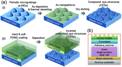 |
| | Fig. 1 Schematic illustrations of (a) fabrication process steps for (i) CESs on the master mold by thermally dewetted Au nanopatterns and dry etching and (ii) ICESs on the PDMS film using the CESs patterned mold by the soft lithography method and (b) encapsulated III–V GaAs single-junction solar cell structure with the ICESs PDMS film/coverglass. | |
Characterization instruments
Field-emission scanning electron microscope (FE-SEM; LEO SUPRA 55, Carl Zeiss) and atomic force microscope (AFM; D3100, Veeco) measurements were carried out to investigate surface morphologies and patterned profiles of the fabricated samples. The optical transmittance and reflectance properties were characterized by using a UV-vis-NIR spectrophotometer (Cary 5000, Varian) with an integrating sphere (see Fig. S2 in the ESI†). The water contact angles were measured and averaged at three different positions on the surface of samples by using a contact angle measurement system (Phoenix-300, SEO Co., Ltd) with ∼5 μL droplets of de-ionized water at room temperature. A solar simulator (WXS-220S-L2, Wacom) was used for current–voltage measurements of devices under 1-sun air mass 1.5 global illumination. The external quantum efficiency (EQE) was characterized by using a QEX7 system (PV Measurements, Inc.).
Numerical modelling and simulations
The theoretical calculation on an optical light scattering behavior of the ICES PDMS film was performed using the FDTD method. For the FDTD optical simulations, a commercial software (FullWAVE, Rsoft Design Group) was utilized.47 To design the theoretical model, in calculations, the hierarchical inverted nanotextures (nanocones)/periodic microgratings on the surface of PDMS film were represented by a periodic geometry in the Cartesian coordinate system by a scalar-valued function of two variables, f(x, z), for simplicity. It was assumed that the incident light entered from air into the structure at normal incidence. The amplitude of y-polarized electric field (Ey) was calculated for the incident plane wave with a slab mode beam profile in the continuous-wave mode, which was normalized at a wavelength (λ) = 532 nm. Here, perfectly-matched-layer boundary conditions were enforced. The simulation time step and time were set to be 3 nm per c and 300 μm per c, where c is the speed of light in vacuum, respectively, with a grid size of 5 nm. For the PDMS, the refractive index was assumed to be 1.43 while the extinction coefficient was not considered because it can be ignored.
Results and discussion
Surface morphologies and patterned profiles
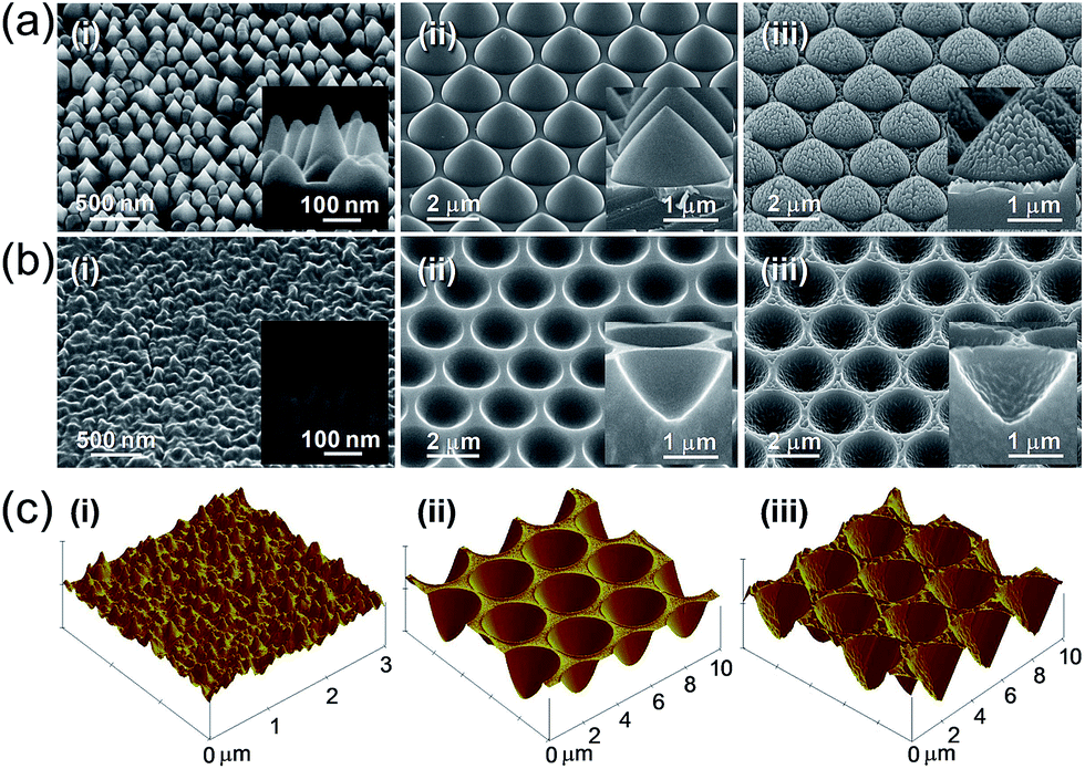
Fig. 2 shows the FE-SEM images of (a) sapphire master molds with (i) the flat NTs, (ii) the p-MGs, and (iii) the CESs and (b) PDMS films with inverted patterns of the corresponding master molds. For the PDMS films with (i) the flat INTs, (ii) the p-IMGs, and (iii) the ICESs in Fig. 2(b), AFM images are also shown in Fig. 2(c). As shown in Fig. 2(a), the NTs, p-MGs, and CESs (i.e., hierarchical NTs/p-MGs) were well formed on the surfaces of corresponding master molds, respectively. By using the soft lithography, the micrograting arrayed patterns on sapphire master molds were negatively well transferred into the surface of PDMS films without any deformation and distortion, as shown in Fig. 2(b)(ii) and (iii). However, the nanotextured patterns on the master mold with the average height of ∼180 ± 20 nm were poorly copied on the surface of PDMS film in spite of the use of hard PDMS. This may be attributed to the very closely-packed patterns of NTs (i.e., high density of ∼70%) with the low average period of ∼100 ± 20 nm, and thus the hard PDMS solution could not wedge into the empty space between the NTs. As a result, the INTs with a low average depth of ∼90 ± 10 nm were formed on the surfaces of flat and periodic inverted microgratings (p-IMGs) PDMS films, as can be seen in Fig. 2(b)(i) and (iii). Nevertheless, the relatively favorable INTs, p-IMGs, and ICESs patterns were formed on the surface of PDMS films from the corresponding master molds, respectively, by the soft lithography pattern transfer method, which can be also confirmed in the AFM images of Fig. 2(c).
 |
| | Fig. 2 FE-SEM images of (a) sapphire master molds with (i) flat NTs, (ii) p-MGs, and (iii) CESs and (b) PDMS films with inverted patterns of the corresponding master molds and (c) AFM images of the PDMS films with (i) flat INTs, (ii) p-IMGs, and (iii) ICESs. | |
Surface wettability and self-cleaning behaviors
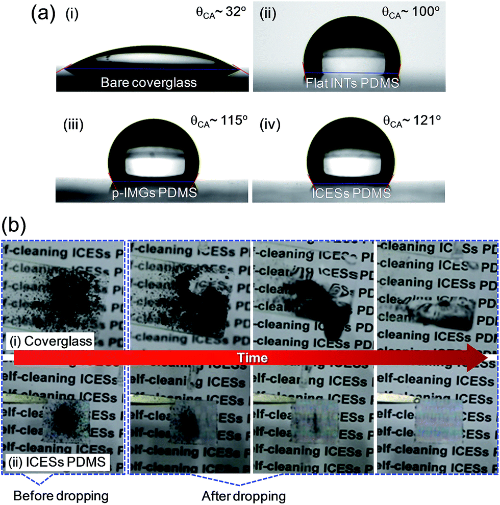
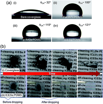
The dust particles on the surface of coverglass can be harmful to the performance of encapsulated solar cells under real outdoor environments.35,48 Therefore, it is necessary to employ the antireflection layer with a self-cleaning function. For the samples with different surface morphologies, the water contact angles were measured to investigate the wetting behavior. Fig. 3 shows the photographs of (a) a water droplet on (i) the bare coverglass and the PDMS films with (ii) flat INTs, (iii) p-IMGs, and (iv) ICESs and (b) water droplet cleaning behaviors of (i) the bare coverglass and (ii) the PDMS film with the ICESs. As shown in Fig. 3(a), the bare coverglass had a hydrophilic surface with a water contact angle (θCA) of ∼32° while the patterned PDMS films showed the θCA values of >90° (i.e., hydrophobicity). In particular, the surface of the ICESs PDMS film exhibited the θCA value of ∼121° which is higher than those of the other PDMS films (i.e., θCA ∼ 100° and 115° for the PDMS films with the flat INTs and the p-IMGs, respectively). This is ascribed to the increased roughness on the surface of PDMS films with the hydrophobicity, i.e., θCA ≈ 95° for the flat bare PDMS film (see Fig. S3 in the ESI†), which can be explained by the Cassie–Baxter theory.41,42 This θCA value of ∼121° is relatively lower than those (i.e., θCA > 150°, superhydrophobicity) reported in other previous works.35,42–44 However, as can be seen in Fig. 3(b), after dropping the water droplets, the black charcoal particles on the ICESs PDMS film were clearly removed by the rolling down water droplets (i.e., self-cleaning). On the other hand, the black charcoal (or dust) particles on the bare coverglass were just relocated, thus partially remaining with water droplets at the edge of coverglass (see Fig. S4 and Video in the ESI†). Thus, this ICESs PDMS film with a hydrophobic surface is very useful because an optical interface with an additional self-cleaning effect would enhance the practical feasibility in outdoor environments.
 |
| | Fig. 3 Photographs of (a) a water droplet on (i) bare coverglass and the PDMS films with (ii) flat INTs, (iii) p-IMGs, and (iv) ICESs and (b) water droplet cleaning behaviors of (i) bare coverglass and (ii) PDMS film with the ICESs. The θCA is a water contact angle. | |
Optical properties
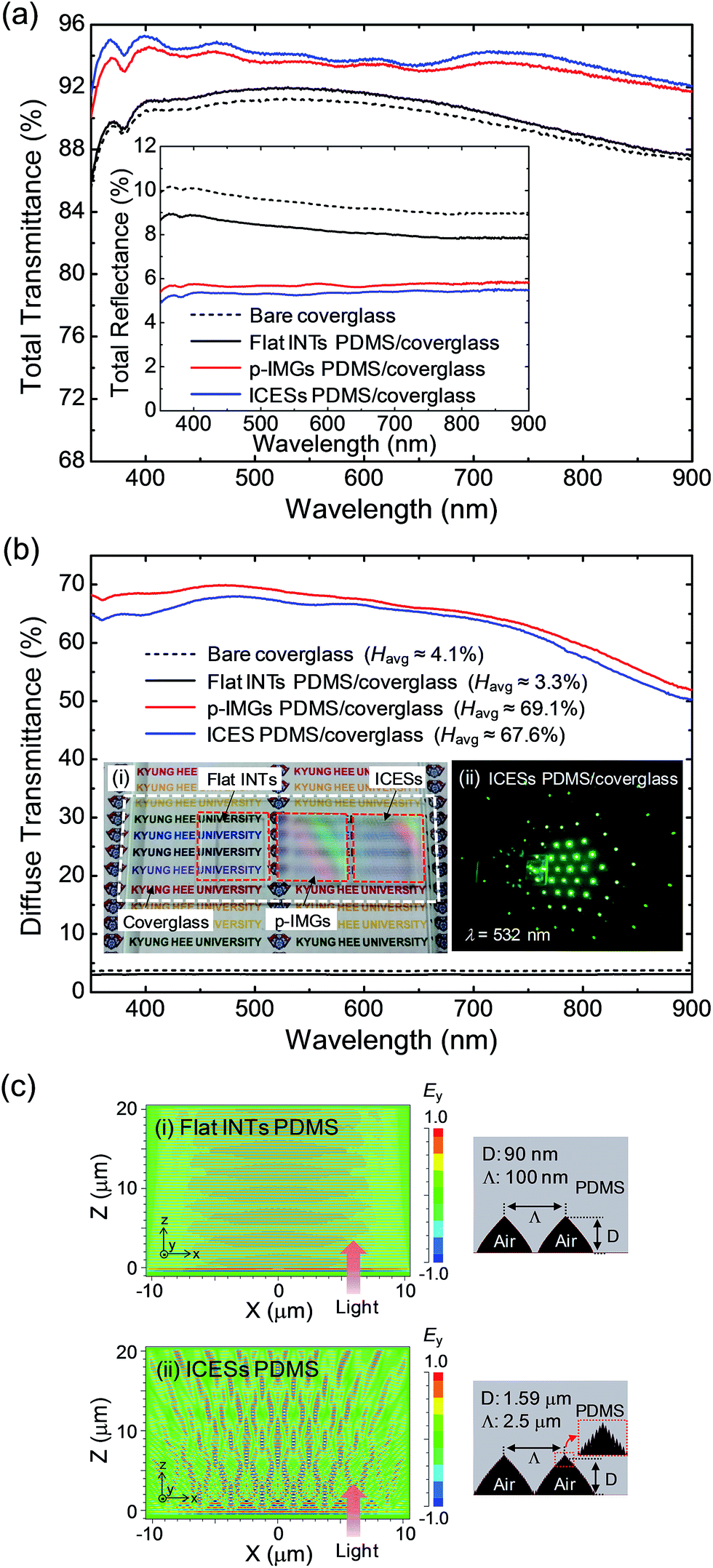
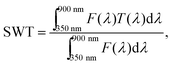
Fig. 4 shows the measured (a) total and (b) diffuse transmittance spectra of the PDMS films with the flat INTs, the p-IMGs, and the ICESs laminated on the coverglasses. For comparison, the total and diffuse transmittance spectra of the bare coverglass are also shown in Fig. 4(a) and (b), respectively. As shown in Fig. 4(a), by attaching the PDMS film with the flat INTs on the coverglass, the total transmittance was increased compared to the coverglass over a wide wavelength range of 350–900 nm due to the formation of a linear gradient-refractive-index profile between air and the PDMS caused by the INTs as well as the step gradient-refractive-index variation in the constituent materials from air (n = 1) to the coverglass (n ≈ 1.53) via the PDMS (n ≈ 1.4–1.43).49,50 For the p-IMGs PDMS film, on the contrary, the total transmittance spectrum was higher than that of the flat INTs PDMS film. This is the reason why the inverted conical microgratings with a grooved geometry feature have a more linear gradient-refractive-index profile from air to the PDMS due to the large depth of ∼1.5 μm and also lead to the extension of effective optical path lengths caused by the diffracted and rebounded lights between the inverted microgratings,24,51,52 which can effectively enhance the transmission in transparent materials by suppressing the surface reflection. By introducing the nanotextures on the p-IMGs (i.e., ICESs), the total transmittance was further increased, exhibiting the average total transmittance (Tavg) of ∼94.1% which is a higher value than those of the other samples (i.e., Tavg ≈ 90, 90.6, and 93.3% for the bare coverglass, the flat INTs PDMS/coverglass, and the p-IMGs PDMS/coverglass, respectively). This can be also explained by the increased trapping of the reflected lights from escaping back to air due to the INTs which have the small period of ∼100 nm and the effective homogeneous medium with a gradient-refractive-index profile. Therefore, the ICESs can further reduce the reflection or enhance the transmission.16–26 The light diffraction behaviors in these samples will be covered in the paragraph of Fig. 4(b). For solar cell applications, the solar weighted transmittance (SWT) was estimated using a well-known equation:53| |
 | (1) |
where F(λ) is a spectral photon irradiance (i.e., air mass 1.5 global)54 and T(λ) is the total transmittance in Fig. 4(a). As expected, the ICESs PDMS/coverglass had the higher SWT value of ∼94.3% compared to the other samples (i.e., SWT ≈ 90.2, 90.8, and 93.4% for the bare coverglass, the flat INTs PDMS/coverglass, and the p-IMGs PDMS/coverglass, respectively). For all the samples, the total reflectance spectra were also investigated, as shown in the inset of Fig. 4(a). The ICESs PDMS film considerably reduced the reflectance of coverglass over a wide wavelength range of 350–900 nm, exhibiting the lower solar weighted reflectance (SWR) value of ∼5.1% than those of the other samples (i.e., SWR ≈ 9.2, 8.3, and 5.7% for the bare coverglass, the flat INTs PDMS/coverglass, and the p-IMGs PDMS/coverglass, respectively). Herein, the SWR can be also evaluated from the SWT formula in eqn (1) by replacing the transmittance (T) with the reflectance (R). Many studies on antireflective nanostructures with small dimensions (i.e., period, diameters, and heights) of 200–250 nm for glasses or polymers (e.g., PDMS, polyurethane, and polymethylmethacrylate) with a flat surface have reported the reduction of ∼3–4% in the reflection.43,55–61 Whereas, the flat INTs PDMS film in this work showed a relatively poor antireflection effect (i.e., reduction of ∼0.9% in the SWR) due to its low depth of ∼90 ± 10 nm. If the INTs PDMS film has the depths larger than 200–250 nm, it would also decrease the reflectance of bare coverglass with a reduction of ∼3–4%.55,57,61 However, this low depth of INTs is caused by the limitations due to the relatively small size and thin thickness of the thermally dewetted Au nanopatterns as the etch mask of master molds for the Au film thickness of 4 nm in this experiment to obtain the tapered NTs with periods of <200 nm which could be fabricated using the overall etching until the Au nanoparticles were completely removed. On the contrary, the nanostructures prepared by the thicker metal films have a poor transmission at short wavelengths because of the diffraction losses though they have heights (or depths) larger than 200–250 nm.55,57 Therefore, to achieve the desirable nanostructures on the flat surface of polymer films for efficient antireflection, it is necessary to further study for the optimization of master molds in fabrication process conditions such as the nanopattering using thermally-dewetted dot-like metal nanoparticles (e.g., metal film thickness, heating temperature, heat-treatment time, etc.) and dry etching (i.e., RF power, additional ICP power, process pressure, etching time, gas flow rate, etc.). Additionally, for this ICESs PDMS film, the improvement in transmittance (or antireflection) properties can be verified in the photograph of Fig. S5 of the ESI.† For the bare coverglass, the characters under it are nearly not seen due to the strongly reflected white fluorescent light at the surface. On the other hand, the ICESs PDMS film/coverglass (red-dotted line) exhibits a better legibility for the characters below the sample though the characters are hazy.
 |
| | Fig. 4 Measured (a) total and (b) diffuse transmittance spectra of the PDMS films with the flat INTs, the p-IMGs, and the ICESs laminated on the coverglasses and (c) contour plots of calculated electric field distributions by FDTD simulations for the incident light propagating from air to the PDMS films with (i) the flat INTs and (ii) the ICESs and scale-modified corresponding simulation models. For comparison, the total and diffuse transmittance spectra of the bare coverglass are also shown in (a) and (b), respectively. Inset of (a) shows the total reflectance spectra of the corresponding samples. Photographs of (i) PDMS films with the flat INTs, the p-IMGs, and the ICESs (red-dotted lines) laminated on the coverglass (white-dotted line) and (ii) diffraction phenomenon of the ICESs PDMS/coverglass using a diode laser with λ = 532 nm are shown in the insets of (b), respectively. | |
For a periodic grating structure, when a light enters into the grating with a period of Λ at normal incidence, the angle of the transmitted diffraction waves, θt,m, in the m-th diffraction order is given by the grating equation:62
| |
 | (2) |
where
λ is the wavelength of incident light and
n is the refractive index of the incident medium. As mentioned above, for the nanograting structures (such as NTs) with periods lower than ∼200 nm on the transparent medium, the high transmittance can be obtained without diffraction losses, which are strongly dependent on the period of structures, at visible and NIR wavelengths due to the only allowed zeroth order diffracted light wave in the transmission.
55,57,63 On the other hand, the grating structures with periods larger than incident wavelengths generate higher order diffraction lights which would decrease the transmission. However, for the transparent materials with low refractive indices including glasses, quartzes, sapphires, polymers,
etc., the cone-shaped structures with desirable microscale periods can lead to the high total and diffuse transmittances, simultaneously.
23–25 Therefore, the hierarchical structure consisting of NTs and MGs,
i.e., CESs, can further increase both the total and diffuse transmittances. As shown in
Fig. 4(b), both the p-IMGs and ICESs PDMS films on coverglasses have much higher diffuse transmittance spectra over a wide wavelength region of 350–900 nm while there are almost no diffracted lights for the bare coverglass and the flat INTs PDMS/coverglass. However, the diffuse transmittance of ICESs PDMS/coverglass was slightly reduced compared to the p-IMGs PDMS/coverglass due to the additional nanotextured surface with a low dimension of ∼100 nm-period on p-IMGs PDMS film, which suppresses the light scattering and enhances the light traveling straight.
25 The haze ratio (
H), which is defined by the ratio of the diffuse (
Td) to the total (
Tt) transmission,
i.e.,
H(%) =
Td/
Tt × 100, is often used to characterize the light scattering properties of a sample. For both the p-IMGs PDMS/coverglass and ICESs PDMS/coverglass, the average
H (
Havg) values were estimated to be ∼69.1 and 67.6% at wavelengths of 350–900 nm, respectively, (
i.e.,
Havg ≈ 4.1 and 3.3% for the bare coverglass and the flat INTs PDMS/coverglass, respectively). In the transmission, these high diffraction behaviors (
i.e., light scattering) can be confirmed in the insets in
Fig. 4(b). The photographs of (i) PDMS films with the flat INTs, the p-IMGs, and the ICESs (red-dotted lines) laminated on the coverglass (white-dotted line) and (ii) diffraction phenomenon of the ICESs PDMS/coverglass using a diode laser with
λ = 532 nm are shown in the insets of
Fig. 4(b), respectively. In
Fig. 4(b)(i), the characters below the bare coverglass and the flat INTs PDMS/coverglass are well seen. On the other hand, for the p-IMGs PDMS/coverglass and the ICESs PDMS/coverglass, the characters below both the samples are not relatively distinguished due to the strong light scattering. In addition, for the ICESs PDMS/coverglass of
Fig. 4(b)(ii), high order diffraction patterns in transmitted lights for
λ = 532 nm are shown. The contour plots of calculated electric field distributions for the incident light propagating from air to the PDMS films with (i) the flat INTs and (ii) the ICESs and the scale-modified corresponding simulation models used in these calculations are shown in
Fig. 4(c). The simulation results indicate that micron-based ICESs,
i.e., period (
Λ) = 2.5 μm, exhibit strong light interference patterns with a wide angular spread and help the light propagation across the interface between air and the PDMS while there are no significant scattering lights for the flat INTs due to the subwavelength-scale of 100 nm.
24 From these results, it is noted that the ICESs PDMS film enables to increase the diffuse transmittance of the coverglass, maintaining the high total transmission, and thus it can lead to the PCE improvement of encapsulated solar cells because of the enhanced light harvesting in the absorption layer of devices caused by the light scattering and antireflection effects.
20–23
Device feasibility
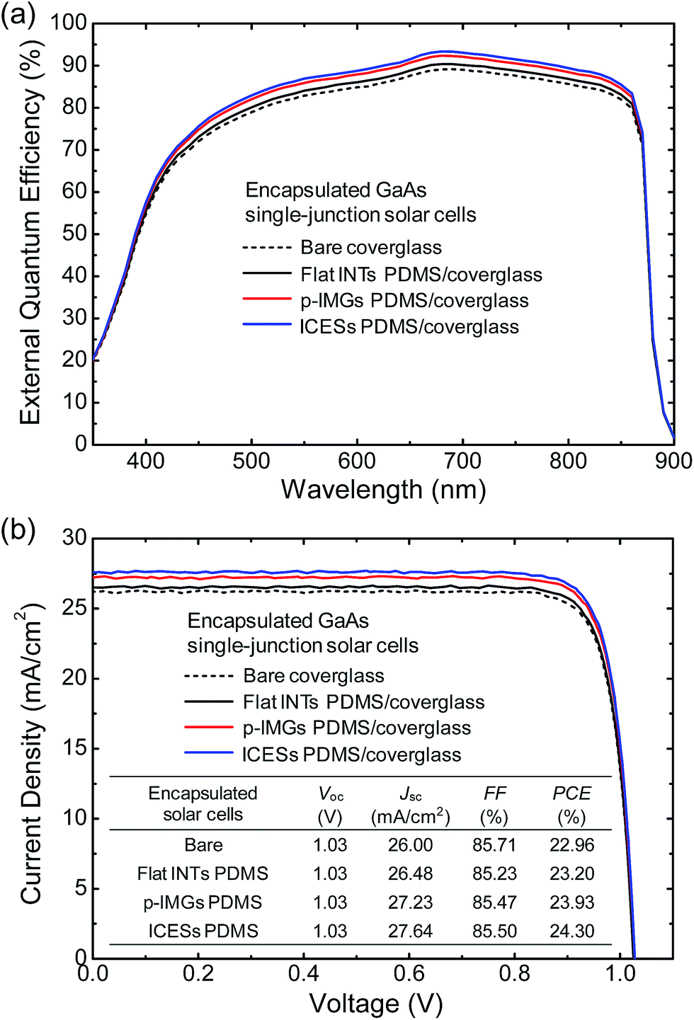
For practical device applications, all the PDMS films were employed onto the coverglass of encapsulated GaAs single-junction solar cells. Fig. 5 shows (a) EQE spectra and (b) current density–voltage (J–V) curves of encapsulated III–V GaAs single-junction solar cells with the flat INTs, the p-IMGs, and the ICESs PDMS films laminated on coverglasses. For comparison, the EQE spectrum and J–V curve of encapsulated III–V GaAs single-junction solar cell with the bare coverglass are also shown in Fig. 5(a) and (b), respectively. The measured device characteristics (i.e., open circuit voltage; Voc, short circuit current density; Jsc, fill factor; FF, PCE) of encapsulated GaAs single-junction solar cells with different antireflection PDMS layers of coverglass are summarized in the inset of Fig. 5(b). As shown in Fig. 5(a), by attaching the PDMS films to the coverglass of encapsulated solar cell devices, the increased EQE spectra were obtained compared to the device with the bare coverglass. The device with the ICESs PDMS/coverglass exhibited improved EQE values compared to the other devices at wavelengths of 400–870 nm due to the larger photogenerated carriers caused by its higher total transmittance and haze properties. As can be seen in Fig. 5(b), compared to the device with the bare coverglass, the use of PDMS films on the coverglass of encapsulated solar cells definitely caused an enhancement of Jsc values while having similar Voc and FF values, and thus it enhanced the PCE of encapsulated solar cells. In particular, for the device with the ICESs PDMS/coverglass, the higher Jsc value of 27.64 mA cm−2 was obtained than that (i.e., Jsc = 26 mA cm−2) of the device with the bare coverglass, as previously demonstrated by EQE measurements. This is attributed to the dramatically increased Havg value of ∼67.6% and SWT value of ∼94.3% over a wide wavelength range of 350–900 nm, which leads to the larger photocurrents due to the enhanced light harvesting in the underneath device cell absorption layer. The increase in Jsc is the main reason of the PCE improvement from 22.96 to 24.3%, indicating the PCE increment percentage of ∼5.8%.
 |
| | Fig. 5 (a) EQE spectra and (b) J–V curves of encapsulated III–V GaAs single-junction solar cells with the flat INTs, the p-IMGs, and the ICESs PDMS films laminated on coverglasses. For comparison, EQE spectrum and J–V curve of encapsulated III–V GaAs single-junction solar cell with the bare coverglass are also shown in (a) and (b), respectively. Measured device characteristics of encapsulated GaAs single-junction solar cells with different antireflection PDMS layers of coverglass are summarized in the inset of (b). | |
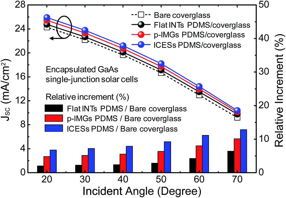
To demonstrate the efficient light-harvesting function (i.e., antireflection and light scattering) of the ICESs PDMS film on the device performance under obliquely incident sunlight, for the corresponding encapsulated III–V GaAs single-junction solar cells, their Jsc values were measured and the increment percentage in Jsc relative to the device with the bare coverglass was estimated at incident angles (θIn) of 20–70°, as shown in Fig. 6. For incident light angle-dependent J–V measurements, inclined mounts with tilting angles of 20–70° were used. As the θIn was increased from 20° to 70°, the Jsc values of all the devices were generally decreased, which shows a similar trend with the other previous reports.11,13,64,65 This is ascribed to the reduction of the projection area where the incident light enters into the device due to the tilted device from the normally incident light source of the solar simulator as well as the increased surface reflection losses.11,65 However, the device with the ICESs PDMS/coverglass showed the higher Jsc value at each θIn, keeping a larger average increment percentage of ∼9.2% relative to the device with the bare coverglass at θIn = 20–70° (i.e., ∼3.4% and ∼6.7% for the flat INTs PDMS/coverglass and the p-IMGs PDMS/coverglass, respectively). Thus, the use of the ICESs DPMS film as an antireflective protective layer could improve the solar power generation in encapsulated photovoltaic systems for an entire day and the seasons.
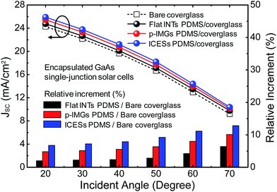 |
| | Fig. 6 Jsc values of the encapsulated III–V GaAs single-junction solar cells with the bare coverglass and the flat INTs, the p-IMGs, and the ICESs PDMS films laminated on coverglasses and estimated increment percentage in Jsc for the devices with the flat INTs, the p-IMGs, and the ICESs PDMS films relative to the device with the bare coverglass at θIn = 20–70°. | |
Self-cleaning effect and stability on device performance under external environment
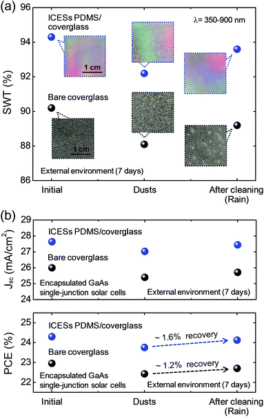
To investigate the self-cleaning function of the ICESs PDMS film on the device performance, the encapsulated solar cells were exposed in outdoor environment. Fig. 7 shows the (a) SWT values of the bare coverglass and the ICESs PDMS/coverglass and (b) Jsc and PCE values of corresponding encapsulated III–V GaAs single-junction solar cells to show the self-cleaning effect. The photographs of the bare coverglass and the ICESs PDMS/coverglass covered by dusts for 7 days under external environment before and after cleaning by falling raindrops are shown in the inset of Fig. 7(a). The samples were mounted on the holder with about 30° tilting angle at the rooftop of a building. For 6 days, there was little rain, and then it rained on the 7th day. As shown in Fig. 7(a), the SWT values of all the samples covered by dusts were reduced from ∼90.2 and ∼94.3% to ∼88.1 and ∼92.2% for the bare coverglass and the ICESs PDMS/coverglass, respectively, because of the interrupting of incident light by the dusts. However, after the cleaning by the falling raindrops, the SWT value of the ICESs PDMS/coverglass was increased by ∼93.6%, exhibiting the larger recovery percentage of approximately 1.6% compared to that (i.e., ∼1.2%) of the bare coverglass (i.e., SWT ≈ 89.2%) in the transmittance. As verified in the photographs of Fig. 7(a), after the cleaning, the dust blotches remained over an entire surface of the bare coverglass while the surface of the ICESs PDMS film was nearly clear due to its self-cleaning effect caused by the hydrophobicity (i.e., θCA ≈ 121°). In Fig. 7(b), similarly, the dusts blocked the incident light into the devices, and thus Jsc values of all the devices were also decreased with a reduction in their PCE values (i.e., from Jsc = 26 and 27.64 mA cm−2 and PCE = 22.96 and 24.3% to Jsc = 25.4 and 27.03 mA cm−2 and PCE = 22.44 and 23.76% for the devices with the bare coverglass and the ICESs PDMS/coverglass, respectively). However, after the cleaning, the Jsc and PCE values of the device with the ICESs PDMS/coverglass were further enhanced to be 27.44 mA cm−2 and 24.13%, respectively, showing a superior PCE recovery percentage of ∼1.6% compared to the device with the bare coverglass (i.e., ∼1.2% recovery percentage, Jsc = 25.71 mA cm−2, PCE = 22.7%). Unlike the Jsc, on the other hand, the Voc and FF values were less influenced by the change of the transmittance due to the dusts.35,48
 |
| | Fig. 7 (a) SWT values of the bare coverglass and the ICESs PDMS/coverglass and (b) Jsc and PCE values of the corresponding encapsulated III–V GaAs single-junction solar cells to show the self-cleaning effect. Photographs of the bare coverglass and the ICESs PDMS/coverglass covered by dusts for 7 days under external environment before and after cleaning by falling raindrops are shown in the inset of (a). | |
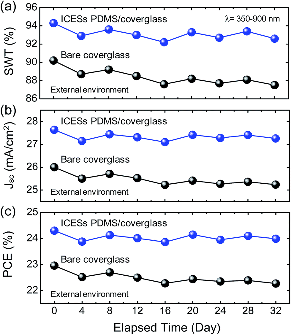
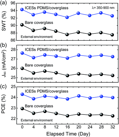
Additionally, to evaluate the self-cleaning function on the long-term device stability of the encapsulated solar cells under external environment, their device performance was further explored for approximately one month. Fig. 8 shows (a) SWT values of the bare coverglass and the ICESs PDMS/coverglass and (b) Jsc values (c) PCE values of the corresponding encapsulated III–V GaAs single-junction solar cells to show the self-cleaning effect for 32 days under external environment. As expected from Fig. 8, the Jsc intensively depended on the SWT, and thus the PCE mainly varied as it. For the device with the bare coverglass, its performance was generally degraded after 32 days with decreasing the SWT, showing the drop percentages of ∼2.9% and ∼3% in Jsc and PCE, respectively, compared to the initial values. On the contrary, owing to the good self-cleaning function of the ICESs PDMS film, the ICESs PDMS/coverglass showed an average increment percentage of ∼5.3% compared to the bare coverglass in the SWT for 32 days. As a result, the device with the ICESs PDMS/coverglass exhibited the superior long-term stability with the lower drop percentages of ∼1.3% and ∼1.4% in Jsc and PCE, respectively.
 |
| | Fig. 8 (a) SWT values of the bare coverglass and the ICESs PDMS/coverglass and (b) Jsc values (c) PCE values of the corresponding encapsulated III–V GaAs single-junction solar cells to show the long-term self-cleaning effect for 32 days under external environment. | |
Conclusions
We fabricated the highly-transparent and hazy ICESs PDMS films with antireflective and hydrophobic properties for efficient light-harvesting and self-cleaning effects for encapsulated III–V GaAs single-junction solar cell applications. The ICESs PDMS film was fabricated by a facile, simple, and cost-effective soft lithography method using sapphire mater molds with CESs consisting of hierarchical NTs/p-MGs. The ICESs PDMS film exhibited larger θCA ≈ 121°, SWT ≈ 94.3%, and Havg ≈ 67.6%, respectively, than those (i.e., θCA ≈ 32°, SWT ≈ 90.2%, and Havg ≈ 4.1%, respectively) of the bare coverglass. By laminating the ICESs PDMS film on the coverglass in the encapsulated III–V GaAs single-junction solar cell, the increased Jsc value of 27.64 mA cm−2 was obtained compared to the encapsulated solar cell with the bare coverglass (i.e., Jsc = 26 mA cm−2), and this mainly enhanced the PCE by 24.3% (i.e., PCE = 22.96% for the encapsulated cell with the bare coverglass), exhibiting the PCE increment percentage of ∼5.8%. Furthermore, it also showed not only superior device performance at obliquely incident lights, but also good long-term device stability with the only PCE drop percentage of ∼1.4% after 32 days. These results suggest that the artificial inverted compound eye structured polymer films, which can be easily fabricated by the simple and cost-effective soft lithography technique, with the high optical transparency and haze as well as the hydrophobic surface have considerable potential for high-performance and long-term stability photovoltaic systems using transparent substrates as well as coverglasses in terms of efficient light-harvesting and self-cleaning functions.
Acknowledgements
This work was supported by the National Research Foundation of Korea (NRF) grant funded by the Korea government (MSIP) (No. 2014-069441). The authors would like to thank the Korea Advanced Nano-Fab Center (KANC) for providing the solar cells.
References
- P. Yu, C. H. Chang, C. H. Chiu, C. S. Yang, J. C. Yu, H. C. Kuo, S. H. Hsu and Y. C. Chang, Adv. Mater., 2009, 21, 1618 CrossRef CAS PubMed.
- J. W. Leem, X. Y. Guan, M. Choi and J. S. Yu, Sol. Energy Mater. Sol. Cells, 2015, 134, 45 CrossRef CAS PubMed.
- D. J. Aiken, Sol. Energy Mater. Sol. Cells, 2000, 64, 393 CrossRef CAS.
- Y. M. Song, Y. Jeong, C. I. Yeo and Y. T. Lee, Opt. Express, 2012, 20, A916 CrossRef PubMed.
- M. A. Green, K. Emery, Y. Hishikawa, W. Warta and E. D. Dunlop, Prog. Photovoltaics, 2014, 22, 1 Search PubMed.
- P. Kuang, J. M. Park, W. Leung, R. C. Mahadevapuram, K. S. Nalwa, T. G. Kim, S. Chaudhary, K. M. Ho and K. Constant, Adv. Mater., 2011, 23, 2469 CrossRef CAS PubMed.
- H. Nagel, A. G. Aberle and R. Hezel, Prog. Photovoltaics, 1999, 7, 245 CAS.
- S. M. Yang, Y. C. Hsieh and C. A. Jeng, J. Vac. Sci. Technol., A, 2009, 27, 336 CAS.
- P. Lalanne and G. M. Morris, Proc. SPIE, 1996, 2776, 300 CrossRef CAS PubMed.
- N. Kadakia, S. Naczas, H. Bakhru and M. Huang, Appl. Phys. Lett., 2010, 97, 191912 CrossRef PubMed.
- C. I. Yeo, H. J. Choi, Y. M. Song, S. J. Kang and Y. T. Lee, J. Mater. Chem. A, 2015, 3, 7235 CAS.
- Y. Nasuno, N. Kohama, K. Nishimura, T. Hayakawa, H. Taniguchi and M. Shimizu, Appl. Phys. Lett., 2006, 88, 071909 CrossRef PubMed.
- J. W. Leem, M. Choi and J. S. Yu, ACS Appl. Mater. Interfaces, 2015, 7, 2349 CAS.
- S. Yang, Y. Wang, L. Bai, B. Liu, J. Fan, X. Yang, H. Zhao, C. Wei, Q. Huang, X. Chen, G. Wang, Y. Zhao and X. Zhang, RSC Adv., 2013, 3, 208 RSC.
- S. Y. Han, C. Pan, D. H. Kim and C. H. Chang, RSC Adv., 2015, 5, 24712 RSC.
- J. W. Leem, Y. M. Song and J. S. Yu, Nanoscale, 2013, 5, 10455 RSC.
- G. Li, J. Li, C. Zhang, Y. Hu, X. Li, J. Chu, W. Huang and D. Wu, ACS Appl. Mater. Interfaces, 2015, 7, 383 CAS.
- R. J. Martín-Palma, C. G. Pantano and A. Lakhtakia, Nanotechnology, 2008, 19, 355704 CrossRef PubMed.
- H. K. Raut, S. S. Dinachali, Y. C. Loke, R. Ganesan, K. K. Ansah-Antwi, A. Góra, E. H. Khoo, V. A. Ganesh, M. S. M. Saifullah and S. Ramakrishna, ACS Nano, 2015, 9, 1305 CrossRef CAS PubMed.
- C. A. Lin, K. Yu Lai, W. C. Lien and J. H. He, Nanoscale, 2012, 4, 6520 RSC.
- C. H. Ho, D. H. Lien, H. C. Chang, C. A. Lin, C. F. Kang, M. K. Hsing, K. Y. Lai and J. H. He, Nanoscale, 2012, 4, 7346 RSC.
- Y. Liu, A. Das, S. Xu, Z. Lin, C. Xu, Z. L. Wang, A. Rohatgi and C. P. Wong, Adv. Energy Mater., 2012, 2, 47 CrossRef PubMed.
- B. Janthong, Y. Moriya, A. Hongsingthong, P. Sichanugrist and M. Konagai, Sol. Energy Mater. Sol. Cells, 2013, 119, 209 CrossRef CAS PubMed.
- Y. H. Ko and J. S. Yu, Opt. Express, 2011, 19, 15574 CrossRef CAS PubMed.
- J. W. Leem, M. S. Kim and J. S. Yu, J. Opt. Soc. Am. B, 2013, 30, 1665 CrossRef CAS.
- Y. P. Chen, C. H. Lee and L. A. Wang, Nanotechnology, 2011, 22, 215303 CrossRef PubMed.
- K. H. Li, C. Feng and H. W. Choi, Appl. Phys. Lett., 2014, 104, 051107 CrossRef PubMed.
- S. H. Huang, R. H. Horng, K. S. Wen, Y. F. Lin, K. W. Yen and D. S. Wuu, IEEE Photonics Technol. Lett., 2006, 18, 2623 CrossRef.
- R. H. Kim, D. H. Kim, J. Xiao, B. H. Kim, S. I. Park, B. Panilaitis, R. Ghaffari, J. Yao, M. Li, Z. Liu, V. Malyarchuk, D. G. Kim, A. P. Le, R. G. Nuzzo, D. L. Kaplan, F. G. Omenetto, Y. Huang, Z. Kang and J. A. Rogers, Nat. Mater., 2010, 9, 929 CrossRef CAS PubMed.
- N. Koo, M. Bender, U. Plachetka, A. Fuchs, T. Wahlbrink, J. Bolten and H. Kurz, Microelectron. Eng., 2007, 84, 904 CrossRef CAS PubMed.
- Y. M. Song, Y. Xie, V. Malyarchuk, J. Xiao, I. Jung, K. J. Choi, Z. Liu, H. Park, C. Lu, R. H. Kim, R. Li, K. B. Crozier, Y. Huang and J. A. Rogers, Nature, 2013, 497, 95 CrossRef CAS PubMed.
- J. W. Leem, S. Kim, S. H. Lee, J. A. Rogers, E. Kim and J. S. Yu, Adv. Energy Mater., 2014, 4, 1301315 Search PubMed.
- J. H. Koschwanez, R. H. Carlson and D. R. Meldrum, PLoS One, 2009, 4, 4572 Search PubMed.
- S. Al-Maawali, J. E. Bemis, B. B. Akhremitchev, R. Leecharoen, B. G. Janesko and G. C. Walker, J. Phys. Chem. B, 2001, 105, 3965 CrossRef CAS.
- Y. B. Park, H. Im, M. Im and Y. K. Choi, J. Mater. Chem., 2011, 21, 633 RSC.
- J. C. Lötters, W. Olthuis, P. H. Veltink and P. Bergveld, J. Micromech. Microeng., 1997, 7, 145 CrossRef.
- Q. Chen, G. Li, Y. Nie, S. H. Yao and J. L. Zhao, Microfluid. Nanofluid., 2014, 16, 83 CrossRef CAS.
- C. J. Ting, F. Y. Chang, C. F. Chen and C. P. Chou, J. Micromech. Microeng., 2008, 18, 075001 CrossRef.
- S. H. Ahn and L. J. Guo, ACS Nano, 2009, 3, 2304 CrossRef CAS PubMed.
- M. A. G. Lazo, R. Teuscher, Y. Leterrier, J. A. E. Månson, C. Calderone, A. Hessler-Wyser, P. Couty, Y. Ziegler and D. Fischer, Sol. Energy Mater. Sol. Cells, 2012, 103, 147 CrossRef PubMed.
- A. B. D. Cassie and S. Baxter, Trans. Faraday Soc., 1944, 40, 546 RSC.
- A. D. Tserepi, M. E. Vlachopoulou and E. Gogolides, Nanotechnology, 2006, 17, 3977 CrossRef CAS.
- K. C. Park, H. J. Choi, C. H. Chang, R. E. Cohen, G. H. McKinley and G. Barbastathis, ACS Nano, 2012, 5, 3789 CrossRef PubMed.
- W. K. Cho and I. S. Choi, Adv. Funct. Mater., 2008, 18, 1089 CrossRef CAS PubMed.
- J. W. Leem and J. S. Yu, Opt. Express, 2012, 20, 26160 CrossRef CAS PubMed.
- T. W. Odom, J. C. Love, D. B. Wolfe, K. E. Paul and G. M. Whitesides, Langmuir, 2002, 18, 5314 CrossRef CAS.
- FullWAVE, RSoft Design Group, http://www.rsoftdesign.com, accessed January 2015.
- J. Son, S. Kundu, L. K. Verma, M. Sakhuja, A. J. Danner, C. S. Bhatia and H. Yang, Sol. Energy Mater. Sol. Cells, 2012, 98, 46 CrossRef CAS PubMed.
- J. W. Leem, D. H. Joo and J. S. Yu, Sol. Energy Mater. Sol. Cells, 2011, 95, 2221 CrossRef CAS PubMed.
- D. G. Stavenga, S. Foletti, G. Palasantzas and K. Arkawa, Proc. R. Soc. London, Ser. B, 2006, 273, 661 CrossRef CAS PubMed.
- Y. M. Song, G. C. Park, S. J. Jang, J. H. Ha, J. S. Yu and Y. T. Lee, Opt. Express, 2011, 19, A157 CrossRef PubMed.
- J. Zhao and M. A. Green, IEEE Trans. Electron Devices, 1991, 38, 1925 CrossRef CAS.
- H. Cui, S. Pillai, P. Campbell and M. Green, Sol. Energy Mater. Sol. Cells, 2013, 109, 233 CrossRef CAS PubMed.
- NREL's Renewable Resource Data Center, http://rredc.nrel.gov/solar/spectra/am1.5, accessed June, 2014.
- J. W. Leem, Y. Yeh and J. S. Yu, Opt. Express, 2012, 20, 4056 CrossRef CAS PubMed.
- Y. Kanamori, H. Kikuta and K. Hane, Jpn. J. Appl. Phys., 2000, 39, L735 CAS.
- Y. M. Song, H. J. Choi, J. S. Yu and Y. T. Lee, Opt. Express, 2010, 18, 13063 CrossRef CAS PubMed.
- W. L. Min, B. Jiang and P. Jiang, Adv. Mater., 2008, 20, 3914 CrossRef CAS PubMed.
- J. H. Shin, K. S. Han and H. Lee, Prog. Photovoltaics, 2011, 19, 339 CAS.
- D. H. Ko, J. R. Tumbleston, K. J. Henderson, L. E. Euliss, J. M. DeSimone, R. Lopez and E. T. Samulski, Soft Matter, 2011, 7, 6404 RSC.
- K. Choi, S. H. Park, Y. M. Song, Y. T. Lee, C. K. Hwangbo, H. Yang and H. S. Lee, Adv. Mater., 2010, 22, 3713 CrossRef CAS PubMed.
- E. Hecht, Optics, Addison-Wesley, NY, USA, 4th edn, 2002, ch. 10 Search PubMed.
- J. W. Leem, Y. M. Song and J. S. Yu, Opt. Express, 2011, 19, 26308 CrossRef CAS PubMed.
- C. H. Chang, M. H. Hsu, P. C. Tseng, P. Yu, W. L. Chang, W. C. Sun and W. C. Hsu, Opt. Express, 2011, 19, A219 CrossRef PubMed.
- Y. M. Song, J. H. Jang, J. C. Lee, E. K. Kang and Y. T. Lee, Sol. Energy Mater. Sol. Cells, 2012, 101, 73 CrossRef CAS PubMed.
Footnote |
| † Electronic supplementary information (ESI) available: SEM images of the thermally dewetted Au nanopatterns for flat sapphire and p-MGs/sapphire, optical measurement system with an integrating sphere, photograph of a water droplet for the flat bare PDMS film, schematic diagram for the water droplet cleaning concept, and photograph of the ICESs PDMS film laminated on the coverglass. See DOI: 10.1039/c5ra05991g |
|
| This journal is © The Royal Society of Chemistry 2015 |
Click here to see how this site uses Cookies. View our privacy policy here. 
 Open Access Article
 This Open Access Article is licensed under a