Anisotropic optical properties of large-scale aligned silver nanowire films via controlled coffee ring effects

Weiping Zhoua, Anming Hu*ab, Shi Baia, Ying Maa and Denzel Bridgesb
aInstitute of Laser Engineering, Beijing University of Technology, 100 Pinle Yuan, Chaoyang District, Beijing 100124, China. E-mail: anminghu@bjut.edu.cn
bDepartment of Mechanical, Aerospace and Biomedical Engineering, University of Tennessee, 1512 Middle Drive, Knoxville, TN 37996, USA

Received 10th March 2015 , Accepted 23rd April 2015

First published on 23rd April 2015


Abstract

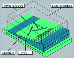
Thin films with one-dimensional nanostructures and unique physical properties are potential candidates for next-generation high-performance electronic, optoelectronic, and electromechanical systems. Here we report that large-scale oriented silver nanowire films can be prepared by controlling the coffee-ring effect through tilting the substrates during the film deposition. The anisotropic optical properties of the orientated silver nanowire film are researched here. Surface enhanced Raman scattering (SERS) spectra were recorded from Rhodamine 6G adsorbed on the silver nanowire films. The SERS spectra showed striking polarization dependence according to the angle between the long axes of the nanowires and the light polarization. At the vertical excitation (i.e., light polarization forms a 90° angle to the long axes of the nanowires), the SERS intensity reaches a maximum. Minimum intensities were obtained at a parallel excitation. The three-dimensional finite element method was used to give an in-depth explanation of these properties. Angular resolution fluorescence is also studied. The fluorescence displays an angle-dependence similar to the Raman activities. Optical properties were also investigated through the polarization of reflectivity spectra. The reflectivity is smaller when the incident light is polarized parallel to the orientation direction. As the wavelength increases, the reflectivity increases when the polarization of incident light is perpendicular to the orientation direction. When the wavelength is greater than 870 nm, the amplitude can be up to doubled. Our study indicates that this technique is promising in the production of large-scale orientated silver nanowire films with anisotropic optical properties for high-performance electronic, optoelectronic, and electromechanical systems.


Introduction

Due to a high surface-to-volume ratio and one dimensional confinement, nanowires show unique optical, magnetic, and electronic properties.1 With the development of nanotechnology, a wide range of low-dimensional nanostructured materials with good quality can now be mass-produced.2–6 However, except through aligned chemical vapor deposition (CVD) growth7 or the Langmuir–Blodgett (LB) technique,8 the preparation of oriented nanowires in a large area is still challenging. The disordered structure in assembled nanowire films is a main limiting factor for the use of device fabrication.9 For photonics and microelectronics,10,11 an ordered structure is needed. Thin films composed of organized one dimensional nanostructures can be potential candidates for next-generation high-performance electronic, optoelectronic, and electromechanical systems.12 Much effort has been placed on developing methods for assembling and positioning the nanowires in desired locations to construct complex, higher-order functional structures.13,14

The Langmuir–Blodgett (LB) technique was traditionally used to align amphiphilic molecule monolayers onto a water surface. Though this technique has been proven to be a versatile and general tool for assembling nanowires or nanorods, there are still some limitations of this method. For example, the surface of hydrophilic nanomaterials must be functionalized with hydrophobic ligands for the LB experiment and the film has to be transferred to the surface of substrates, which greatly restricts their future application.13–15 The evaporation-induced method is one of popular methods for ordered nanostructures,16,17 but the degree of the ordering depend on not only the distribution of nanomaterial's size but also the dewetting of the solvent during the assembly process. It is still challenged to prepare a large area thin film using this method. Based on the interfacial ordering effects, interfaces provide a unique platform for the organization of nanosized building block films in recent years.18,19 But a suitable interface layer is a necessary condition, like the water–oil–air three-phase interface. In the contact-printing method20,21 knocking-down method,22 and strain-release assembly,23 it requires a mechanical force and the auxiliary process for nanowire assembly. In order to obtain ordered structures, physical forces, such as electric fields24 or magnetic fields25 are often employed. These processes often result in localized alignment. We report here a one-step method to prepare large-area ordered silver nanowire films on substrates based on a modified coffee-ring effect.26 Our experimental results show remarkable promise in the production of large-scale ordered nanowire films.

Novel optical properties can be generated by well-aligned Ag nanowires because of the large electromagnetic (EM) fields localized in the interstitial areas of adjacent nanowires.27,28 Importantly, because of the large EM fields, a film with well-aligned Ag nanowires could be used as an excellent Surface enhanced Raman scattering (SERS) substrate for the high sensitivity and selectivity detection of molecules.29,30 The magnitude effect of SERS is not only highly dependent on the excitation conditions and geometry of the metallic nanostructures,31,32 but also strongly dependent on polarization. Only fields polarized along the interparticle axis are enhanced.33 For this study, we fabricated large-scale oriented silver nanowire films and then used them to investigate the polarization-dependent enhancement of SERS and surface enhanced fluorescence (SEF). Also we will investigate the polarization-dependent effect on the reflectivity.

Experimental details

Silver nanowires were prepared according to a reported aqueous method.34,35 Silver nitrate (AgNO3), sodium chloride (NaCl), ethylene glycol (EG), Rhodamine 6G (R6G), and polyvinyl pyrrolidone (PVP, MW = 1[thin space (1/6-em)]300[thin space (1/6-em)]000) were all purchased from Tianjin Fu Chen Chemical Reagents Factory (Tianjin, People's Republic of China). All these reagents, in analytical grade, were used without further purification. The synthesized nanowires were washed using a mixed solution of ethanol and deionized water with the proportion of 1[thin space (1/6-em)]:[thin space (1/6-em)]1 three times. The absorption spectrum of the silver colloid was obtained using a UV-Vis (UV-9000S, Shanghai Metash Instruments Co., Ltd., China) spectrophotometer. The morphology of the silver nanowires was imaged using a scanning electron microscope (SEM; XL30 S-FEG, FEI Co., Hillsboro, OR, USA). The concentration of the silver nanowires solution was increased to 0.5 M by centrifugation. The solution of silver nanowires was poured into a container (the schematic of this device is shown in Fig. 1). The evaporation was carried out inside an oven with fifty degrees Celsius. The deformation occurred at a temperature higher than 50 °C when using plastic substrate. For this method can been used to prepare aligned silver nanowire films in commonly used substrate. So we control the temperature around fifty degrees Celsius. After evaporation of solvent, the self-assembled silver nanowires film was obtained. It takes only about one hour for the evaporation process.
image file: c5ra04214c-f1.tif
Fig. 1 Schematic illustration of silver nanowires self-assembled on silica substrate. Nanowires orderly deposit along the solid–liquid contact line. With the contact line moves inward, the oriented silver nanowires film can be formed.

The silver nanowires films on silicon wafers were used as substrates for SERS, SEF and reflection spectra. Rhodamine 6G was dissolved in water by using ultrasonic cleaning machine for five minutes. The concentrations of the solution were prepared as 1 × 10⁻⁵ M. Then the solution was dropped on the substrate for Raman detection. The SERS and SEF signal were measured with a commercial Raman equipment (inVia-Reflex, Renishaw, Gloucestershire, UK) using a laser with a 532 nm wavelength as the excitation source, the measuring laser spot size was about 3 μm in diameter and the acquisition time was 20 seconds. Three-dimensional finite element method simulation was employed to give an in-depth explanation of SERS properties of these nanowires film samples. Polarization dependent reflectivity spectra were recorded by a commercial angle-resolved spectroscopy.

Results and discussion

Fig. 2 shows the UV-vis absorption spectrum, XRD patterns and SEM image of silver nanowires. UV-vis spectroscopy can be used to detect the morphology of silver nanowires because silver nanostructures having different shapes exhibit SPR bands at different frequencies.36,37 There are two plasmon absorption resonances; one is due to the transverse oscillation of electrons (i.e., electron motion perpendicular to the long axis of the rods or wires) with the peak around 354 nm for silver, approximately coincident with the plasmon of spherical particles, while the second plasmon is due to the oscillation of electrons along the long axis. But as the aspect ratio increases, the longitudinal SPR band will be red-shifted to above 1000 nm, whereas the transverse SPR band shifts to the blue side below 400 nm.38 The peak at 354 nm is due to the transverse plasmon absorption. The broad peak is due to longitudinal plasmon absorption.39 Fig. 2(a) shows a resonant peak at 390 nm and an extended tail from visible to infrared bands. This stands for two contributions from both transverse and longitudinal excitations. Fig. 2(b) shows the XRD pattern of silver nanowires that there are five diffraction peaks, which agree well with the (111), (200), (220), (311), and (222) diffraction of face centered cubic silver. The space group of silver nanowire is Fm[3 with combining macron]m, and the lattice constant calculated from the XRD pattern is 4.085 Å, which is close to the reported data (a = 4.0862 Å, JCPDS file 04-0783).38 Fig. 2(b1) presents a typical SEM image of the silver nanowires. Except for a small number of nanoparticles and nanorods, most of the nanostructures are nanowires. It can be obtained from Fig. 2(c) and (d) that the diameter of the nanowires is around 50 nm, and the length is about 2 microns. The aspect ratio is thus around 40.
image file: c5ra04214c-f2.tif
Fig. 2 The characteristic (a), XRD patterns (b) and SEM image (b1) of silver nanowires. Statistical graph of the diameter (c) and length (d) of nanowires.

Fig. 3 shows SEM images of nanowires films obtained at different deposition conditions. In Fig. 3(c) and (d), it can be clearly seen that the nanowires were deposited with an orientation arrangement. When a drop of nanomaterial solution dries on a solid surface or a liquid–air interface, the nanowires will adopt random orientations and finally leaves dense, well-organized assemblies because of both material–material and material–substrate interactions caused by the coffee ring effect.40 The capillary flow is responsible for the orientation deposition along the contact line, most commonly observed as a coffee ring stain.41 The resulting morphologies and the degree of the ordering achieved vary significantly and depend not only on the nanomaterial's size distribution but also on the directional capillary force, van der Waals attraction and the dewetting of the solvent during the assembly process.42 Rod-shaped nanostructure assembles in a number of ways, such as end-to-end or side-to-side, depending on their concentrations in the dispersions.43,44 Side-to-side assemblies can form ribbon-like structures or smectic arrays. Bates and Frenkel reported two types of phase behaviors for spherocylinders confined to a plane using Monte Carlo simulations.38 According to the result, long rods with aspect ratio >7 behave similar to infinitely thin needles and exhibit a 2D nematic phase at a high density. With the aspect ratio increase to 15–25, 2D bundle structures with occasional side-by-side alignment of bundles into 3D superstructures.45 On the other hand, the resulting outward flow can carry virtually all of the dispersed material to the edge. During drying, liquid evaporating from the edge is replenished by liquid from the interior and the contact line of the droplet undergoes stick-slip motion, that is, small movements interspersed with large and rapid displacements as a result of competition between the pinning and capillary forces. When the contact line is pinned (fixed), the solvent evaporating from the edge is replenished by solvent from the interior. Because the outward solvent flow carries dispersed nanostructures to the edge, the concentration of nanostructures at the edge is higher than that at the center. Owing to the anisotropic nature of the interactions, the tips of the nanowires would be directed along the flow of solution. This explains the self-assembly of rods that are predominantly aligned along the dewetting direction. As a result, the combined effect of the capillary flow and strong interaction leads to the formation of ordered nanowire arrays.46 At the edge of solutions, the contact line pinning and dewetting create the competition between the pinning and depinning forces. During evaporation of solvent, the contact angle decreases and the meniscus interface area increases. These changes cause an increase in a depinning force, without altering the pinning force. When the depinning force reaches a value greater than the pinning force, the contact line starts moving.42 With the solid–liquid contact line moves inward, the oriented silver nanowires film can be formed.


image file: c5ra04214c-f3.tif
Fig. 3 SEM images of nanowires films obtained at different conditions. (a) and (b) obtained by using the nanowire solution directly deposited on the silica surface; (c) and (d) obtained by using the method of controlled coffee ring. Insets in (a) and (c) are photography images of dried films.

Fig. 4 shows the two- and three-dimensional surface profiles of the thin films by either Veeco Surface Profiler or AFM. Fig. 4(a) and (b) shows the morphology features of the thin film at an area of 10 square microns. The surface roughness of arithmetical mean height (Sa) of the film is 545 nm. The root mean square height (Sq) of the film is 650 nm. Veeco Surface Profiler was used to detect the surface morphology at a larger area (Fig. 4(c) and (d)). Quantitative characterization of the surface characteristics shows that the average roughness (Ra) of the film is 419 nm. The root-mean-squared roughness (Rq) of the film is 520 nm. Results obtained from the two methods are close. Quantitative characterization of the film by the two methods demonstrates that the film is very smooth.


image file: c5ra04214c-f4.tif
Fig. 4 Two- and three-dimensional surface profiles of the nanowire film. (a) and (b) obtained by AFM, (c) and (d) obtained by Veeco.

Fig. 5 shows the polarization-dependent SERS spectra of Rhodamine 6G on the Ag nanowires films. The intensity of all the bands in this figure increased as the polarization angle θ changed from 0° to 90°. When the angle approaches 90°, the SERS intensity reaches a maximum. As the angle θ continue to increase, the intensity of all the bands gradually decreases. Minimum intensities were obtained at θ = 0° and θ = 180°. The apparent enhancement factor can be experimentally measured with direct comparison using the following relation: EF = (RSENH/RSREF) × (CREF/CENH), where RSENH and RSREF are the measured Raman intensities, and CREF and CENH are the solution's concentrations for normal and enhanced samples. The film exhibits a cross-section enhancement factor up to 3 × 10⁴ as the polarization angle approaches 90°. It is 4.5 times of that at the parallel condition. To outline this periodicity, the strongest peak located at 611 cm−1 was selected to plot as a function of θ (Fig. 6(a)). It is obvious that the intensity of the Raman band experience fluctuations with respect to θ.


image file: c5ra04214c-f5.tif
Fig. 5 The Raman results of Rhodamine 6G obtained at different angles between polarization and oriented silver nanowires. On the right side shows the schematic diagram of angle.

image file: c5ra04214c-f6.tif
Fig. 6 The intensity of SERS (a) and SEF (b) at the peak of 611 cm−1 obtained at different angles between the linear polarization and oriented nanowires.

The current theoretical understanding of SERS attributes its enhanced intensity to the local electric fields in a confined geometry where the probe molecules are located.47 A strong SERS polarization dependence has also been observed in aligned aggregates of high-aspect-ratio nanowires or nanorods. Unlike the case of isolated nanoparticles, the maximum SERS intensity observed for these assemblies of elongated nanoparticles is in the polarization direction perpendicular to the long axis of the rods/wires.48 Highly localized plasmon modes are created by strong electromagnetic coupling between adjacent metallic nanowires when the polarization direction perpendicular to the long axis of nanowire. So when the angle approaches 90° and 270°, the SERS intensity reaches a maximum.

The polarization effect can be illustrated that the strong and localized enhancement of the EM field possible at favorable locations in systems of interacting nanostructures. In brief, when two nanoparticles close to each other, the optical field in the interstice between them can become enhanced some 6 orders of magnitude above that in the individual particle assuming the exciting illumination is appropriately linearly polarized.44 The origin of the special enhancement obtained when the polarization direction illuminate across the nanowires (or two-nanosphere system) can be understood qualitatively by referring to Fig. 7(a) and (b). In Fig. 7(a), when a molecule located in the interstice is flanked by two sets of conjugate charges arising from the polarization of the individual nanowires, highly localized plasmon modes are created by strong electromagnetic coupling between adjacent metallic nanowires. Contrariwise, when the light is polarized in the other direction illustrated in Fig. 7(b), a molecule in the interstitial region does not benefit from proximity to the induced charges. To further illustrate this effect, the numerical electromagnetic simulations were performed with periodic boundaries (Fig. 7(c) and (d)). The optical material data for silver were taken from Johnson.49 From the Fig. 7(c), the polarization direction perpendicular to the long axis of the nanowires, incident radiation excites a plasmon trapped in the interstitials between cylinders, which lead to SERS enhancements. It correlates well with the predictions by García-Vidal and Pendry, who modeled EM coupling between aligned silver half-cylinders.50 In Fig. 7(d), only in the interstitials that between the ends of the nanowires there is SERS enhancements. Though the maximum enhancements of the ends of the nanowires (in Fig. 7(d)) is twice of the interstitials between cylinders (in Fig. 7(c)), when the polarization direction perpendicular to the long axis of the nanowires, periodic signal enhancement appear on the whole nanowire, and also the area of SERS enhancement is larger than parallel to the nanowires. So the polarization direction perpendicular to the long axis of the Ag nanowires may result in a higher probability of EM enhancements than the parallel polarization.


image file: c5ra04214c-f7.tif
Fig. 7 Simple schematic illustration of the electromagnetic field generated under irradiation, (a) and (b). And the numerical electromagnetic simulations of (c) the polarization direction perpendicular to the long axis of the nanowires, (d) the polarization direction parallel to the long axis of the nanowires.

Raman scattering is an extremely weak nonlinear scattering process. Only when a molecule placed near the metallic nanostructure, Raman cross-sections are much larger than for a molecule in free space. This phenomenon is usually accompanied by SEF as a background.51 However, the research on the enhanced spectroscopy is mostly performed only with the SERS or SEF technique. They are rarely studied together so far. Fig. 5 also shows the enhanced spectra of SEF, which shows a broad based line profile for the fluorescence emission through the whole band. The sharp peaks overlapped on SEF are enhanced resonance Raman signals.47 From our experiment results (Fig. 6(b)), it can be seen that the fluorescent intensity shows the same fluctuation as the Raman signal. This probably indicates that SEF is also based on an EM enhancement mechanism, similar to that of SERS.47

In addition to the Raman and fluorescence properties of the aligned silver nanowire films, optical properties were also investigated through the polarization of reflectivity spectra. Fig. 8(a) shows the reflectivity of nanowires film obtained at different angle. The shapes of the spectra do not show any specific difference with different polarizations. However, the reflectivity is smaller when the incident light is polarized parallel to the oriented direction. It is because that the incident light was absorbed due to the larger dipole-oscillator strength in the parallel direction. This was consistently observed in several samples. Fig. 8(b) is ratio of the reflectivity at 90° to the reflectivity at 0°. It can be seen, as the increase of wavelength, the ratio gradually increased. The plasmon coupling in side-by-side vs. end-to-end dimers of nanorods modeled by discrete dipole approximation method shows an experimental shifts in the optical resonance bands, i.e., red-shift of the longitudinal plasmon band for end-to-end assembly in contrast to the blue-shift for the case of side-by-side assembly.52 So as the increase of wavelength, the reflectivity is larger and larger when the incident light is perpendicularly polarized to the oriented direction. When the wavelength greater than 870 nm, the ratio can be as high as 2.


image file: c5ra04214c-f8.tif
Fig. 8 (a) The reflectivity of nanowires film obtained at different angle. (b) The ratio of reflectivity.

Conclusions

We report that large-scale orientation silver nanowire films can be prepared by controlling the coffee-ring effect through tilting the substrates during the film deposition. The variation tendency of the intensity of all the bands is similar to the sine function, which reaches a maximum at the polarization angle θ = 90° and the minimum intensities were obtained at θ = 0° and θ = 180°. The fluorescent intensity shows the same fluctuation as the Raman signal with respect to the angle θ of incident angle. The reflectivity is smaller when the incident light was polarized parallel to the oriented direction. When the incident light was perpendicularity polarized, the reflectivity was positively associated with the increase of wavelength. Our experiment results indicate that this technique is promising in the production of large-scale orientation silver nanowire films with potential applications in optoelectronic and electromechanical systems.

Competing interests

The authors declare that they have no competing interests.

Author's contributions

Weiping Zhou and Anming Hu conceived of the study and drafted the manuscript. Shi Bai helped with the preparation of silver nanowires. Ying Ma helped with Veeco characterization. Denzel Bridges helped with the modification of this manuscript. All the other works were carried out by Weiping Zhou. All authors read and approved the final manuscript.

Acknowledgements

The study is partially supported by the Beijing oversea High-Level Talent Project and a strategic research grant (KZ20141000500, B-type) of Beijing Natural Science Foundation, P. R. China.

References

  1. R. Z. Li, A. M. Hu and T. Zhang, ACS Appl. Mater. Interfaces, 2014, 6, 21721–21729 CAS.
  2. Y. Xia, P. Yang, Y. Sun, Y. Wu, B. Mayers, B. Gates, Y. Yin, F. Kim and H. Yan, Adv. Mater., 2003, 15, 353–389 CrossRef CAS PubMed.
  3. A. I. Hochbaum and P. D. Yang, Chem. Rev., 2010, 110, 527–546 CrossRef CAS PubMed.
  4. P. D. Yang, R. X. Yan and M. Fardy, Nano Lett., 2010, 10, 1529–1536 CrossRef CAS PubMed.
  5. C. Burda, X. B. Chen and R. Narayanan, Chem. Rev., 2005, 105, 1025–1102 CrossRef CAS PubMed.
  6. S. Bai, W. P. Zhou, Y. H. Lin, Y. Zhao, T. Chen, A. M. Hu and W. W. Duley, J. Nanopart. Res., 2014, 16, 2470 CrossRef.
  7. O. Dag, G. A. Ozin and H. Yang, Adv. Mater., 1999, 11, 474–480 CrossRef CAS.
  8. F. Kim, S. Kwan and J. Akana, J. Am. Chem. Soc., 2001, 123, 4360–4361 CrossRef CAS.
  9. S. Bai, W. P. Zhou and T. Chen, Curr. Nanosci., 2014, 10, 486–496 CrossRef CAS.
  10. G. H. Yu and C. M. Lieber, Pure Appl. Chem., 2010, 82, 2295–2314 CAS.
  11. W. Lu and C. M. Lieber, Nat. Mater., 2007, 6, 841–850 CrossRef CAS PubMed.
  12. K. J. Ziegler, B. Polyakov, J. S. Kulkarni, T. A. Crowley, K. M. Ryan, M. A. Morris, D. Erts and J. D. Holmes, J. Mater. Chem., 2004, 14, 585 RSC.
  13. A. R. Tao, J. X. Huang and P. D. Yand, Acc. Chem. Res., 2008, 41, 1662–1673 CrossRef CAS PubMed.
  14. L. Jiang, H. L. Dong and W. P. Hu, Soft Matter, 2011, 7, 1615–1630 RSC.
  15. S. Acharya, J. P. Hill and K. Ariga, Adv. Mater., 2009, 21, 2959–2981 CrossRef CAS PubMed.
  16. C. Y. Zhang, X. J. Zhang, X. H. Zhang, X. Fan, J. S. Jie, J. C. Chang, C. S. Lee, W. J. Zhang and S. T. Lee, Adv. Mater., 2008, 20, 1716 CrossRef CAS PubMed.
  17. J. H. Wu, T. Z. Xu, S. G. Ang, Q. H. Xu and G. Q. Xu, Nanoscale, 2011, 3, 1855–1860 RSC.
  18. R. Hara, T. Fukuoka, R. Takahashi, Y. Utsumi and A. Yamaguchi, RSC Adv., 2014, 5, 1378 RSC.
  19. H. M. Ma and J. C. Hao, Chem. Soc. Rev., 2011, 40, 5457–5471 RSC.
  20. A. Javey, S. Nam, R. S. Friedman, H. Yan and C. M. Lieber, Nano Lett., 2007, 7, 773–777 CrossRef CAS PubMed.
  21. Z. Y. Fan, J. C. Ho, Z. A. Jacobson, R. Yerushalmi, R. L. Alley, H. Razavi and A. Javey, Nano Lett., 2008, 8, 20–25 CrossRef CAS PubMed.
  22. A. Pevzner, et al., Nano Lett., 2010, 10, 1202–1208 CrossRef CAS PubMed.
  23. F. Xu, J. W. Durham, B. J. Wiley and Y. Zhu, ACS Nano, 2011, 5, 1556–1563 CrossRef CAS PubMed.
  24. J. K. Kawasaki and C. B. Arnold, Nano Lett., 2011, 11, 781–785 CrossRef CAS PubMed.
  25. B. Wang, Y. F. Ma, N. Li, Y. P. Wu, F. F. Li and Y. S. Chen, Adv. Mater., 2010, 22, 3067–3070 CrossRef CAS PubMed.
  26. W. P. Zhou, A. M. Hu, S. Bai, Y. Ma and Q. S. Su, Nanoscale Res. Lett., 2014, 9, 87 CrossRef PubMed.
  27. S. J. Liu, C. L. Jiang, B. Yang, Z. P. Zhang and M. Y. Han, RSC Adv., 2014, 4, 42358 RSC.
  28. J. W. Liu, H. W. Liang and S. H. Yu, Chem. Rev., 2012, 112, 4770–4799 CrossRef CAS PubMed.
  29. L. B. Yang, P. Li and J. H. Liu, RSC Adv., 2014, 4, 49635 RSC.
  30. X. C. Sun, S. Stagon, H. C. Huang, J. Chen and Y. Lei, RSC Adv., 2014, 4, 23382 RSC.
  31. A. G. Brolo, E. Arctander and C. J. Addision, J. Phys. Chem. B, 2005, 109, 401–405 CrossRef CAS PubMed.
  32. A. Hu, Q. B. Lu, W. W. Duley and M. Rybachuk, J. Chem. Phys., 2007, 126, 154705 CrossRef CAS PubMed.
  33. D. H. Jeong, Y. X. Zhang and M. Moskovits, J. Phys. Chem. C, 2004, 108, 12724–12728 CrossRef CAS.
  34. Y. J. Song, M. L. Wang, X. Y. Zhang, J. Y. Wu and T. Zhang, Nanoscale Res. Lett., 2014, 9, 17 CrossRef PubMed.
  35. P. Peng, A. M. Hu, B. X. Zhao, A. P. Gerlich and Y. N. Zhou, J. Mater. Sci., 2012, 47, 6801–6811 CrossRef CAS.
  36. M. Kerker, J. Colloid Interface Sci., 1985, 105, 297–314 CrossRef CAS.
  37. D. Sarkar and N. J. Halas, Phys. Rev. E: Stat. Phys., Plasmas, Fluids, Relat. Interdiscip. Top., 1997, 56, 1102–1112 CrossRef CAS.
  38. M. A. Bates and D. J. Frenkel, J. Chem. Phys., 2000, 112, 10034 CrossRef CAS PubMed.
  39. M. N'Gom, R. Jan, F. M. John, A. Ashish, K. Nicholas, J. Z. Nestor and B. N. Theodore, Nano Lett., 2008, 8, 3200–3204 CrossRef PubMed.
  40. X. M. Lin, H. M. Jaeger, C. M. Sorensen and K. J. Klabunde, J. Phys. Chem. B, 2001, 105, 3353–3357 CrossRef CAS.
  41. A. R. Tao, J. X. Huang and P. D. Yang, Acc. Chem. Res., 2008, 41, 1662–1673 CrossRef CAS PubMed.
  42. F. Kim, S. Kwan, J. Akana and P. D. Yang, J. Am. Chem. Soc., 2001, 123, 4360–4361 CrossRef CAS.
  43. P. Narayan and S. Efrima, J. Phys. Chem. B, 2004, 108, 11964–11970 CrossRef.
  44. T. K. Sau and C. J. Murphy, Langmuir, 2005, 21, 2923–2929 CrossRef CAS PubMed.
  45. R. Nikhil and D. Jana, Angew. Chem., Int. Ed., 2004, 43, 1536–1540 CrossRef PubMed.
  46. C. Y. Zhang, X. J. Zhang, X. H. Zhang, X. Fan, J. S. Jie, J. C. Chang, C. S. Lee, W. J. Zhang and S. T. Lee, Adv. Mater., 2008, 20, 1716–1720 CrossRef CAS PubMed.
  47. Y. P. Zhao, S. B. Chaney, S. Shanmukh and R. A. Dluhy, J. Phys. Chem. B, 2006, 110, 3153–3157 CrossRef CAS PubMed.
  48. D. H. Jeong, Y. X. Zhang and M. Moskovits, J. Phys. Chem. B, 2004, 108, 12724–12728 CrossRef CAS.
  49. P. B. Johnson and R. W. Christy, Phys. Rev. B: Solid State, 1972, 6, 4370–4379 CrossRef CAS.
  50. F. J. García-Vidal and J. B. Pendry, Phys. Rev. Lett., 1996, 77, 1163 CrossRef.
  51. J. Dong, S. X. Qu, H. R. Zheng, Z. L. Zhang, J. N. Li, Y. P. Huo and G. A. Li, Sens. Actuators, B, 2014, 191, 595–599 CrossRef CAS PubMed.
  52. P. K. Jain, S. Eustis and M. A. El-Sayed, J. Phys. Chem. B, 2006, 110, 18243–18253 CrossRef CAS PubMed.

This journal is © The Royal Society of Chemistry 2015
Click here to see how this site uses Cookies. View our privacy policy here.