
 Open Access Article
 This Open Access Article is licensed under a
 Creative Commons Attribution 3.0 Unported Licence
Solution processed graphene–silicon Schottky junction solar cells
Lachlan J.
Larsen
,
Cameron J.
Shearer
,
Amanda V.
Ellis
and
Joseph G.
Shapter
*
Flinders Centre for NanoScale Science and Technology, School of Chemical and Physical Sciences, Flinders University, Bedford Park, GPO Box 2100, Adelaide, SA 5001, Australia. E-mail: joe.shapter@flinders.edu.au
First published on 20th April 2015
Abstract
Here, surfactant-assisted exfoliated graphene (SAEG) has been used to make transparent conducting graphene films which for the first time were used to make SAEG–silicon Schottky junctions for photovoltaics. The graphene films were characterised using UV-Vis spectroscopy, Raman spectroscopy, atomic force microscopy and four point probe sheet resistance measurements. The effects of film thickness, thermal annealing and chemical doping of the graphene films on the power conversion efficiency (PCE) of the cells were investigated. Mild annealing of thickness optimised films resulted in a doubling of the PCE. Additionally, chemical doping resulted in a further 300% increase of the peak PCE. These results indicate that SAEG has the potential to compete with chemical vapour deposited graphene in graphene–silicon Schottky junction applications.
Introduction
In the last decade nanocarbon–silicon heterojunctions have been investigated for their photovoltaic properties, specifically carbon nanotube–silicon (CNT–Si)1 and graphene–silicon (G–Si).2 Wei et al.3 were the first to report a CNT–Si heterojunction in 2007. They used chemical vapour deposition (CVD) to grow a double-walled carbon nanotube film, after which the film was suspended in distilled water and picked up on a pre-patterned n-type silicon substrate to create a p(CNT)–n(Si) junction. Their work has been expanded on by numerous researchers using a myriad of different nanotubes,4,5 architectures6,7 and dopants.8,9 The mechanism by which these CNT–Si heterojunctions function, whether they are Schottky or p–n junctions, is currently under debate, however, it is clear that the CNTs have a twofold role in these architectures. Importantly, the CNTs act as transparent conducting electrodes, transporting holes. However, these holes are generated as a result of charge separation at the CNT–Si interface, in which the CNTs are an active layer.Graphene in G–Si heterojunctions also has a two-fold role, similar to CNTs, although it is widely accepted that these heterojunctions are purely Schottky in nature.2 While a detailed description has been previously reported,10 in brief, when semiconducting n-type silicon is in contact with metallic graphene a Schottky junction is formed. Upon illumination electron–hole pairs are photoexcited in the silicon and separated due to the built in potential at the interface. The graphene layer acts as a transparent conductive electrode transporting holes from the Si. The first report on G–Si heterojunctions was published by Li et al.,10 who used CVD graphene with n-type silicon to produce Schottky junctions with power conversion efficiencies (PCE) of up to 1.3% under AM1.5 illumination. These cells showed good stability, retaining their performance over a two month period.
Since the seminal work of Li et al.,10 there have been a number of advances made to the PCE of G–Si Schottky junctions. These include changing the silicon at the interface from planar to nanowire or nanohole arrays11–13 as well as changing the number of layers of CVD graphene present.14–16 However, the majority of research has focused on chemical doping methods.17 The first to report doping of G–Si Schottky junctions in a photovoltaic application were Fan et al.11 who used thionyl chloride (SOCl2) to dope G–Si nanowire Schottky junctions. The SOCl2 doping increased the PCE from 0.68% to 2.86% after increases to the short circuit current density (JSC), open circuit voltage (VOC) and fill factor (FF) of the cells.11 Interestingly, while the VOC remained stable after doping, the JSC and FF decreased over a period of two weeks before plateauing at a stable PCE of ∼1.2%. Following this result, a number of different dopants have been investigated including nitric acid,13,16,18,19 poly(3,4-ethylenedioxythiophene):polystyrene sulfonate (PEDOT:PSS),18 bis(trifluoromethanesulfonyl)amide,20 and gold chloride.19 Chemical doping methods have also recently been combined with colloidal antireflection layers21,22 with a recent record PCE of 15.6% set by Song et al.22 These examples highlight the interest in G–Si Schottky junctions but are limited in their scale up potential due to the use of graphene produced by CVD, which is both expensive and difficult to synthesise in large quantities. These properties of the CVD process limit its use in the industrial setting and cast doubt on whether such approaches could be used to economically produce commercial solar cells.
The most common procedure to produce single layer graphene in large quantities is the oxidation and sonochemical exfoliation of graphite into graphene oxide (GO) by the modified Hummers method.23,24 Oxidation is essential in order to facilitate exfoliation but severely disrupts sp2 hybridisation and subsequently reduces conductivity and mechanical stability. Thermal or chemical reduction (to produce rGO) is not capable of sufficiently repairing the damage of oxidation. GO/rGO–Si Schottky junction solar cells have been investigated by a number of groups with PCE values from 0.02–0.3% reported.25–28 The fabricated cells typically display low short circuit current density and poor fill-factors which result from poor hole mobility in the GO (or rGO) layer.
In order to produce large quantities of graphene without prior oxidation Blake et al.29 and Hernandez et al.30 developed a method of top-down graphene production using solvent-assisted exfoliation of bulk graphite to produce graphene without the need for CVD and in higher yield than mechanical scotch tape exfoliation, first used in the isolation of graphene.31,32 This solvent-assisted exfoliation method was expanded upon by numerous research groups in order to increase the concentration and quality of the graphene flakes produced. This was achieved through the investigation of numerous types of organic solvents,33–35 ultrasonication times36 and introducing filtration and filtrate re-suspension.37 While these methods succeeded in producing single- and few-layer graphene dispersions, they were limited in their application due to the presence of difficult to process organic solvents, which are typically toxic, have a high boiling point or both.
In order to mitigate the use of organic solvents Lotya et al.38 reported a method for the liquid phase exfoliation of graphite in the absence of organic solvents. Using the common ionic surfactant sodium dodecylbenzene sulfonate (SDBS) they produced graphene dispersions at a concentration of up to 0.05 mg mL−1. Although a number of different studies have been conducted using ionic surfactant-assisted exfoliation, for example,39,40 Guardia et al.41 showed that non-ionic surfactants outperformed ionic surfactants in making high concentration graphene dispersions when the surfactant concentrations were not optimised. Indeed, using the non-ionic surfactants Tween-80 and P-123 graphene concentrations of 0.5–1 mg mL−1 were achieved. Solution and surfactant-assisted exfoliation of graphene have the advantage over oxidation-assisted exfoliation, used to prepare graphene oxide, in that the basal planes of graphene remain pristine and thus retain their intrinsic mechanical and electrical properties.30
Recently, work has been directed towards using liquid phase exfoliated graphene and similar 2D materials in inkjet printers for numerous electronic devices.42,43 Despite the existence of a simple method for few-layer graphene production and hence the ability to produce easily transferrable transparent, conducting graphene films, to the best of the authors' knowledge, surfactant-assisted exfoliated graphene has thus far not been investigated in G–Si Schottky junctions for photovoltaics. Here, we present a method for producing G–Si Schottky junctions from surfactant-assisted exfoliated graphene and investigate the effects of both film thickness and chemical doping on the photovoltaic properties of the heterojunctions.
Experimental methods
Graphene film fabrication
Flake graphite (+100 mesh, Sigma Aldrich, Australia) was ultrasonicated (Elmasonic ElmaS30H, 80 W) in an aqueous Tween-60 solution (1% v/v, Sigma Aldrich, Australia) at a concentration of 0.1 g mL−1 for 2 h. Ultrasonication was halted every 15 min and the sample stirred with a magnetic stirrer to improve dispersion. The black dispersion was then centrifuged at 1400 rcf (3200 rpm) for 10 min and the supernatant removed via pipette.Graphene films with an area of 0.18 cm2 were prepared for device fabrication while an area of 0.50 cm2 was used for all other measurements. To form graphene films, the supernatant was filtered through mixed cellulose ester (MCE) membranes (0.45 μm, HAWP, Millipore, USA). The UV-Vis transmittance at 550 nm of the resultant graphene films can be controlled by varying the volume of graphene dispersion (mL) filtered per unit area of the final film (cm−2). The amount of supernatant used to produce each film was such that transmittances of 13% T to 76% T were produced for each purpose (sheet resistance measurements or solar cells etc.). These films were then rinsed thoroughly with deionised water before their application.
Solar cell fabrication
See Fig. 1 for a cutaway schematic of the final cell architecture. Phosphorous doped n-type silicon wafers (CZ, 1–20 Ω cm, 〈100〉, ABC GmbH, Germany), polished on one side and with a 100 nm thermal oxide layer were used for device fabrication. UV lithography was used to define circular holes (area of 0.08 cm2) in the sputtered front metal contacts (Ti/Au 5 nm/145 nm) which were then used as a mask for buffered oxide etching (BOE) (6![[thin space (1/6-em)]](https://www.rsc.org/images/entities/char_2009.gif) :1 40% NH4F:49% HF) of the oxide layer. Graphene films were then deposited by placing the circular graphene–MCE membranes graphene side down over the etched hole. The membranes were then wetted with deionised water and a Teflon sheet placed on top of the membrane. The assembly was then compressed with a glass slide and baked at 80 °C for 15 min. The assembly was then allowed to cool and subsequently immersed in acetone to dissolve the MCE, leaving a tightly physisorbed graphene membrane on the silicon/gold substrate. The oxide layer on the back of the silicon was then etched using BOE and an electrical contact was made between the silicon and a stainless steel back electrode using eutectic gallium indium (eGaIn, Sigma-Aldrich, Australia), consistent with the work of Tune et al. in their CNT–Si heterojunction cells.1,5–7
:1 40% NH4F:49% HF) of the oxide layer. Graphene films were then deposited by placing the circular graphene–MCE membranes graphene side down over the etched hole. The membranes were then wetted with deionised water and a Teflon sheet placed on top of the membrane. The assembly was then compressed with a glass slide and baked at 80 °C for 15 min. The assembly was then allowed to cool and subsequently immersed in acetone to dissolve the MCE, leaving a tightly physisorbed graphene membrane on the silicon/gold substrate. The oxide layer on the back of the silicon was then etched using BOE and an electrical contact was made between the silicon and a stainless steel back electrode using eutectic gallium indium (eGaIn, Sigma-Aldrich, Australia), consistent with the work of Tune et al. in their CNT–Si heterojunction cells.1,5–7
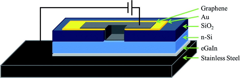 | ||
| Fig. 1 Cutaway schematic of the G–Si Schottky junction architecture used. | ||
Doping of solar cells
Cells were doped with nitric acid (70%, Sigma-Aldrich, Australia) by exposing them to concentrated nitric acid vapour for 2 min. Alternatively, cells were doped with gold chloride (99%, Aldrich, Australia) by dynamic spin coating (30 s at 3000 rpm) of AuCl3 dissolved in ethyl ether (10 mM).Characterisation
UV-Visible spectra of graphene films on glass slides (deposited analogously to the previously described film deposition on silicon) were taken with a resolution of 1 nm using a Varian Cary 50G spectrophotometer. Raman spectra were collected with a WITec alpha300R microscope using a 40× objective (NA 0.9) and a 532 nm laser operating at constant power for each spectrum up to a possible maximum of 60 mW. Raman spectra were collected with an integration time of 6 s and 10 accumulations. Sheet resistance measurements were taken from graphene films on glass using a four-point probe (KeithLink) in linear geometry and a multimeter (GDM-8261, GW Instek). AFM images were acquired in air using a Bruker Dimension FastScan AFM with Nanoscope V controller, operating in tapping mode. Silicon cantilevers (MikroMasch) with a fundamental resonance frequency of between 300 and 400 kHz were used. Images were obtained using a scan rate of 1 Hz with the set point, amplitude, and feedback control parameters optimised manually for each sample. The images presented have been flattened using NanoScope Analysis v1.4 software.Film annealing
Annealed films for sheet resistance were prepared by annealing the graphene films on glass in a tube furnace at 250 °C under a forming gas atmosphere (1:20 H2:Ar) for 2 h. Annealed cells were prepared by annealing G–Si substrates prior to back BOE etching in the same tube furnace conditions.
Solar testing
After cell assembly, the G–Si interface was treated with 2% HF (diluted from 48%, Sigma-Aldrich, Australia) to remove any native oxide layer that had grown back on the Si during the assembly process, and the first J–V test after this step was denoted as the 0 h test. Current–voltage data was collected using a Keithley 2400 SMU instrument and recorded using a custom LabView Virtual Instrument program. Cells were illuminated by collimated 100 mW cm−2 light from a xenon-arc source passed through an AM1.5G filter with the irradiance at the sample plane being measured with a silicon reference cell (PV Measurements, NIST-traceable calibration). J–V curves were obtained by scanning from 1 to −1 V.Results and discussion
Graphene characterisation
Aqueous graphene dispersions were prepared using the non-ionic surfactant Tween-60, following a modified version of the Guardia et al. method.41 These dispersions were found to have an extinction coefficient of 2574 mL mg−1 m−1 at 660 nm and an average concentration of 0.1 mg mL−1. Fig. 2(a) shows the Raman spectrum of both the pristine graphite flakes used to prepare the dispersion and a graphene film deposited on glass. The Raman spectrum of the graphene film exhibits a 2D peak shifted to a lower wavenumber (2709 cm−1 for graphite and 2691 cm−1 for the graphene film). This shift, along with the disappearance of the characteristic graphite 2D shoulder (at 2685 cm−1) and a broadening of the peak indicates the majority presence of few-layer graphene (FLG) flakes in the dispersion44 as well as providing evidence that the graphene flakes do not restack in an AB pattern when being deposited in a film.45 UV-Vis of the films (Fig. 2(b)) also shows the expected featureless absorption spectrum across the visible range characteristic of surfactant exfoliated graphene.38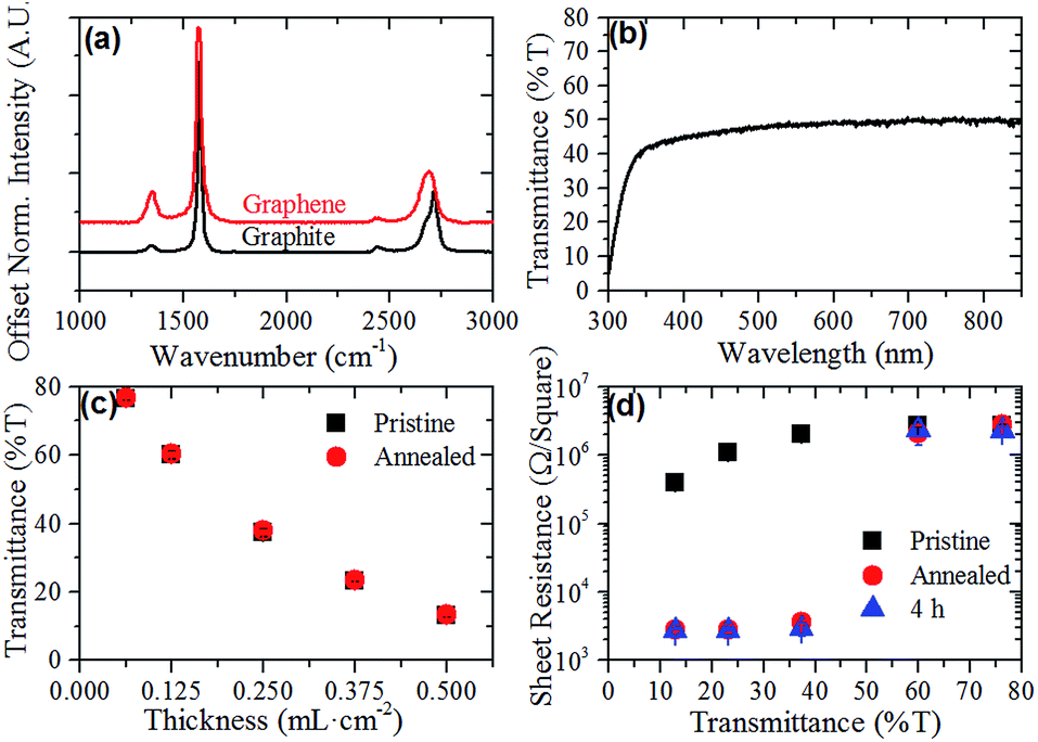 | ||
| Fig. 2 (a) Normalised Raman spectra of graphite flakes (black) and a graphene film deposited on glass (red), (b) representative UV-Vis spectrum of a graphene film on glass, (c) UV-Vis transmittance at 550 nm of pristine (squares) and annealed (circles) graphene films of varying thicknesses on glass and (d) sheet resistance of graphene films of varying thickness on glass measured pristine, after annealing in forming gas for 2 h and then 4 h after annealing. Error bars are present in (c) and (d) but lie within the series symbol for the majority of points. | ||
By controlling the volume of graphene dispersion filtered per unit area of the MCE membrane, the optical thickness of the films could be controlled. Fig. 2(c) shows the volume per unit area (mL cm−2) versus the UV-Vis transmittance of the films at 550 nm. The transmittance of the graphene films at 550 nm was found to decrease nonlinearly with increased volume of graphene dispersion used for the preparation of the films. This non-linear behavior suggests that there is a limit to the thickness of the graphene films using this deposition method, as the UV-Vis transmittance should scale linearly with an increasing number of graphene layers. This limit may arise due to the weight of the thicker films embedding the bottom graphene flakes more strongly into the MCE filters, causing these flakes to be washed away during the film's removal. However, the relationship between volume filtered and UV-Vis transmittance showed reasonable reproducibility, as evidenced by the standard deviations shown in Fig. 2(c). Upon thermal annealing, the films showed no change in transmittance at 550 nm (Fig. 2(c)).
Fig. 2(d) shows the average sheet resistance of the graphene films of varying thickness in their pristine and annealed conditions. As expected the thickness of the graphene films significantly effects their sheet resistance, with the thickest 13% T films having a drop in their sheet resistance of almost an order of magnitude compared to the 76% T films ((4.0 ± 0.2) × 106 Ω □−1 and (2.7 ± 0.2) × 105 Ω □−1, respectively). The sheet resistance of the pristine films appears to show two regimes within the films, a thin film regime and a thick film regime. While the sheet resistance of the two thinnest films is the same within experimental error, the three thicker films show decreasing sheet resistance with increasing thickness. These two regimes were much more prominent when the sheet resistance of the films was measured again post annealing. As Fig. 2(d) shows, the sheet resistance of the thinner 76% T and 60% T films remained constant, within experimental error, while there was a nearly three orders of magnitude decrease in sheet resistance for the thicker films, with the 23% T film showing the best performance at (2.8 ± 0.3) × 103 Ω □−1. These sheet resistances compare favorably with other surfactant-assisted exfoliated graphene films such as those by Lotya et al.38 (higher sheet resistance but higher transparency), De et al.46 (comparable sheet resistance and transmittance but annealed at 500 °C) and Guardia et al.41 (lower conductivities with opaque films).
It is hypothesised that there are two contributing factors to the changes in sheet resistance observed in the pristine and annealed films. The first difference between the two regimes is that the thin films are largely incomplete films, with graphene flakes acting as islands along the length of the film. Thus, electrons are unable to travel directly between flakes across large distances and must instead follow a hopping mechanism, increasing the sheet resistance of the films.
The film formation was observed by performing AFM on both the 76% T and 23% T films that were deposited on silicon substrates, seen in Fig. 3(a)–(c). Comparison of a 5 × 5 μm area on a 76% T film (Fig. 3(a)) and a 10 × 10 μm area on a 23% T film (Fig. 3(c)) shows a clear difference between the film morphologies on both lateral and vertical dimensions. Fig. 3(a) shows several few-layer (and thicker) graphene flakes spread across the imaged area. Fig. 3(b) shows a 1 × 1 μm zoom in of one of the few-layer flake seen in Fig. 3(a) with the corresponding cross sections presented in Fig. 3(d), showing an average flake thickness of 6.4 nm. This flake and others can be seen spread out from each other with the silicon substrate beneath clearly visible. Fig. 3(c), however, shows a very densely packed film with no apparent silicon substrate visible underneath, with a greater maximum height scale of 400 nm.
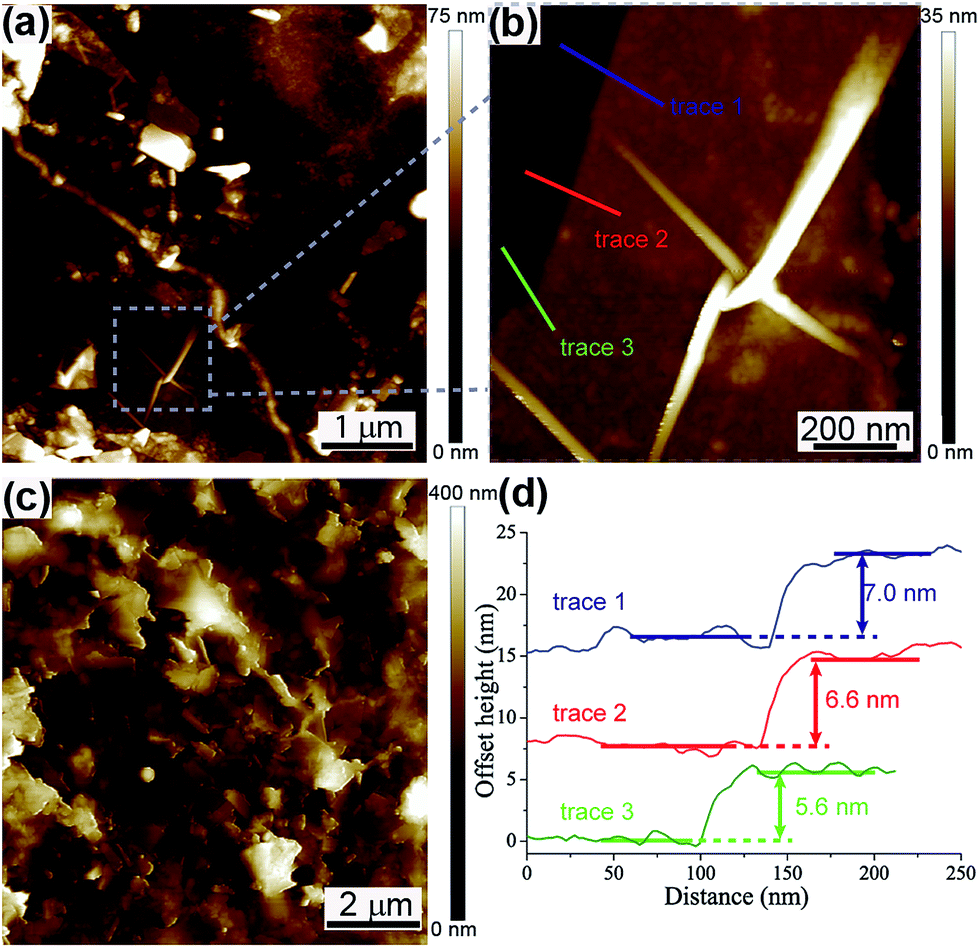 | ||
| Fig. 3 Representative AFM images of (a) 5 × 5 μm area of a 76% T film on silicon substrate, (b) a zoom in on a 1 × 1 μm area showing an exfoliated graphene flake exhibiting characteristic wrinkling, (c) a 10 × 10 μm area of a 23% T film on a silicon substrate, and (d) trace heights of the graphene flake seen in (b) showing an average height of 6.4 nm. | ||
The second difference between the films arises from the film production method. In order to ensure consistent film production, all films were prepared by diluting the volume of stock solution for the required thickness of the film in 1 L of water. It was therefore expected that the thinner films would have inherently less residual surfactant as the solution would be more dilute before filtering. Despite rinsing with copious amounts of water, the thicker films could still have more residual insulating surfactant between the graphene flakes, and hence a higher sheet resistance. When the films are then annealed, this residual surfactant decomposed and the graphene flakes were brought into better electrical contact with each other resulting in lower sheet resistances, with Fig. 2(d) showing that this decrease in sheet resistance is stable at least 4 h after the annealing treatment.
Photovoltaic characterisation
The PCE of the cells made using varying thicknesses of graphene films are displayed in Fig. 4(a). Fig. 4(b) shows the maximum PCE achieved by the cells with respect to their film thickness. The bimodal nature of Fig. 4(b) suggests that there are two film thickness regimes, in line with the sheet resistance of the films (Fig. 2(d)). Interestingly, cells of all film thicknesses were found to have a time dependence related to the HF etching of the front junction (Fig. 4(a)). This time dependence was most marked in the first 48 h after etching but began to plateau after approximately 150 h. This extended time dependence is proposed to be due to the gradual regrowth of oxide layer at the interface of the graphene film and the n-type silicon. The impermeability of graphene47 means that the interface's exposure to oxygen to regrow the oxide is reduced compared to other systems such as the CNT–silicon interface.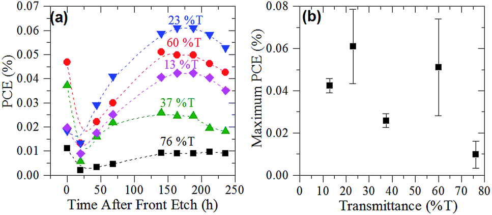 | ||
| Fig. 4 (a) PCE of G–Si cells of varying graphene film thickness measured after back and front etching (lines added to aid the eye) and (b) maximum efficiency of G–Si cells after back and front etching as a function of graphene film thickness. | ||
The maximum PCE found for the pristine cells was 0.06%, at a film thickness of 23% T. This PCE was achieved with a JSC of 0.68 mA cm−2, VOC of 0.41 V and a fill factor of 0.21. This PCE was low compared with the first CVD G–Si Schottky junction by Li et al.,10 however, agreement between the cell's VOC was quite good (at 0.42–0.48 V for CVD cf. 0.41 V). This is further proof that the aqueous graphene dispersions are indeed few-layer graphene.
As the sheet resistance of the thicker graphene films was greatly reduced after annealing, two sets of G–Si cells were prepared to investigate the effect of annealing the graphene film on the photovoltaic performance of the G–Si cells. The thin (60% T) and thick films (23% T) with the best photovoltaic performance, as shown in Fig. 4(b), were prepared as per normal methodology. Before the back etch step, the cells were annealed under the same conditions as the films on glass used for sheet resistance measurements. Once the cells were annealed they were back and front etched following the pre-established protocol. Fig. 5(a) shows the PCE of the annealed cells after back and front etching. Comparison of Fig. 4(a) and 5(a) shows that the same time dependent trend of cell PCE observed in pristine film cells is also observed in the annealed film cells. More importantly, while the thin film performance has been slightly reduced when compared to the pristine cells, the thicker 23% T film cells show an improvement in PCE of 50% even upon initial testing, which rose to over 100% over the course of 3 days (0.06–0.13%). The representative J–V curves of the 23% T film are shown in Fig. 5(b). These results show that the observed increase in the PCE of the cells was due mainly to the increase in the average JSC of the cells (a 200% increase compared with pristine cells), with a 35% increase in average FF and no change in average VOC when compared to the pristine cells. The increase in JSC of the cells is in line with the observed decrease in sheet resistance of the annealed films in Fig. 2(d). As the sheet resistance of the films was decreased, due to the loss of residual surfactant, it is easier for holes to be transported from the graphene–silicon interface through the graphene to the front electrode and hence the measured JSC is increased. This loss of residual surfactant also resulted in a slight increase in FF, as there was less recombination due to surfactant. As the annealing does not result in the knitting together of graphene flakes, there are still a large number of recombination sites within the graphene sheet suppressing the FF. This simple annealing step further improved the JSC in comparison to early CVD G–Si cells, with the JSC now approaching 34 to 56% of the CVD G–Si cells.10
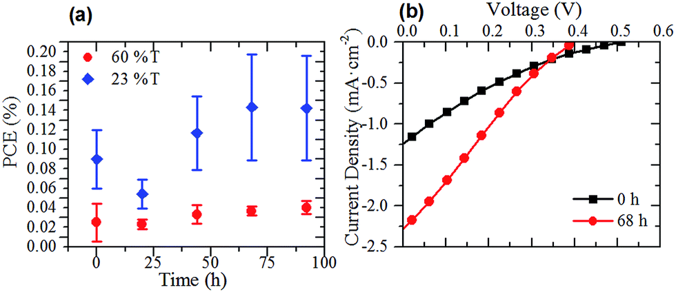 | ||
| Fig. 5 (a) PCE of G–Si cells with annealed graphene films after back and front etching and (b) representative J–V curves of a G–Si cell made with an annealed 23% T thick film immediately after back and front etching and 68 h after etching. | ||
Previous G–Si heterojunctions have shown marked improvement with doping of the graphene films. Fig. 6 shows representative J–V curves of the best performed G–Si cells both pre- and post-doping with the chemical dopants HNO3 and AuCl3. Both HNO319,48 and AuCl349 are known p-type dopants of graphene with similar charge transfer mechanisms of doping. In the case of HNO3 vapour, HNO3 molecules are adsorbed onto the surface of the graphene. Electrons are then donated from the graphene (p-doping the graphene) to the HNO3 resulting in the release of NO2 and H2O, as seen in eqn (1).19
| 4HNO3 + C+OH− + C → 2C+NO3−˙HNO3 + NO2 + 2H2O | (1) |
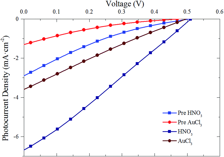 | ||
| Fig. 6 Representative J–V curves for G–Si cells pre-doping (light red and blue) and post- nitric acid (dark blue) and gold chloride (dark red) doping. | ||
Conversely AuCl3 doping involves a two-step process, seen in eqn (2) and (3).50 AuCl3 is adsorbed onto the surface and can accept electrons from the graphene (p-doping the graphene), to form AuCl2− and AuCl4. The gold in these AuCl2-complexes is then further reduced by the graphene, further p-doping it, to form gold nanoparticles.50
| 2Graphene + 2AuCl3 → 2Graphene+ + AuCl2− + AuCl4 | (2) |
| 3AuCl2− ⇌ 2Au0↓ + AuCl4− + 2Cl− | (3) |
Fig. 7 shows the PCE of pristine cells pre-doping (grey rectangles) with HNO3 (Fig. 7(a)) and AuCl3 (Fig. 7(b)) and post-doping. Exposing cells to concentrated HNO3 fumes for 2 min resulted in a large initial increase in the PCE of all of the cells with the exception of the thinnest graphene film (76% T). This large increase in PCE, shown in the representative J–V curves in Fig. 6, is mainly due to increases in the JSC of the cells. Although there are slight increases in both the FF (10–20%) and VOC (10%) of the cells when doped with HNO3 and AuCl3, they are not commensurate with the large increases often seen in the chemical doping of CVD G–Si Schottky junctions.11,18 A change in the CVD cell's VOC is often attributed to the shifting of the graphene's work function,11,19,49 which raises the Schottky barrier height of the system and hence increases the VOC. The current work however deals with films which consist of flakes of few-layer graphene stacked successively on top of each other. Work by Crowther et al.51 with graphene of varying thickness of 1–10 layers has shown that while adsorbed NO2 species can shift the Fermi level of graphene, only the two layers closest to the site of exposure are significantly doped, while no electric field is present deeper within the sample. This means that while the transport of electrons injected into the stacked graphene film should be enhanced due to the reduced sheet resistance of the upper layers,48 there is no large scale doping occurring at the G–Si interface and hence a large change in VOC is not possible.
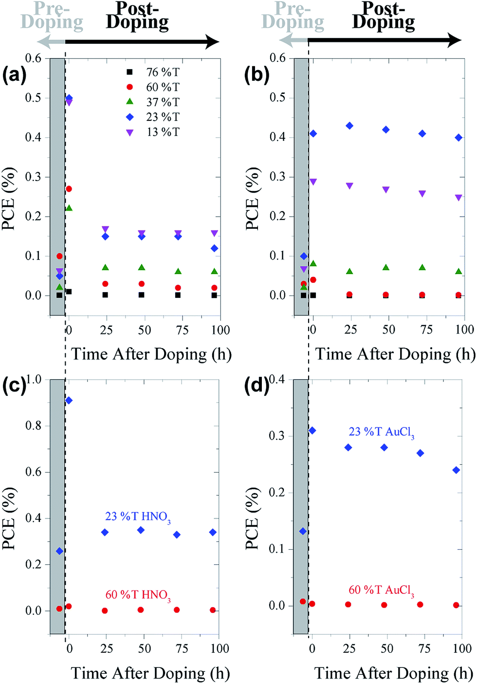 | ||
| Fig. 7 PCE of G–Si cells made with graphene films of various thicknesses both pre-doping (in grey area) and post- (a) nitric acid and (b) gold chloride doping as well as annealed film cell's PCEs both pre- and post- (c) nitric acid and (d) gold chloride doping. | ||
After this initial increase due to the rise in JSC, there is a decrease in PCE. However, for the three thicker films the PCE of the cells remains higher than the pre-doped values. In contrast to this behavior, the three thick film cells doped by spin coating of AuCl3 showed an increase in PCE which was retained over the course of testing. This difference is most likely due to the different method in which the cells are exposed to the two dopants. In the case of exposure to concentrated HNO3 vapour, HNO3 can penetrate into the graphene films as well as adsorb onto the top of the film, allowing for a supersaturation of the films. This accounts for the large increases in JSC observed when the film was tested immediately after doping. Testing the films however, along with the passage of time, allows for the excess HNO3 to evaporate, and hence the PCE of the cells drops compared to the initial test but as some HNO3 remains, the PCE still remains higher than the pre-doped instance. Doping of the cells with AuCl3 however, occurs by dynamically spin coating AuCl3 in ethyl ether solution onto the cells. In this method there is no chance for excess AuCl3 to enter the films, while the AuCl3 that is deposited forms stable nanoparticles50 and hence testing of the cells and passing of time does not result in any AuCl3 being displaced or a drop in PCE.
Fig. 7 also shows the PCE of annealed cells pre-doping (within the grey rectangles) and post-doping with HNO3 (Fig. 7(c)) and AuCl3 (Fig. 7(d)). The same trend that was present in the pristine cells is again apparent when annealed cells are doped, with both the thick and thin annealed film cells behaving in the same manner as their pristine counterparts. The overall magnitude of the lasting enhancement in both the HNO3 and AuCl3 cases is reduced in the annealed cells. In the case of the HNO3 doping, this may be explained by the lack of residual surfactant present in the graphene films. It is conceivable that one of the reasons for the enhanced performance of the pristine cells when exposed to HNO3 is that the HNO3 removes residual surfactant from the films, reducing recombination sites and enhancing the PCE, prior to any chemical doping effects. In the case of annealed cells however, this enhancement has already taken place and hence the only effect that the HNO3 can have is via chemical doping. In the case of AuCl3 doping, the lack of surfactant may however be detrimental, as metal clusters have been shown to have a good affinity for reduction promoting crown-ether-like cavities in PEO surfactants and block copolymers.52,53 Hence, when exposed to annealed surfaces with much less to no surfactant, less AuCl3 is likely to be adsorbed and less chemical doping occurs.
These doping results show promising improvements in the PCE of the cells, with the pristine AuCl3 doped 23% T cells showing an order of magnitude increase compared with the original, pristine and undoped cells. The fact that these doped cell performances remain constant over the course of 7 days in ambient cell storage conditions and that the cells in general remain stable over a period of three months (PCE ≈ 0.1% for a non-optimised cell) shows that this aqueous solution processed approach to G–Si Schottky junction presents a promising new approach.
With a maximum PCE of 0.9% and optimised stable PCE of 0.4%, the surfactant-assisted exfoliated graphene exhibits improved photovoltaic performance over reported GO and rGO cells of similar architecture (highest reported PCE of 0.3%).25 This likely stems from improved conductivity in the pristine graphene flakes. However, G–Si cells fabricated from CVD produced graphene have shown higher PCE (up to 15.6%). The improvement of the CVD derived films is a result of the larger graphene flake size reducing resistance related to flake–flake charge hopping. The higher conductivity allows for thinner films, which increases transparency allowing more light to G–Si the heterojunction and enhances the effect of doping, as discussed earlier.51
The solar cell performance should also be considered in terms of manufacturing cost and potential scalability of production. Solution processed graphene is capable of being fabricated in large scales from naturally occurring graphite with little input energy. In contrast, CVD growth is a high temperature process with limited scalability.
The initial reported PCE of CVD derived G–Si Schottky junction solar cell in 2010 was 1.65%.10 During the following 4 years gradual improvements have been achieved with the current record of 15.6% recorded early 2015.22 It is foreseeable that surfactant-assisted exfoliated graphene could follow a similar path after this initial report with incremental increases likely by optimising film doping, uniformity and increasing graphene flake size.
Furthermore, the results shown here suggest that further work in this area should focus on increasing the lateral dimensions of the graphene flakes and the conductivity of the resultant films at higher optical transparencies, as higher transparencies will result in a larger photon flux reaching the G–Si interface.
Conclusions
Surfactant-assisted exfoliated graphene was used to make transparent conducting electrodes which were then used for photovoltaic G–Si Schottky junctions. The effect of film thickness on the photovoltaic properties of these G–Si Schottky junctions was investigated and devices with an optimal film thickness of 23% T were found to have a power conversion efficiency of 0.06%. This efficiency was doubled (0.13%) when the graphene films were annealed in mild conditions. Chemical doping with nitric acid was able to increase PCE for a short duration up to 0.9% while doping with gold chloride was found to stably (>100 h) increase the power conversion efficiency to 0.4%.Author contributions
The manuscript was written through contributions of all authors. All authors have given approval to the final version of the manuscript.Acknowledgements
This work was supported by the Australian Microscopy and Microanalysis Research Facility (AMMRF). This work was also performed in part at the Flinders University node of the Australian National Fabrication Facility, a company established under the National Collaborative Research Infrastructure Strategy to provide nano- and micro-fabrication facilities for Australia's researchers. LL would also like to thank the Australian Government for an APA scholarship.Notes and references
- D. D. Tune, B. S. Flavel, R. Krupke and J. G. Shapter, Adv. Energy Mater., 2012, 2, 1043–1055 CrossRef CAS PubMed.
- Y. Ye and L. Dai, J. Mater. Chem., 2012, 22, 24224–24229 RSC.
- J. Wei, Y. Jia, Q. Shu, Z. Gu, K. Wang, D. Zhuang, G. Zhang, Z. Wang, J. Luo, A. Cao and D. Wu, Nano Lett., 2007, 7, 2317–2321 CrossRef CAS PubMed.
- Z. Li, V. P. Kunets, V. Saini, Y. Xu, E. Dervishi, G. J. Salamo, A. R. Biris and A. S. Biris, ACS Nano, 2009, 3, 1407–1414 CrossRef PubMed.
- D. D. Tune, A. J. Blanch, R. Krupke, B. S. Flavel and J. G. Shapter, Phys. Status Solidi A, 2014, 211, 1479–1487 CrossRef CAS PubMed.
- D. D. Tune, B. S. Flavel, J. S. Quinton, A. V. Ellis and J. G. Shapter, ChemSusChem, 2013, 6, 320–327 CrossRef CAS PubMed.
- D. D. Tune and J. G. Shapter, Nanomaterials, 2013, 3, 655–673 CrossRef CAS PubMed.
- Z. Li, V. P. Kunets, V. Saini, Y. Xu, E. Dervishi, G. J. Salamo, A. R. Biris and A. S. Biris, Appl. Phys. Lett., 2008, 93, 243117 CrossRef PubMed.
- Y. Jung, X. Li, N. K. Rajan, A. D. Taylor and M. A. Reed, Nano Lett., 2012, 13, 95–99 CrossRef PubMed.
- X. Li, H. Zhu, K. Wang, A. Cao, J. Wei, C. Li, Y. Jia, Z. Li, X. Li and D. Wu, Adv. Mater., 2010, 22, 2743–2748 CrossRef CAS PubMed.
- G. Fan, H. Zhu, K. Wang, J. Wei, X. Li, Q. Shu, N. Guo and D. Wu, ACS Appl. Mater. Interfaces, 2011, 3, 721–725 CAS.
- Y. Wu, X. Zhang, J. Jie, C. Xie, X. Zhang, B. Sun, Y. Wang and P. Gao, J. Phys. Chem. C, 2013, 117, 11968–11976 CAS.
- T. Feng, D. Xie, Y. Lin, Y. Zang, T. Ren, R. Song, H. Zhao, H. Tian, X. Li, H. Zhu and L. Liu, Appl. Phys. Lett., 2011, 99, 233505 CrossRef PubMed.
- K. Ihm, J. T. Lim, K.-J. Lee, J. W. Kwon, T.-H. Kang, S. Chung, S. Bae, J. H. Kim, B. H. Hong and G. Y. Yeom, Appl. Phys. Lett., 2010, 97, 032113 CrossRef PubMed.
- J. B. Bult, R. Crisp, C. L. Perkins and J. L. Blackburn, ACS Nano, 2013, 7, 7251–7261 CrossRef CAS PubMed.
- X. Li, D. Xie, H. Park, T. H. Zeng, K. Wang, J. Wei, M. Zhong, D. Wu, J. Kong and H. Zhu, Adv. Energy Mater., 2013, 3, 1029–1034 CrossRef CAS PubMed.
- W. Jie and J. Hao, Nanoscale, 2014, 6, 6346–6362 RSC.
- T. Feng, D. Xie, Y. Lin, H. Zhao, Y. Chen, H. Tian, T. Ren, X. Li, Z. Li, K. Wang, D. Wu and H. Zhu, Nanoscale, 2012, 4, 2130–2133 RSC.
- X. Li, D. Xie, H. Park, M. Zhu, T. H. Zeng, K. Wang, J. Wei, D. Wu, J. Kong and H. Zhu, Nanoscale, 2013, 5, 1945–1948 RSC.
- X. Miao, S. Tongay, M. K. Petterson, K. Berke, A. G. Rinzler, B. R. Appleton and A. F. Hebard, Nano Lett., 2012, 12, 2745–2750 CrossRef CAS PubMed.
- E. Shi, H. Li, L. Yang, L. Zhang, Z. Li, P. Li, Y. Shang, S. Wu, X. Li, J. Wei, K. Wang, H. Zhu, D. Wu, Y. Fang and A. Cao, Nano Lett., 2013, 13, 1776–1781 CAS.
- Y. Song, X. Li, C. Mackin, X. Zhang, W. Fang, T. Palacios, H. Zhu and J. Kong, Nano Lett., 2015, 15, 2104–2110 CrossRef CAS PubMed.
- W. S. Hummers and R. E. Offeman, J. Am. Chem. Soc., 1958, 80, 1339 CrossRef CAS.
- D. Li, M. B. Muller, S. Gilje, R. B. Kaner and G. G. Wallace, Nat. Nanotechnol., 2008, 3, 101–105 CrossRef CAS PubMed.
- M. Zhu, X. Li, Y. Guo, X. Li, P. Sun, X. Zang, K. Wang, M. Zhong, D. Wu and H. Zhu, Nanoscale, 2014, 6, 4909–4914 RSC.
- D. T. Phan, R. K. Gupta, G. S. Chung, A. A. Al-Ghamdi, O. A. Al-Hartomy, F. El-Tantawy and F. Yakuphanoglu, Sol. Energy, 2012, 86, 2961–2966 CrossRef CAS PubMed.
- G. Kalita, K. Wakita, M. Umeno and M. Tanemura, Phys. Status Solidi RRL, 2013, 7, 340–343 CrossRef CAS PubMed.
- S. K. Behura, S. Nayak, I. Mukhopadhyay and O. Jani, Carbon, 2014, 67, 766–774 CrossRef CAS PubMed.
- P. Blake, P. D. Brimicombe, R. R. Nair, T. J. Booth, D. Jiang, F. Schedin, L. A. Ponomarenko, S. V. Morozov, H. F. Gleeson, E. W. Hill, A. K. Geim and K. S. Novoselov, Nano Lett., 2008, 8, 1704–1708 CrossRef PubMed.
- Y. Hernandez, V. Nicolosi, M. Lotya, F. M. Blighe, Z. Sun, S. De, I. T. McGovern, B. Holland, M. Byrne, Y. K. Gun'Ko, J. J. Boland, P. Niraj, G. Duesberg, S. Krishnamurthy, R. Goodhue, J. Hutchison, V. Scardaci, A. C. Ferrari and J. N. Coleman, Nat. Nanotechnol., 2008, 3, 563–568 CrossRef CAS PubMed.
- K. S. Novoselov, A. K. Geim, S. V. Morozov, D. Jiang, Y. Zhang, S. V. Dubonos, I. V. Grigorieva and A. A. Firsov, Science, 2004, 306, 666–669 CrossRef CAS PubMed.
- K. S. Novoselov, D. Jiang, F. Schedin, T. J. Booth, V. V. Khotkevich, S. V. Morozov and A. K. Geim, Proc. Natl. Acad. Sci. U. S. A., 2005, 102, 10451–10453 CrossRef CAS PubMed.
- A. O'Neill, U. Khan, P. N. Nirmalraj, J. Boland and J. N. Coleman, J. Phys. Chem. C, 2011, 115, 5422–5428 Search PubMed.
- A. B. Bourlinos, V. Georgakilas, R. Zboril, T. A. Steriotis and A. K. Stubos, Small, 2009, 5, 1841–1845 CrossRef CAS PubMed.
- Y. Hernandez, M. Lotya, D. Rickard, S. D. Bergin and J. N. Coleman, Langmuir, 2009, 26, 3208–3213 CrossRef PubMed.
- U. Khan, A. O'Neill, M. Lotya, S. De and J. N. Coleman, Small, 2010, 6, 864–871 CrossRef CAS PubMed.
- U. Khan, H. Porwal, A. O'Neill, K. Nawaz, P. May and J. N. Coleman, Langmuir, 2011, 27, 9077–9082 CrossRef CAS PubMed.
- M. Lotya, Y. Hernandez, P. J. King, R. J. Smith, V. Nicolosi, L. S. Karlsson, F. M. Blighe, S. De, Z. Wang, I. T. McGovern, G. S. Duesberg and J. N. Coleman, J. Am. Chem. Soc., 2009, 131, 3611–3620 CrossRef CAS PubMed.
- A. A. Green and M. C. Hersam, Nano Lett., 2009, 9, 4031–4036 CrossRef CAS PubMed.
- T. Hasan, F. Torrisi, Z. Sun, D. Popa, V. Nicolosi, G. Privitera, F. Bonaccorso and A. C. Ferrari, Phys. Status Solidi B, 2010, 247, 2953–2957 CrossRef CAS PubMed.
- L. Guardia, M. J. Fernández-Merino, J. I. Paredes, P. Solís-Fernández, S. Villar-Rodil, A. Martínez-Alonso and J. M. D. Tascón, Carbon, 2011, 49, 1653–1662 CrossRef CAS PubMed.
- D. J. Finn, M. Lotya, G. Cunningham, R. J. Smith, D. McCloskey, J. F. Donegan and J. N. Coleman, J. Mater. Chem. C, 2014, 2, 925–932 RSC.
- F. Withers, H. Yang, L. Britnell, A. P. Rooney, E. Lewis, A. Felten, C. R. Woods, V. Sanchez Romaguera, T. Georgiou, A. Eckmann, Y. J. Kim, S. G. Yeates, S. J. Haigh, A. K. Geim, K. S. Novoselov and C. Casiraghi, Nano Lett., 2014, 14, 3987–3992 CrossRef CAS PubMed.
- A. C. Ferrari, J. C. Meyer, V. Scardaci, C. Casiraghi, M. Lazzeri, F. Mauri, S. Piscanec, D. Jiang, K. S. Novoselov, S. Roth and A. K. Geim, Phys. Rev. Lett., 2006, 97, 187401 CrossRef CAS.
- S. Bae, H. Kim, Y. Lee, X. Xu, J.-S. Park, Y. Zheng, J. Balakrishnan, T. Lei, H. Ri Kim, Y. I. Song, Y.-J. Kim, K. S. Kim, B. Ozyilmaz, J.-H. Ahn, B. H. Hong and S. Iijima, Nat. Nanotechnol., 2010, 5, 574–578 CrossRef CAS PubMed.
- S. De, P. J. King, M. Lotya, A. O'Neill, E. M. Doherty, Y. Hernandez, G. S. Duesberg and J. N. Coleman, Small, 2010, 6, 458–464 CrossRef CAS PubMed.
- V. Berry, Carbon, 2013, 62, 1–10 CrossRef CAS PubMed.
- A. Kasry, M. A. Kuroda, G. J. Martyna, G. S. Tulevski and A. A. Bol, ACS Nano, 2010, 4, 3839–3844 CrossRef CAS PubMed.
- Y. Shi, K. K. Kim, A. Reina, M. Hofmann, L.-J. Li and J. Kong, ACS Nano, 2010, 4, 2689–2694 CrossRef CAS PubMed.
- K. K. Kim, A. Reina, Y. Shi, H. Park, L.-J. Li, Y. H. Lee and J. Kong, Nanotechnology, 2010, 21, 285205 CrossRef PubMed.
- A. C. Crowther, A. Ghassaei, N. Jung and L. E. Brus, ACS Nano, 2012, 6, 1865–1875 CrossRef CAS PubMed.
- T. Sakai and P. Alexandridis, J. Phys. Chem. B, 2005, 109, 7766–7777 CrossRef CAS PubMed.
- P. Alexandridis, Chem. Eng. Technol., 2011, 34, 15–28 CrossRef CAS PubMed.
| This journal is © The Royal Society of Chemistry 2015 |