
Effect of various encapsulants for frameless glass to glass Cu(In,Ga)(Se,S)2 photovoltaic module
JungYup Yanga,
Dongho Leea,
DoHyun Baeka,
DongSeop Kima,
Junggyu Nam*a and
PilHo Huh*b
aPhotovoltaic Development Team, Samsung SDI Co., Ltd., CheonanSi, 331-300, Korea. E-mail: zignamu@gmail.com
bDepartment of Polymer Science and Engineering, Pusan National University, Busan 609-735, Korea. E-mail: pilho.huh@pusan.ac.kr
First published on 29th May 2015
Abstract
Cu(In,Ga)(Se,S)2 (CIGSS) modules with a frameless glass to glass (G2G) structure were successfully fabricated by replacing the currently used ethylene vinyl acetate (EVA) with new encapsulants such as polyolefins (POE), ionomer (IO) and liquid silicon (LSI), and their characteristics including optical, mechanical, and reliability properties were investigated. Most of the solid films for encapsulation except POE exhibit similar light transmittance in the visible-infrared wavelength range, while LSI shows the highest light transmittance with a difference of more than 2% in the overall wavelength range. The G2G structure encapsulated with IO exhibits superior values for the adhesion strength at which interface failure occurs (about 7.5 MPa) compared to other encapsulants. Water vapor transmittance ratio (WVTR) values of the encapsulants were evaluated to determine their suitability as water-resistant materials in terms of the CIGSS G2G structure. The IO encapsulant had the lowest WVTR value of about 1.75 g per m2 per day. Changes of cell-to-module (CTM) conversion ratio in the CIGSS G2G structure using various encapsulants were investigated using I–V measurements. The CIGSS G2G structure encapsulated by LSI shows the best CTM conversion ratio, since the module process occurs at the lowest temperature as compared with other encapsulants, therefore the module has a smaller thermal transient effect. Finally, the long-term reliability of the CIGSS modules based on various encapsulants was also evaluated by damp heat testing.
Polyvinyl butyral (PVB) was generally utilized for thin film photovoltaic (PV) modules in the 1970s. Unfortunately, these modules exhibited power loss and failure due to the light transmittance loss from encapsulant yellowing when water or moisture was introduced through the module edge.1,2 Therefore, ethylene vinyl acetate (EVA) has since substituted PVB as a basic encapsulant for thin film modules in many photovoltaic applications. However, the overall properties of the currently used EVA have also been reported to be gradually reduced after the reliability test (especially IEC 61646 for thin film modules and IEC 61215 for crystalline modules) and field test.3–5 In addition, the rework procedure for PV modules incorporating EVA is more difficult than that for modules with thermoplastic encapsulants because of the cross-linking properties of EVA. Therefore, EVA is unfavorable for reusable modules, especially CdTe and Cu(In,Ga)(Se,S)2 (CIGSS) based modules which include rare metals.
Thin film polycrystalline CIGSS solar cells have attracted interest in recent years due to their high efficiencies of over 20%.6 Also, CIGSS solar modules have been commercialized during the last decade, with accelerating growth in recent years. However, there is a paucity of study with respect to power losses that result from module fabrication processes, especially power loss by the thermal transient effect (TTE),7 which can be defined as the behavior of power reduction resulting from a lamination process. The TTE is caused by elevated temperatures, lamination time, and applied pressure. In particular, the thermal budget of the intermediate material in a PV module could be a key characteristic to generate a high power output in the cell-to-module (CTM) conversion ratio because of a low TTE. Also, in the fabrication of a CIGSS module with a frameless glass to glass (G2G) structure, there is much greater emphasis on the water resistance of the encapsulant used due to the moisture sensitivity of the CIGSS cell.8,9 Therefore, the selection of an effective encapsulant could also be an important factor to support the stability of a PV module for long-term operation.
In this paper, thin film CIGSS modules have been fabricated based on various encapsulants such as EVA, polyolefins (POE), ionomer (IO) and liquid silicon (LSI) under similar lamination conditions. Encapsulants other than EVA sheets have recently been introduced and applied in the packaging process of photovoltaic modules in the research field.10–12 Utilization of IO and POE, which are typically thermoplastics, has been widely adopted to replace EVA in the research field. These hydrocarbon-based materials require stabilizers to guarantee long operational lifetime and enhance the stability of PV module performance. Poly(dimethyl siloxane) (PDMS)-based silicone encapsulant is a typical thermo-setting material with inherent ultraviolet (UV) and thermal stability. It is reported from industrial research that PV modules using silicone as an encapsulant exhibit no significant damage in low temperature tests and show relatively high PV module performance in colder regions. In contrast to previous reports, our research focused on finding an encapsulant for thin film CIGSS modules that could be used to apply a frameless G2G structure without edge sealing materials. In addition, we have studied the long-term reliability of CIGSS modules with different encapsulants as well as power loss during the module process. Properties such as adhesion on glass, refractive index matching for light transmittance, and TTE for power loss were evaluated in order to apply the frameless G2G structure. In order to achieve the qualified tests, the estimation of moisture resistivity in the intermediate materials was undertaken with regards to the individual raw film and the power loss of CIGSS modules with a frameless G2G structure after damp heat reliability testing.
Scheme 1 shows a typical process flow to produce a CIGSS thin film module. The fabrication of the CIGSS module was carried out via two processes, denoted frontend and backend, as shown in Scheme 1. In the first step of the frontend process, the Mo back electrode was deposited at 300 nm thickness by a DC magnetron sputtering system on cleaned high strain point glass at room temperature. The metallic precursors of Cu:Ga/In were sequentially deposited by DC sputtering on the Mo back electrode. In the second step, the completed CIGSS structure was formed by selenization and sulfurization through chemical reaction with H2Se and H2S gases, respectively. A heterojunction was formed by deposition of a Zn(O,OH,S) buffer layer of about 5 nm by a chemical bath deposition (CBD) process in order to reduce shunt path and improve interface quality. The Zn-based buffer layer was selected for its eco-friendliness and good absorption at short wavelengths. A transparent conducting oxide (TCO) layer was deposited on the CBD buffer layer using low pressure chemical vapor deposition. One laser and two mechanical scribing techniques for monolithically integrated modules were applied to create the three patterns P1–P3. The frontend process is described in more detail elsewhere.13
 | ||
| Scheme 1 Typical process flow for fabrication of a CIGSS based thin film module, consisting of frontend and backend processes. | ||
For the wire interconnection, the TCO/buffer/CIGSS layers around the glass edge were removed by mechanical scriber to expose the Mo back contact. To protect the CIGSS module from moisture and enhance long term stability, the layers at the edge of the module were removed by laser, isolating a 12 mm perimeter from the glass edge. The tape-like conducting wire was attached to the exposed Mo layer and then laminated. The lamination assemblies were prepared with a front cover glass/encapsulant/CIGSS monolithic cells structure (the monolithic cells being defined as the series of connected CIGSS cells before encapsulation) for the analysis of device properties based on various encapsulants. The front cover glass used in our experiment was a 3.2 mm thick non-antireflection coated soda-lime tempered glass. The lamination process was carried out at about 140 °C for solid encapsulants and at about 100 °C for liquid silicon (LSI) under a pressure of 100 kPa. Sequential process (pre-heat, lamination, and cooling steps) were performed over the course of about 30 minutes.
The glass (1.8 mm thick)/encapsulant/glass (1.8 mm thick) and glass (1.8 mm thick)/encapsulant/CIGSS samples were cut into small 2.5 × 2.5 cm2 pieces with a diamond saw for measurements of transmittance spectra and adhesion strength. The CIGSS modules were formed at a size of 30 × 30 cm2 for device performance and reliability testing. The light transmittance was measured through the direct detection of transmitted light that appeared as reflectance, absorption, and light scattering in the laminated structure. The adhesion strength of the various encapsulants was investigated by compressive shear strength (CSS) testing using a glass/encapsulant/CIGSS laminated structure. The CSS test samples were comprised of the laminated encapsulant between two glasses (the CIGSS cell substrate is also a glass) to estimate the combined compression and shear. The interface of the glass/encapsulant breaks once a critical value of shear stress is reached. The critical value of stress is taken as a measure of adhesion. The samples were loaded with compressive and shearing components at 45° to the loading direction. The I–V curves were measured under AM 1.5, 100 mW cm−2 illumination at 25 °C before and after lamination. The water vapor transmission ratio (WVTR) of encapsulants was measured using a MOCON Permatran (ASTM-F1249).
Fig. 1 shows the optical transmittance of intermediate materials in the glass/encapsulant/glass structure measured by UV-visible spectroscopy. As shown in Fig. 1, LSI has a much higher transmittance value, which is about 2% above those of the other encapsulants in the visible wavelength range. The significant difference could be explained as the effect of a comparable refractive index between LSI and glass. In addition, the LSI encapsulant was significantly more transparent than the solid encapsulants over the range of 350 nm to 400 nm than the solid encapsulants, because solid encapsulant sheets can be mixed with an anti-UV component by manufacturers, which results in a decrease in the transmittance value at short wavelengths. This 2% light difference could be responsible for the immediately increased electrical output current in the CIGSS module. In the case of the POE encapsulant, the transmittance spectrum shows the lowest value at about 400–750 nm due to the haze effect. The haze effect of an encapsulant material shows how much visible light is diffused or scattered and causes a loss of module power due to a milky appearance. The order of transmittance values is LSI > EVA > ionomer (IO) > POE.
 | ||
| Fig. 1 UV-visible transmittance spectra of various encapsulation materials. | ||
De-lamination caused by environmental stress such as temperature, humidity, and mechanical load is one of the most critical failure modes of thin film CIGSS modules with a frameless G2G structure for long-term reliability. De-lamination resistivity based on various intermediate materials was indirectly evaluated through adhesion strength testing on the glass/encapsulant/CIGSS laminate structure. Strong adhesion is essentially required to avoid de-lamination. Glass/encapsulant/CIGSS laminates were loaded with compressive and shearing components at 45° to the loading direction. If an interface in a laminate is out of joint, the load would drop. The critical load is converted into shear stress expressed in MPa as a function of the laminate area.14 The adhesion strengths of various encapsulants are displayed in Fig. 2. The glass/IO/CIGSS laminate exhibits a superior value for the shear stress average at which interface failure occurs of 7.48 MPa, in comparison with the values for laminates encapsulated with EVA (average 2.5 MPa), POE (average 0.834 MPa) and LSI (average 0.092 MPa). In addition, the glass/IO/CIGSS laminate undergoes complete separation of the CIGSS top layer when interface failure occurs. This result indicates that the interface itself is not degraded gradually but broken once a critical shear stress (∼7.48 MPa) is reached. It may also be considered that adhesion between IO and CIGSS is equivalent to the entire surface of a CIGSS module. On the other hand, in the case of intermediate materials other than IO the glass/encapsulant interface is partially torn with increasing stress levels. All encapsulants except LSI can be used as an adhesion layer between glass and the CIGSS cell of the CIGSS module. The LSI encapsulant needs to have its adhesion improved, or a new module structure needs to be designed, in order for LSI to be applied in a CIGSS module.
 | ||
| Fig. 2 Adhesion strengths measured by universal peel testing machine for glass/encapsulant/CIGSS monolithic cells laminates using LSI, EVA, IO, or POE as an interlayer. | ||
Power loss of CIGSS modules after the lamination process is calculated using the CTM conversion ratio, which is defined by the following equation:15

CTM is the ratio of the module output power to the initial monolithic cell power in the form of sunlight. The CTM conversion ratio is strongly dependent upon the power loss that occurs in the fabrication of the PV module and may be affected by the following factors: series resistance by electrical interconnection, light absorption by front glass and encapsulant, and TTE from the lamination process. A higher CTM conversion ratio will lead to the improvement of output power for the produced CIGSS module. The CTM conversion ratio of individual glass/encapsulant/CIGSS modules with a size of 30.0 × 30.0 cm2 using various encapsulant materials was estimated under standard test conditions at one Sun (1000 W m−2). Fig. 3 illustrates the typical current–voltage curves of the monolithic cells and CIGSS modules, and their electrical characteristics are summarized in Table 1. Comparing the CTM ratios, the power losses of the CIGSS modules other than the one using LSI were caused by a sharp decrease in fill factor (FF) due to the increasing series resistance as shown in Fig. 3(a)–(c), whereas the CIGSS module with LSI encapsulant showed only a slight decrease in FF (Fig. 3(d)). In addition, we found a roll-over I–V characteristic in the modules using solid encapsulants (Fig. 3(a)–(c)). As mentioned above, it is well known that the power loss from decreasing FF may be due to the increase in series resistance, decrease in shunt resistance by distortion of the buffer/CIGSS interface, and TTE. In the CIGSS module with solid encapsulants, we always observed an irreversible 1-Sun I–V curve even if light soaking was performed at two hours as well a large drop in FF, which is not caused by series resistance of the wire and wire/Mo contact. Therefore, instead of a well-known TTE (such as meta-stability), the phenomenon in the CIGSS modules with solid encapsulants may be considered as a different kind of TTE resulting from the adhesion problems of thin film stress and thermal effects during the lamination process. On the other hand, it may also be considered that the relatively high CTM conversion ratio for the module laminated with LSI has a small effect on the TTE due to the low lamination temperature (∼100 °C), weak thin film stress from low adhesion, and relatively little distortion of the buffer/CIGSS interface as a result of the weak thin film stress. The individual CTM conversion ratios of glass/solid encapsulant/CIGSS modules are relatively low (81–85.2%), as shown in Table 1. In comparison to the initial monolithic output power, the output power of the CIGSS module with LSI encapsulant is only slightly decreased. The CTM conversion ratio of the glass/POE/CIGSS module is relatively the lowest (80.92%) and may be explained by the change in short circuit current, which corresponds well to the transmittance data in Fig. 2.
 | ||
| Fig. 3 I–V curves of glass/encapsulant/CIGSS modules made with solid encapsulants EVA (a), IO (b), and POE (c) or liquid encapsulant LSI (d) with a size of 30.0 × 30.0 cm2, and their initial CIGSS monolithic cells. All samples were measured after two hours of light soaking. | ||
| Encapsulant type | Isc (A) | Voc (V) | FF (%) | Eff. (%) | Pmax (W) | CTM (%) | |
|---|---|---|---|---|---|---|---|
| EVA | Monolithic cell | 0.532 | 36.61 | 66.85 | 14.47 | 13.02 | 84.5 |
| Module | 0.525 | 37.16 | 56.38 | 12.23 | 11.00 | ||
| POE | Monolithic cell | 0.538 | 37.55 | 67.97 | 15.26 | 13.73 | 81.0 |
| Module | 0.520 | 36.94 | 57.87 | 12.34 | 11.12 | ||
| Ionomer | Monolithic cell | 0.534 | 37.08 | 67.38 | 14.81 | 13.34 | 85.2 |
| Module | 0.519 | 36.49 | 59.97 | 12.63 | 11.36 | ||
| LSI | Monolithic cell | 0.530 | 38.10 | 67.21 | 15.09 | 13.57 | 96.1 |
| Module | 0.532 | 37.54 | 65.23 | 14.49 | 13.04 | ||
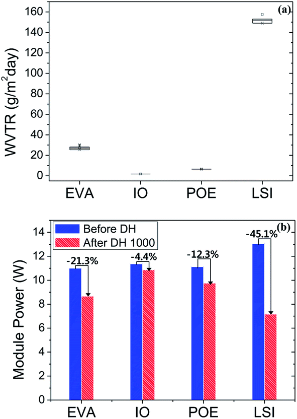
Moisture may be fatal to CIGSS modules because a generated acid would damage the CIGSS absorber. This moisture ingress could affect the CIGSS cell efficiency and lifetime because of the accelerated degradation of the CIGSS cell. Fig. 4(a) shows the WVTR values of various encapsulants, which may be used to determine the effect of moisture ingress in CIGSS modules and to select an effective encapsulant for these devices. The IO encapsulant presents the lowest WVTR value of about 1.75 g per m2 per day, while the LSI encapsulant sheet shows the highest WVTR value of above 150 g per m2 per day, as evidenced from Fig. 4(a). Silicone materials are generally known to have relatively high moisture permeation rates.16 The long-term stability of solar cells is typically studied by damp heat (DH) testing because it is one of the major failures in IEC qualification testing of thin film PV modules. PV modules must degrade within 10% in relative output power comparing with initial power to pass DH test (module power measurement after storage for 1000 hours at 85 degree and 85% relative humidity). Fig. 4(b) shows the changes in the CIGSS module power before and after the DH test. All CIGSS modules except the one using IO fail with more than 10% loss in efficiency at 85 °C and 85% RH over 1000 hours, whereas there is little change in the glass/IO/CIGSS module I–V characteristics. After DH exposure, the powers of glass/EVA/CIGSS and glass/LSI/CIGSS structures were decreased by 21.3% and 45.1%, respectively. Only the glass/IO/CIGSS module retains 95.6% of its original output power after the DH test. This result indicates that almost all the encapsulation materials could not provide sufficiently low moisture permeability on their own to stop edge ingress in the frameless G2G CIGSS module without edge sealing material. To protect the frameless G2G CIGSS module without edge sealing material from the moisture, the encapsulant needs to have a low WVTR value and strong adhesion property, even though the lamination was performed at a lower temperature process. Otherwise, a change of module design would become an essential prerequisite to the use of various encapsulants, such as a CIGSS module with edge sealing material or a frame-type CIGSS module.
 | ||
| Fig. 4 (a) Barrier measurements of encapsulant sheets at 38 °C, 100% RH to determine WVTR values and (b) module power changes for 30.0 × 30.0 cm2 CIGSS modules with different encapsulants after the DH test. | ||
In conclusion, we have investigated the light transmittance, adhesion to glass, CTM conversion ratio, and reliability properties of CIGSS laminates based on the currently used EVA and newly introduced POE, IO, and LSI. Although IO shows good long-term reliability with an improvement of more than 200% in adhesion and a low WVTR value compared to the other encapsulants, relatively high power loss may result from the TTE caused by excess adhesion strength and lamination temperature. In spite of the long-term reliability problem resulting from the relatively low adhesion and WVTR properties of LSI, it provides only a slight decrease in power because of the enhanced transmittance and less effect on the TTE. Although the four encapsulants are not immediately satisfactory for application to the frameless G2G CIGSS module without edge sealing material, the optimized properties of an encapsulant for fabricating a frameless G2G thin film CIGSS module with high CTM conversion ratio and good reliability are estimated in this work. Firstly, the encapsulants need to have low WVTR and strong adhesion property even if lamination process was performed under a lower thermal condition. Low WVTR and strong adhesion are closely connected with the reliability properties of the module. Secondly, TTE behavior is a much more important factor for thin film CIGSS modules because the efficiency of the CIGSS cell can be degraded by thermal and mechanical stress during the lamination process. Finally, to be applied in a thin film CIGSS module with a frameless G2G structure, an encapsulant needs to achieve a trade-off between damp heat stability and TTE. For example, high adhesion strength is advantageous for reliability and disadvantageous for thin film stress by TTE during the lamination process. Therefore, it is considered that an accurate understanding of encapsulant properties and this trade-off relation could provide an efficient way to achieve high CTM conversion ratios and good reliability for thin film CIGSS modules with a frameless G2G structure without edge sealing materials.
Acknowledgements
This work was supported by Korea Institute of Energy Technology Evaluation and Planning (KETEP) (grant no. 20119010100010) Research Grant in 2011 and Pusan National University Research Grant in 2014.References
- J. Pern, Module encapsulation materials, processing and testing, APP International PV Reliability Workshop, China, 2008 Search PubMed.
- R. Dub, S. Chattopadhyay, V. Kuthanazhi, J. Joseph John, B. M. Arora, A. Kottantharayil, K. L. Narasimhan, C. S. Solanki, V. Kuber and J. Vasi, All-India survey of photovoltaic module degradation: 2013, http://www.ncpre.iitb.ac.in/uploads/All_India_Survey_of_Photovoltaic_Module_Degradation_2013.pdf.
- A. W. Czanderna and F. J. Pern, Sol. Energy Mater. Sol. Cells, 1996, 43, 101 CrossRef CAS.
- R. T. Tucker, Primers and Adhesion, Proc. of First Thin-Film Module Reliability National Team Meeting at NREL, Golden, Co, 2002 Search PubMed.
- G. Jorgensen, K. Terwilliger, G. Barber, S. Glick and T. McMahon, Adhesion after damp heat, Proc. of First Thin-Film Module Reliability National Team Meeting at NREL, Golden, Co, 2002 Search PubMed.
- M. A. Green, K. Emery, Y. Hishikawa, W. Warta and E. D. Dunlop, Prog. Photovoltaics, 2014, 22, 701 Search PubMed.
- D. E. Tarrant and R. R. Gay, NREL final technical report, 2006, NREL/SR-520-38805 Search PubMed.
- J. Wennerberg, J. Kessler and L. Stolt, Sol. Energy Mater. Sol. Cells, 2003, 75, 47 CrossRef CAS.
- M. D. Kempe, Sol. Energy Mater. Sol. Cells, 2006, 90, 2720 CrossRef CAS PubMed.
- M. A. Green, Silicon photovoltaic modules: A brief history of the first 50 years, Prog. Photovoltaics, 2005, 13, 447 Search PubMed.
- P.-O. Westin, P. Neretnieks and M. Edoff, 25th European Photovoltaic Solar Energy Conference, 2006, p. 2470 Search PubMed.
- D. Miller, M. D. Kempe, S. H. Glick and S. R. Kurtz, Proc. 35th IEEE PVSC, 2010, p. 000262 Search PubMed.
- J. Y. Yang, D. Lee, K. S. Huh, S. J. Jung, J. W. Lee, H. C. Lee, D. Baek, B. J. Kim, D. Kim, J. Nam, G. Y. Kim and W. Jo, RSC Adv., 2015, 5, 40719 RSC.
- A. Jagota, S. J. Bennison and C. A. Smith, Int. J. Fract., 2000, 104, 105 CrossRef CAS.
- J. Y. Yang, Y. K. Ahn, P. H. Huh, J. G. Nam, M. Park, M. G. Kim, J. Y. Lee, Y. G. Ji and D. S. Kim, J. Renewable Sustainable Energy, 2013, 5, 052003 CrossRef PubMed.
- Polymeric Materials Encyclopedia, ed. J. C. Salamone, CRC Press, 1996, vol. 4 Search PubMed.
| This journal is © The Royal Society of Chemistry 2015 |