
Fabrication of multi-layered DNA nanostructures using single-strand and double-crossover tile connectors†
Anshula Tandon‡
,
Sekhar Babu Mitta‡,
Srivithya Vellampatti‡,
Byeonghoon Kim‡,
Junwye Lee,
Soyeon Kim,
Junyoung Son and
Sung Ha Park*
Department of Physics and Sungkyunkwan Advanced Institute of Nanotechnology (SAINT), Sungkyunkwan University, Suwon 440-746, Korea. E-mail: sunghapark@skku.edu
First published on 4th May 2015
Abstract
DNA is an excellent and extraordinarily versatile building block that can be used to construct nanoscale objects and arrays of increasing complexity, and as a result, a considerable amount of progress has been made in DNA-directed molecular self-assembly. Here, we demonstrate the sequential fabrication of three-dimensional multi-layered DNA nanostructures by utilizing single-strand and double-crossover tile (DX) designs via substrate-assisted growth and multi-step annealing methods. We used both layering and connector tiles to synthesize the base layer for both the single strand-based and DX tile-based designs. Layering without and with connector tiles was used to produce double-layer and multi-layer designs for single strand-based designs, but only layering tiles were used for the DX tile-based design. Connector tiles provided appropriate sticky-end sets to form the designed lattice structures. Atomic force microscopy revealed that the spacing between the tiles was in good agreement with the design scheme, but the heights of the multi-layered nanostructures were found to be slightly lower than expected due to suppression by the substrate. This kind of step-wise multi-layer assembly may produce a variety of spacings to incorporate different guest molecules or aid the attachment of various types of biomolecules and nanomaterials in parallel arrays along the layers.
In recent years, there has been a tremendous amount of interest to develop different concepts and approaches to realize self-assembled systems. In this regard, DNA is a promising construction material for use in nanotechnology. The highly specific Watson–Crick hydrogen bonding allows for programmability with artificial DNA receptor moieties while also providing mechanical rigidity and physicochemical stability. Seeman et al. pioneered molecular recognition properties that are useful for the design of complex mesoscopic structures exclusively with DNA.1 The rapid growth in the field of DNA nanotechnology has produced tools to use DNA to engineer various multi-dimensional nanostructures of essentially arbitrary shapes.2–13 Over the past few years, three-dimensional (3D) DNA nanostructures have been the object of intense study, and various strategies have been implemented to construct nanotubes, discrete and extended 3D structures.7–21 However, long-range periodic order has not yet been achieved with DNA-based self-assembly as a result of structural instability and a lack of specific assembly in 3D design, especially with tile-based design schemes. The self-assembly of DNA-based nanostructures offers huge potential for diagnostics, biosensors, and physical devices.22–27
In this paper, we report on the tile-based design and fabrication of 3D nanostructures via self-assembly of DNA double-crossovers (DX) with dimensions of 12.2 nm (length, 37 nucleotides × 0.34) × 4 nm (width, diameter of two duplex). DX has been extensively investigated due to its structural rigidity, high yield, and compact design using B-form DNA.28 A DX tile is formed by hybridizing two parallel duplexes through two DX junctions cross-linking DNA backbones between two duplexes. These tiles have sticky ends at each of their four termini that preferentially match the sticky-ends of the consequent DNA tiles, facilitating further assembly into tiling lattices. Our main goal was to fabricate different multi-layered 3D DNA nanostructures via single strand-based and DX tile-based design schemes via substrate-assisted growth (SAG) and multi-step annealing. We used layering and connector tiles to synthesize the base layer for both design schemes. For the single strand-based design, layering tiles without and with connector tiles were used to construct double-layered and multi-layered structures, but for the DX tile-based design, only layering tiles were used. The connector tiles were programmed with the appropriate sticky-end sets to form the designed lattice structures.
Our experimental strategy involved sequentially fabricating vertically-grown multi-layered structures starting from the formation of a single- (base), double- and finally multi-layered structure. The fabrication scheme for the multilayer nanostructure formed via single strand-based design is depicted in the 3D illustration shown in Fig. 1-(a). For the overall process of the layer-by-layer assembly via single strand-based design, we used two distinct tile types that are known to act as layering and connector tiles. Layering tiles are formed by modifying a DX tile to generate an extra sticky-end that protrudes up and down normal to the surface of the DX tile. These are referred to as a pillar strands and are shown as white pillars in the 3D illustration in Fig. 1-(a). This pillar strand consists of 32 base pairs with 15 repetitions of either GT or AC bases to link the layers and two Ts for a spacer. The pillar is considered to be the significant part of this design since it will aid in attaching consecutive layers to each other.
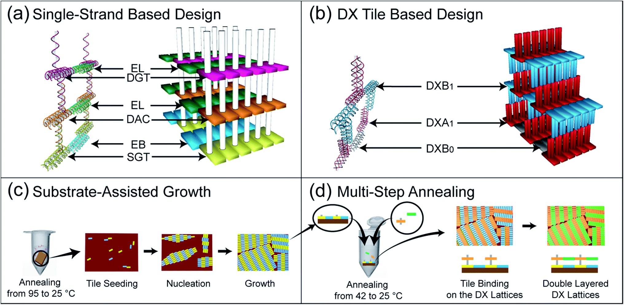 | ||
| Fig. 1 Schematic of the experimental strategy adopted to fabricate multi-layered DNA nanostructures via single strand-based and DX tile-based designs. (a) DNA nanostructure design of the layer-by-layer assembly for multi-layer formation via single strand-based design. Here, SGT, DAC, DGT, EB, and EL represent a single-side strand with 15 GT repeats, double-side strands with 15 AC repeats, double-side strands with 15 GT repeats, extension base, and extension layer tiles, respectively. (b) DNA nanostructure design of the layer-by-layer assembly of multi-layer formation via DX tile-based design. DXA1, DXB0, and DXB1 represent double-crossover A1, double-crossover B0 and double-crossover B1 tiles, respectively. (c) Schematic diagram showing structure fabrication via substrate-assisted growth. (d) Schematic diagram showing structure fabrication by the multi-step annealing method. | ||
The sequence of the pillar strand for one DX tile is complementary to that of the adjoining DX tile. The centre-to-centre distance between the pillar strands is calculated as the size of two DX tiles, which is ∼24.5 nm. The layering tiles shown in Fig. 1-(a) and 2-(a)–(c) include a SGT (single-side protruding GT pillar strand) tile in yellow for the base layer, a SAC (single-side protruding AC) pillar strand in dark blue for the double-layer, DAC (double-side protruding up and down with AC) pillar strands in orange and DGT (double-side protruding up and down with GT) pillar strands in pink for multi-layer formation.
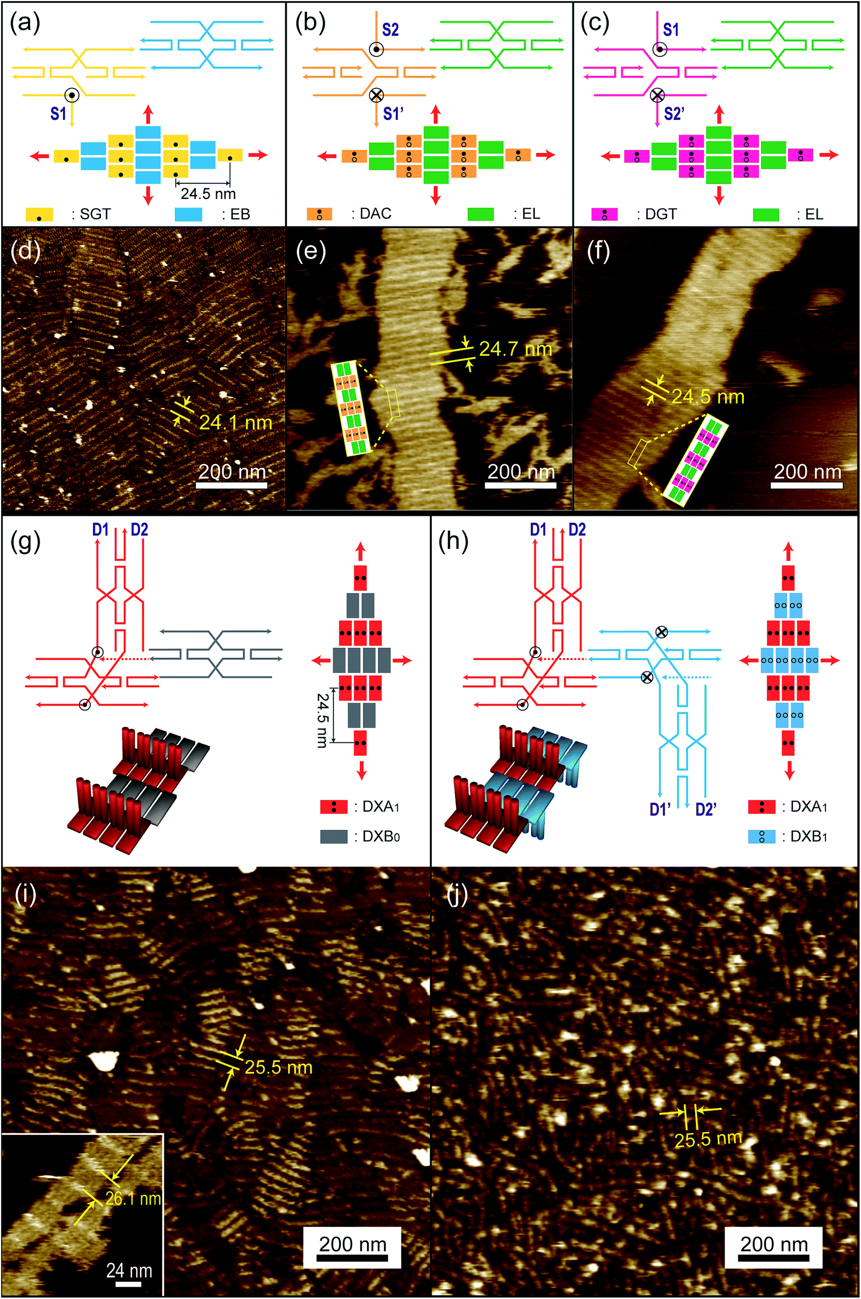 | ||
| Fig. 2 Schematic representations and AFM analysis of tiles involved in multi-layer assembly. (a) Layering tile SGT with pillar strand S1 protruding upwards (shown as a circle with a black dot) and connector tile EB are shown in yellow and blue respectively for base layer assembly. (b) Layering tile DAC with pillar strands S2 protruding upwards (shown as a circle with a dot), S1′ protruding downwards (shown as a circle with a cross mark) and connector tile EL shown in orange and green, respectively, for double-layer assembly. (c) Layering tile DGT with pillar strands S1 protruding upwards, S2′ protruding downwards and connector tile EL shown in pink and green, respectively, for multi-layer assembly. (d)–(f) Surface topology of single layers. (d) AFM image showing bright stripes due to formation of base layer consisting of SGT with single-side pillar strand protruding up and EB tiles via mica-assisted growth. (e) AFM image showing bright stripes due to the formation of a single layer made of DAC and EL tiles via free-solution annealing. (f) AFM image showing bright stripes due to formation of a single layer consisting of DGT and EL tiles via free-solution annealing. The average stripe distance measured in each case was of 24.1, 24.7 and 24.5 nm, respectively, which are similar to the expected value of 24.5 nm. (g) Layering tile DXA1 with DXB0 connector tile containing D1 and D2 sticky-ends protruding upwards (as black circles), shown in red and grey respectively, forming a single layer. (h) Layering tiles DXA1 with DXB1 containing D1′ and D2′ sticky-ends protruding downwards (as crossed circles), shown in red and blue respectively, forming double and multi-layered structures. Here sticky-ends D1 and D2 of DXA1 are complementary to sticky-ends D1′ and D2′ of DXB1. (i and j) Surface topology of single-layers. (i) Base layer formation with DXA1 and DXB0 tiles grown on mica; inset shows the base layer formed via free-solution annealing. (j) Single layers with DXA1 and DXB1 tiles obtained via mica-assisted growth. The red arrows in the schematics depict the direction of the lattice growth. | ||
The second type of tiles used included connector tiles consisting of DX tiles with sticky ends complementary to those of the layering tiles in such a manner as to link to the appropriate layering tiles and extend to form layers. The connector tiles are shown as an EB tile (extension base) in blue for the base layer and an EL (extension layer) in green for double- and multi-layer tiles [Fig. 1-(a) and 2-(a)–(c)]. All of these tile sets are in fact modified forms of R- and S-type DX tiles.6 Here, R- and S-type tiles have opposite 5′–3′ directionalities in their strands, as shown in Tables S1 and S3 of the ESI.† Thus the SGT, SAC, DAC and DGT tiles are modifications of the R-type DX tiles while the EB, EL tiles are modifications of the S-type DX tiles. The pillar strands are shown as S1 in SGT, S1′ and S2 in DAC, and S2′ and S1 in DGT, as shown in Fig. 2-(a)–(c), respectively (See ESI Tables S1† and S2† for schematics of the different tiles, with their respective strands, involved in multi-layer assembly via single-strand design. In addition, see Fig. S1,† a 2% agarose gel image showing association complexes of various DNA tiles in order to check the purities.). Here, the S1 and S2 sequences are designed to be complimentary to S1′ and S2′, respectively. Consequently, both tile types adhere in an alternating upside down orientation with respect to each other since they have opposite directionalities. In turn, the latter imparts an overall growth to the crystal that occurs in all directions once the nucleation process is initiated, as shown with red arrows in Fig. 2.
The design scheme adopted for fabricating multilayer nanostructure formed via DX tile-based design also involved the construction of multi-layered structures in a stepwise manner, commencing from the base layer followed by a double layer to finally form a multi-layered structure. As in previous designs, this scheme also employed layering and connector tiles. To design the layering tiles, two normal DX tiles were arranged perpendicular to each other such that one DX tile was positioned exactly in the centre, facing either up or down vertically, and protruding from the top of the previous tile to form the shape of the letter T. Connector tiles used here had same function as in the previous design to link and extend the layering tiles. Here, the layering tiles consist of DXA1 (double-crossover A1) in red and DXB1 (double-crossover B1) in blue while the connector tile consists of DXB0 (double-crossover B0) in grey, as shown in Fig. 1-(a), 2-(g) and (h) (see ESI Tables S2 and S3† for schematics of the different tiles with their respective strands involved in the multi-layer assembly via DX tile-based design). The D1, D2 and D1′, D2′ in DXA1 and DXB1 layering tiles are the sticky-ends which are complementary to each other for layer growth while the red arrows depict the direction of the lattice growth shown in Fig. 2-(g) and (h).
In our experiment, we sequentially fabricated layered nanostructures starting from the construction of a base layer, then a double-layer, and finally multiple layers. Each layer-by-layer assembly was imaged using AFM and verified via section analysis. We adopted the mica-assisted growth (MAG) method to construct the base layer while multi-step annealing methods were used to construct the double- and multi-layered structures. The MAG method was employed to obtain a fully covered base layer on the mica with larger crystal domain sizes29–32 relative to those prepared via solution annealing. Doing so helped not only during tile seeding and growth of the upper layers but also aided to distinguish the layer boundaries [Fig. 1-(c)]. In order to obtain full coverage on a given substrate, the DX tiles for the base layers (SGT and EB for single strand-based and DXA1 and DXB0 for DX tile-based designs) have to be larger than the specific critical concentration of 20 nM. In our experiment, we used 50 nM of DX tile for both base layers, and this was enough to ensure full coverage.
The schematics to form base layers with single strand-based designs are shown in Fig. 2-(a)–(c). In the AFM images, the single-strand pillar strands protruding either in one (in case of the SGT tile) or on both sides (in case of DAC and DGT tiles) can be observed as bright stripes in Fig. 2-(d)–(f), respectively. These lattices appeared to have periodic stripes along the duplex, although the arrangement of crystal domains was random. The spacing between the stripes in such cases was of 24.1 ± 0.2, 24.7 ± 0.2 and 24.5 ± 0.2 nm, respectively, which is in good agreement with the theoretically designed inter-junction distance of 24.5 nm, indicating that the structures formed as designed. Normally, the heights, i.e., thickness of the DX lattices – with a single duplex diameter of 2 nm in solution – were 1.2 nm due to the presence of the charged surface. Consequently, the height measured from the mica surface to the top of the pillar strands was of approximately 1.8 nm and 2.5 nm for SGT and DAC/DGT tiles, respectively, which were slightly larger than the single duplex thickness on the substrate.
We designed another base layer via DX tile-based design by adopting two approaches. First, we used a layering tile (DXA1) along with a connector tile (DXB0) for the base layer, and second, we used layering tiles (DXA1 and DXB1) without the connector tiles for double- and multi-layer formation. The schematics of the single layer formation through DX tile-based design without and with connector tiles are shown in Fig. 2-(g) and (h). The AFM images in Fig. 2-(i) and (j) show the formation of single layers made of the DXA1 tile with and without using a DXB0 connector tile, respectively. In the latter case, the DXB1 tile, which was designed to be complementary to the DXA1 tile, was used. Both images show a stripe distance of 25.5 nm, which is almost equivalent to the inter-junction distance of 24.5 nm of the design, confirming that the structures formed as designed. Interestingly, we couldn't observe evidence of multi-layered structures constructed by DXA1 and DXB1 tiles grown on mica, although multi-layered structures could be formed by the design. In order to grow multi-layer structures from these single layers without connector tiles, we add layer tiles (DXA1 and DXB1) later after forming the base layers on the substrate, as discussed below [Fig. 3-(f)].
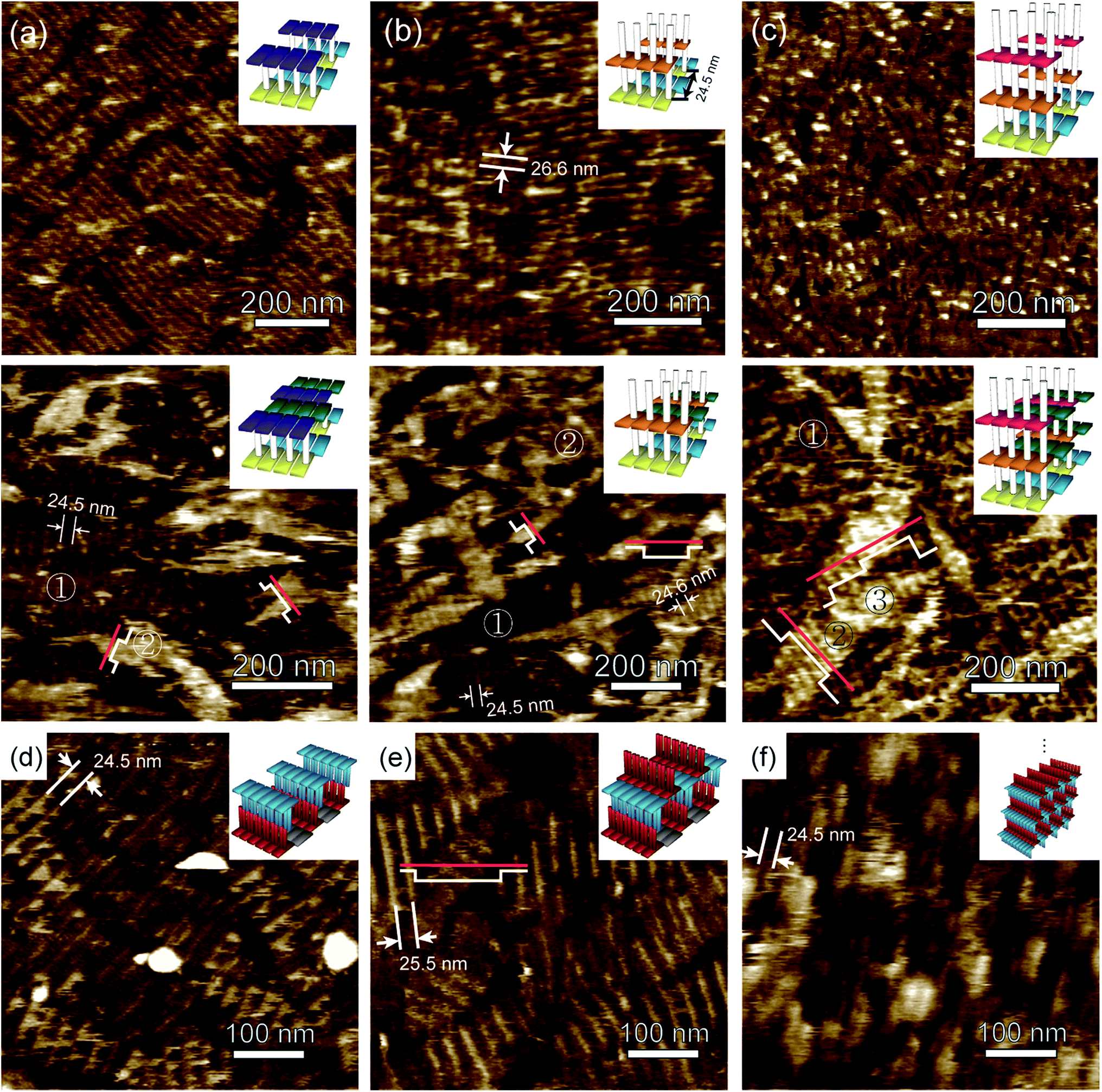 | ||
| Fig. 3 AFM images of double- and multi-layer assemblies of single-strand and DX tile-based design using layering tiles without and with connector tiles. The top and bottom panels in (a) show AFM images of double-layer assemblies formed with SGT and SAC tiles without and with connector EL tiles. The single and double layers are distinguishable by the colour contrast and are marked with ① and ②, respectively, in (a) the bottom panel. The stripes in the base layer with an average distance of 24.5 nm are similar to the expected value and can also be seen. The height profile analysis of the double layers (white line) based on the cross section of the red line shows a step height difference of ∼2.3 nm. The top and bottom panels in (b) show AFM images of the double-layer assembly consisting of DAC and SGT without and with connector EL. In the top panel (b) the intermolecular junction distance between the two pillar strands are shown as bright stripes and was measured as 26.6 nm, whereas the expected value was of 24.5 nm. The bottom panel (b) shows two distinct layers indicated by ① for the base layer and ② for the second layer. The height profile analysis of the double layers (white line) based on the cross section of the red line shows a step height difference of ∼2.0 nm. Spacing between the pillar strands for both the single- and double-layers was 24.5 and 24.6 nm respectively justifying the original design. The top and bottom panel in (c) shows AFM images of multi-layer assembly comprised of SGT, DGT and DAC without and with connector EL respectively. In the top panel (c), pillar strands appear inconspicuous while in the bottom panel (c), three distinct layer assemblies can be observed as represented by ①, ② and ③. The height profile analysis of the three layers (white line) based on the cross section of the red line shows a step height difference of 1.8 ± 0.2 nm, 2.5 ± 0.2 nm, and 3.0 ± 0.2 nm for single, double, and triple layers, respectively. (d)–(f) shows AFM images of double-layer assembly without and with DXA1 at a second layer and multi-layer assembly respectively. (d) AFM image of double-layer formation using DXA1, DXB0, and DXB1 tiles. The distance measured between the intermolecular junctions is 24.5 nm. (e) AFM image of the double-layer formation using another set of layering DXA1 tiles. White line represents the profile height along the cross section indicated by red line. The step height distance is ∼2.9 nm measured from top of the second layer, while the measured distance between the intermolecular junctions of adjacent tiles is ∼25.5 nm. (f) AFM image of multi-layer assembly comprised of layered DXA1 and DXB1 tiles. The distance between the DX junctions was measured as ∼24.5 nm. The colour scheme is kept the same as in Fig. 2, and the SAC tile is shown in dark blue. The insets represent the cartoon illustration for double- (without DXA1 at second-layer), double- (with DXA1 at second-layer) and multi-layer assemblies. | ||
We further synthesized double layers via single strand-based design employing a multi-step annealing method. For this, we adopted approaches similar to those used in the case where base layers used DX tile-based design. We then used AFM imaging to compare the results of both approaches. Fig. 3-(a) and (b), top panel, shows AFM images of layering tiles only, while the bottom panel shows AFM images for both layering and connector tiles at the second layer. The AFM images [Fig. 3-(a) and (b)] in the top panel show a bright striped pattern due to the binding of SAC and DAC tiles to the pillar strands, but we cannot observe the formation of the double layers due to the absence of connectors. We assume that these bright stripes are in fact pillar strands of the SAC tiles binding to their complementary strands on the SGT tiles (Fig. 3-(a)) and upward protruding pillar strands of the DAC tiles [Fig. 3-(b)]. We measured the distance between these bright stripes to confirm our assumption, and the distance of 26.6 nm showed that the structures that formed were in good agreement with the theoretical design.
To get a better picture, distinguishable single and double layers were observed when the EL connector tile was used along with the SAC tile, as indicated by the ① and ② symbols, respectively, in Fig. 3-(a, bottom panel). We then performed a height profile analysis (white line) based on the cross-section of the red line, which showed a step height difference of ∼2.3 nm between the layers and further confirmed that a double-layer structure had formed. This height measurement didn't match with the height of the pillar strands between the layers, which theoretically should be of around 10.2 nm (30 nucleotides in length). This discrepancy among the measured and the theoretical height can be possibly attributed to the fact that the DNA double helix (formed by pillar strands) is not a relatively rigid structure and tends to flatten out on the mica surfaces during AFM imaging due to the suppression by electrostatic interactions between the negatively charged DNA molecules and the charged mica substrate.11,33,34 Hence, there might be certain limitations to precisely measure the heights of the single strands, and thus, the measured height would always be less than the theoretically predicted height.35,36 In contrast, the centre-to-centre inter-junction distance in the first layer was measured to be of around 24.5 nm, which is consistent with the theoretical design. The difference between the layers was also noticeable as bright and dark areas, marked as ② and ① respectively.
The AFM image shown in Fig. 3-(b, bottom) depicts a distinct layer assembly when the EL connector tile was used along with a DAC tile. This image is comparable to the image shown in Fig. 3-(a, bottom) in terms of the height of the double-layer and the colour contrast between the layers. The height profile analysis (white line) is based on the cross-section of the red line showing a step height difference of ∼2.0 nm between the layers. However, the periodic bright stripes of the top layer were more evident in this case, probably as a result of the presence of an upward protruding pillar strand. The inter-junction spacing between the stripes was measured as 24.6 nm, which was similar to the first layer and consistent with the theoretical design.
To fabricate multiple layers with a single strand-based design, we again used the multi-step annealing method, and the same two design approaches were applied to construct multi-layers by layering tiles with or without connector tiles. The AFM image in Fig. 3-(c) shows an example of a multi-layer assembly using two distinct layer tiles, DAC and DGT, each with both upward and downward protruding pillar sticky ends but without the connector EL tile. Here, bright stripes were seen but were inconspicuous in some regions, which is likely a consequence of the base layers flipping on the mica. When the DAC and DGT tiles were used with the connector EL tiles, as shown in the AFM image in Fig. 3-(c, bottom), a distinct layer assembly was observable, as shown with ①, ② and ③ symbols that indicate the first, second, and third layers, respectively.
The first-layer was identifiable by stripes that formed due to pillar sticky-ends of the SGT tiles. The second layer appeared as brighter small patches on top of the first layer, followed by the third layer that formed as white tiny regions overlapping the second layers. Nevertheless, the third layers barely formed lattices, but instead were prominently seen as small white regions that perhaps might have been lattices with a small number of tiles. It was interesting to note that the coverage by the upper layers was smaller than that of the lower layers, so we could identify the layers by observing the contrast in the images. The height profile analysis for these multi-layered structures [white line in Fig. 3-(c) bottom] according to the cross section of the red line shows a step height difference of ∼1.8 ± 0.2 nm, 2.5 ± 0.2 nm, and 3.0 ± 0.2 nm for the first, second, and third layers, respectively. This indicates that the single-layer heights of roughly 0.6 nm above the base layers were discrete.
According to the design, the theoretical heights of these layered structures should be of 2.0 + 10.2 nm for the first layer with a single pillar sticky-end, 4.0 + 20.4 nm for the second layer with double pillar sticky-ends, and 6.0 + 30.6 nm for the third-layer with double pillar sticky-ends. However, the height differences observed were different by about an order of magnitude, and this may be a result of the suppression of flexible pillar strands by the strong electrostatic interactions between the DNA molecules and the mica substrate, as mentioned earlier. Certainly the formation of multi-layered nanostructures was easily distinguishable when connector tiles were added between the layering tiles due to the relative structural stability.
Furthermore, we performed experiments to design double- and multi-layer nanostructures via DX tile-based design through multi-step annealing. DXA1, DXB0 and DXB1 tiles were used to assemble the structures shown in Fig. 3-(d). Here, DXA1 and DXB0 tiles were used as base layers, and DXB1 for double layers. Thus, the platform with double layers was achieved by using DXB1, which has complimentary sticky-ends with DXA1. As shown in the AFM image in Fig. 3-(d), bright stripes were observed with spacing between them of 24.5 nm, which is in good agreement with the theoretical inter-junction distance of the DX tiles. About half of the regions of stripes due to the binding of DXB1 to DXA1 were clearly visible, whereas others were not due to DXA1 in the base layers flipping on the mica. Also the height difference between such contrast areas was measured to be of ∼1.9 nm which indicates that the appropriate structures had been formed. Subsequently, we assembled double-layers by adopting a multi-step annealing method. Here, after forming structures on mica, as shown in Fig. 3-(d), we added them into a test tube containing pre-annealed DXA1 tiles. Fig. 3-(e) reveals the AFM image of the double layers with its properly formed geometry. The height profile analysis of the layers from the second layer [white line in Fig. 3-(e)] based on the cross section of the red line shows a step height difference of ∼2.2 nm.
To grow multi-layered structures, we added base layers that had formed with DXA1 and DXB1 tiles on mica [Fig. 2-(j)] into pre-annealed DXA1 and DXB1 tiles, as shown in Fig. 3-(f). The topological difference of the multi-layered structures was observed as through the periodic lines along a line perpendicular to the duplex axis with various heights when compared to the double layers as shown in Fig. 3-(d) and (e). This might have been a result of the vertically standing and partially covered layers forming from DXA1 and DXB1, thereby masking the bottom layers. Although there are certain limitations to estimating the number of layers due to the non-uniform height of the layers, the average number of layers can be estimated through the use of the scratch method with the AFM contact mode, which produces a height profile from the base. In our case we noticed the average height after the scratch was of about 9.5 nm from base layers, which meant that about 5 layers had formed in this design, as shown in Fig. S2,† ESI.
Conclusions
We demonstrate the fabrication of multi-layered nanostructures through single strand-based and DX tile-based design with the aid of MAG and multi-step annealing methods. The heights of the multi-layered nanostructures were less than that predicted from the design, which might arise as a consequence of the suppression of flexible pillar strands or DX duplexes by electrostatic interactions between the DNA molecules and the mica substrate. Nevertheless, the use of layering tiles in combination with connector tiles provided stability in the layered structures and helped form the structures expected in our design scheme. This kind of stepwise multi-layer assembly might bear an added benefit since various layers can be packed within 3D structures, providing various spacing sizes to incorporate guest molecules.13,37 Alternatively, one might envision the use of vertically standing pillar strands as anchors to align biomolecules3,28 or to attach various types of functionalized nano- and bio-materials27,38–40 in parallel arrays along the surfaces.Acknowledgements
This work was supported by the National Research Foundation of Korea (NRF), funded by the Ministry of Science, ICT & Future Planning of the Korean government (MSIP) (NRF-2014R1A2A1A11053213, NRF-2012M3A7B4049801, & CAMM-2014M3A6B3063707).Notes and references
- N. C. Seeman, J. Theor. Biol., 1982, 99, 237–247 CrossRef CAS.
- P. Yin, R. F. Hariadi, S. Sahu, H. M. T. Choi, S. H. Park, T. H. LaBean and J. H. Reif, Science, 2008, 321, 824–826 CrossRef CAS PubMed.
- H. Yan, S. H. Park, G. Finkelstein, J. H. Reif and T. H. LaBean, Science, 2003, 301, 1882–1884 CrossRef CAS PubMed.
- P. W. K. Rothemund, Nature, 2006, 440, 297–302 CrossRef CAS PubMed.
- Y. Ke, L. L. Ong, W. M. Shih and P. Yin, Science, 2012, 338, 1177–1183 CrossRef CAS PubMed.
- P. W. K. Rothemund, N. Papadakis and E. Winfree, PLoS Biol., 2004, 2, 2041–2053 CAS.
- W. M. Shih, J. D. Quispe and G. F. Joyce, Nature, 2004, 427, 618–621 CrossRef CAS PubMed.
- F. Mathieu, S. P. Liao, J. Kopatsch, T. Wang, C. D. Mao and N. C. Seeman, Nano Lett., 2005, 5, 661–665 CrossRef CAS PubMed.
- R. P. Goodman, I. A. T. Schaap, C. F. Tardin, C. M. Erben, R. M. Berry, C. F. Schmidt and A. J. Turberfield, Science, 2005, 310, 1661–1665 CrossRef CAS PubMed.
- S. M. Douglas, J. J. Chou and W. M. Shih, Proc. Natl. Acad. Sci. U. S. A., 2007, 104, 6644–6648 CrossRef CAS PubMed.
- Y. He, T. Yel, M. Su, C. Zhang, A. E. Ribbe, W. Jiang and C. D. Mao, Nature, 2008, 452, 198–202 CrossRef CAS PubMed.
- J. Zimmermann, M. P. J. Cebulla, S. Mönninghoff and G. von Kiedrowski, Angew. Chem., Int. Ed., 2008, 47, 3626–3630 CrossRef CAS PubMed.
- R. P. Goodman, M. Heilemann, S. Doose, C. M. Erben, A. N. Kapanidis and A. J. Turberfield, Nat. Nanotechnol., 2008, 3, 93–96 CrossRef CAS PubMed.
- J. Chen and N. C. Seeman, Nature, 1991, 350, 631–633 CrossRef CAS PubMed.
- Y. Zhang and N. C. Seeman, J. Am. Chem. Soc., 1994, 116, 1661–1669 CrossRef CAS.
- F. A. Aldaye and H. F. Sleiman, J. Am. Chem. Soc., 2007, 129, 13376–13377 CrossRef CAS PubMed.
- F. A. Aldaye, P. K. Lo, P. Karam, C. K. McLaughlin, G. Cosa and H. F. Sleiman, Nat. Nanotechnol., 2009, 4, 349–352 CrossRef CAS PubMed.
- S. M. Douglas, H. Dietz, T. Liedl, B. Hogberg, F. Graf and W. M. Shih, Nature, 2009, 459, 414–418 CrossRef CAS PubMed.
- E. S. Andersen, M. Dong, M. M. Nielsen, K. Jahn, R. Subramani, W. Mamdouh, M. M. Golas, B. Sander, H. Stark, C. L. P. Oliveira, S. Jan, V. Pedersen, F. Bikedal, K. V. Besenbacher, J. Gothelf and J. Kjems, Nature, 2009, 459, 73–76 CrossRef CAS PubMed.
- J. Zheng, J. J. Birktoft, Y. Chen, T. Wang, R. Sha, P. E. Constantinou, S. L. Ginell, C. Mao and N. C. Seeman, Nature, 2009, 461, 74–77 CrossRef CAS PubMed.
- U. Majumder, A. Rangnekar, K. V. Gothelf, J. H. Reif and T. H. LaBean, J. Am. Chem. Soc., 2011, 133, 3843–3845 CrossRef CAS PubMed.
- Y. H. Roh, R. C. Ruiz, S. Peng, J. B. Lee and D. Luo, Chem. Soc. Rev., 2011, 40, 5730–5744 RSC.
- L. R. Nathaniel and C. A. Mirkin, Chem. Rev., 2005, 105, 1547–1562 CrossRef PubMed.
- M. R. Hartman, R. C. Ruiz, S. Hamada, C. Xu, K. G. Yancey, Y. Yu, W. Han and D. Luo, Nanoscale, 2013, 5, 10141–10154 RSC.
- N. C. Seeman, Annu. Rev. Biochem., 2010, 79, 65–87 CrossRef CAS PubMed.
- R. Amin, A. Kulkarni, T. Kim and S. H. Park, Curr. Appl. Phys., 2011, 12(3), 841–845 CrossRef PubMed.
- J. D. Le, Y. Pinto, N. C. Seeman, K. Musier-Forsyth, T. A. Taton and R. A. Kiehl, Nano Lett., 2004, 4, 2343–2347 CrossRef CAS.
- E. Winfree, F. Liu, L. A. Wenzler and N. C. Seeman, Nature, 1998, 394, 539–544 CrossRef CAS PubMed.
- J. Lee, S. Kim, J. Kim, C. W. Lee, Y. Noh and S. H. Park, Angew. Chem., Int. Ed., 2011, 50, 9145–9149 CrossRef CAS PubMed.
- X. Sun, H. S. Ko, C. Zhang, A. E. Ribbe and C. J. Mao, J. Am. Chem. Soc., 2009, 131, 13248 CrossRef CAS PubMed.
- S. Hamada and S. Murata, Angew. Chem., Int. Ed., 2009, 48, 6820–6823 CrossRef CAS PubMed.
- B. Kim, R. Amin, J. Lee, K. Yun and S. H. Park, Chem. Commun., 2011, 47, 11053–11055 RSC.
- D. Han, S. Pal, J. Nangreave, Z. Deng, Y. Liu and H. Yan, Science, 2011, 332, 342–346 CrossRef CAS PubMed.
- Z. Li, M. Liu, L. Wang, J. Nangreave, H. Yan and Y. Liu, J. Am. Chem. Soc., 2010, 132, 13545–13552 CrossRef CAS PubMed.
- J. Lee, R. Amin, B. Kim, S. Kim, C. W. Lee, J. M. Kim, T. H. LaBean and S. H. Park, Soft Matter, 2012, 8, 44–47 RSC.
- B. Kim, S. Jo, J. Son, J. Kim, M. H. Kim, S. U. Hwang, S. R. Dugasani, B. D. Kim, W. K. Liu, M. K. Kim and S. H. Park, Nanotechnology, 2014, 25, 105601 CrossRef PubMed.
- C. M. Erben, R. P. Goodman and A. J. Turberfield, Angew. Chem., 2006, 45, 7414–7417 CrossRef CAS PubMed.
- S. Pal, Z. Deng, B. Ding, H. Yan and Y. Liu, Angew. Chem., Int. Ed., 2010, 49, 2700–2704 CrossRef CAS PubMed.
- K. Keren, R. S. Berman, E. Buchstab, U. Sivan and E. Braun, Science, 2003, 302, 1380–1382 CrossRef CAS PubMed.
- H. T. Maune, S. P. Han, R. D. Barish, M. Bockrath, W. A. Goddard III, R. W. K. Rothermund and E. Winfree, Nat. Nanotechnol., 2010, 5, 61–66 CrossRef CAS PubMed.
Footnotes |
| † Electronic supplementary information (ESI) available: Schematic diagram and DNA sequences for tiles forming single-, double- and multi-layers; height profiles of multi-layer assembly; a 2% agarose gel image. See DOI: 10.1039/c5ra03477a |
| ‡ These authors contributed equally to the paper. |
| This journal is © The Royal Society of Chemistry 2015 |