Enhancement of solar cell efficiency using perovskite dyes deposited via a two-step process

Thanh-Tung Duongac, Yun-Jeong Kima, Ji-Ho Eoma, Jin-Seok Choiab, Anh-Tuan Lec and Soon-Gil Yoon*a
aDepartment of Materials Science and Engineering, Chungnam National University, Daeduk Science Town, 305-764, Daejeon, Korea. E-mail: sgyoon@cnu.ac.kr
bResearch Analysis Center, Korea Advanced Institute of Science and Technology, 291 Daehak-ro, Yuseong-gu, 305-701, Daejeon, Korea
cDepartment of Nanoscience and Nanotechnology, Advanced Institute of Science and Technology (AIST), Hanoi University of Science and Technology (HUST), 01 Dai Co Viet, Hai Ba Trung, Hanoi, Vietnam

Received 23rd February 2015 , Accepted 30th March 2015

First published on 30th March 2015


Abstract

This study examined the effect of different thick-compact-TiO2 blocking layers (c-TiO2) and mesoporous-TiO2 layers (m-TiO2) on the efficiency of perovskite cells. Anatase c-TiO2 layers with different thicknesses were in situ deposited onto a FTO/glass substrate at a temperature of 400 °C via nano-cluster deposition (NCD). The 80 nm-thick c-TiO2 layers were deposited with good step-coverage on the rough-FTO surface, and were in situ crystallized via an anatase phase. The perovskite cells with 80 nm-thick c-TiO2 and 600 nm-thick-m-TiO2 layers showed the highest photovoltaic parameters: JSC of 21.0 mA cm−2, VOC of 0.89 V, FF of 62%, and efficiency (η) of 11.5%. For enhancement of the cell efficiency, solar cells with bi-layer perovskite dyes were deposited via a two-step process onto the m-TiO2 layer (200 nm)/TiO2 blocking layers (80 nm) and showed VOC and FF values of approximately 1.06 and 64%, respectively, with a maximum photo-conversion efficiency of approximately 14.2%.

1. Introduction

CH3NH3PbX3 perovskite (X = Cl, Pb, I) has a direct band gap energy that ranges from 1.5–2 eV and has shown outstanding properties as an absorber layer in perovskite solar cells, with improvements from 3.8 to more than 19.3% in the past 4 years, and has been identified as a possible base material for high-efficiency commercial photovoltaics.1–6 A typical perovskite solar cell includes a perovskite absorbing layer sandwiched between the electron and hole transport layers (ETL, HTL, respectively). To achieve a high photoelectrical conversion efficiency (PCE), the density of the trapping and recombination centers of the absorber must be relatively low in order to enhance the carrier transport pathways to both the ETL and the HTL.7 Spiro-OMeTAD has commonly been used as the HTL, with a conductivity that is 10 times higher than that of the ETL, resulting in unnecessary ohmic losses, which were mainly caused by the ETL.8 The ETL includes a c-TiO2 blocking layer with and without a mesoporous scaffold layer. With a scaffold layer, perovskite solar cells with an efficiency of >12% can be used for thin film planar structures, meso-superstructures, mesoporous structures, and to achieve a bi-layer architecture. The choice of using a perovskite solar cell structure either with or without a scaffold layer depends on the carrier diffusion length of the dye material.9–12 Because CH3NH3PbI3 perovskite dyes with a carrier diffusion length of ∼100 nm were too for collecting contacts, either a mesoporous or a bilayer structure is required where n-type semiconductors (ZnO and TiO2)13,14 are employed as an electron conduction pathway. In the case of CH3NH3PbClxI3−x, the carrier's diffusion length is >1000 nm, and the absorber layer itself can generate both electrons and holes and transport them to the collecting contacts. The semiconducting scaffold layer can then be replaced by an insulating mesoporous scaffold layer (ZrO2 and Al2O3),15,16 which is referred to as a meso-superstructure, or can be used without a scaffold layer, which is referred to as a thin-film planar structure.17 The hole-blocking layer is used to prevent holes that form in the perovskite or HTL layer from reaching the fluorine-doped tin oxide (FTO) electrode, as this would short-circuit the cell. Blocking layers require a low contact resistance at the interface between the conductive film of a working substrate and the TiO2 as well as a high charge-transfer resistance at the TCO–HTL interface. Yang et al. demonstrated an improvement in cell efficiency of from 13.8 to 16.5% by using Y-doped TiO2 in order to increase carrier concentrations. In their demonstration, they emphasized the importance of a blocking layer in perovskite solar cells.7 The blocking layer is typically composed of c-TiO2 that typically is prepared by spin coating or spray pyrolysis using a titanium precursor solution. However, with these methods, it is difficult to control uniformity and thickness on a nano-scale.18–22

Uniform and pinhole-free c-TiO2 layers have been prepared using atomic layer deposition (ALD) to improve device performance.23 However, the ALD method had drawbacks that included a low crystallinity of the films due to a low deposition temperature. Therefore, in order to enhance the crystalline quality of the blocking layers, a new deposition method should be considered. In previous studies, SnO2 and Zn-doped TiO2 thin films deposited by NCD were employed as a blocking layer to enhance DSSC performance, and NCD allowed depositions with high crystallization, uniformity, and an easily controlled thickness.24–26

In the present study, the structural and electrical properties of the crystallized c-TiO2 layers deposited onto FTO/glass at a low temperature of 400 °C by NCD were investigated at different c-TiO2 and m-TiO2 thicknesses. For enhanced efficiencies of the perovskite solar cells, different processes were used for the preparation of perovskite dyes using c-TiO2 blocking layers prepared by different processes. The thicknesses of the m-TiO2 and c-TiO2 layers were maintained at 200 and 80 nm, respectively.

2. Experimental details

2-1 Preparation of the c-TiO2 blocking layers by NCD

For deposition of the c-TiO2 blocking layer using NCD, the Ti(O-iPr)2(dibm)2(Ti(Oi-C3H7)2(C9H15-O2)2) precursors that were used for the liquid delivery process were dissolved in hexane and used as the sources of titanium at concentrations of 0.075 M. When the chemical sources entered the vaporizer, they were immediately vaporized and carried to the showerhead within the reaction chamber via argon carrier gas at a flow rate of 100 sccm (standard cm3 min−1). The oxygen was supplied to the showerhead as a reaction gas at a fixed flow rate of 100 sccm. The showerhead temperature was maintained at 240–300 °C, while the substrate temperature was maintained at 400 °C for crystallization of the c-TiO2. The film thicknesses of 20, 40, 60, 80, and 100 nm were estimated using the deposition rate of the TiO2 (∼10 nm min−1), and their real thicknesses were confirmed through cross-sectional images using scanning electron microscopy (SEM) and transmission electron microscopy (TEM). The 200, 400, 600, and 800 nm-thick m-TiO2 layers were deposited onto the TiO2 blocking layer/FTO substrates via spin coating at 2000 rpm (revolutions per minute) using the TiO2 paste (Dyesol 18NR-T) diluted further in methanol at ratios of 1[thin space (1/6-em)]:[thin space (1/6-em)]10, 1[thin space (1/6-em)]:[thin space (1/6-em)]7, 1[thin space (1/6-em)]:[thin space (1/6-em)]5, and 1[thin space (1/6-em)]:[thin space (1/6-em)]3 by weight. The layers were sintered under an air atmosphere at 450 °C for 1 h.

2-2 Preparation of the c-TiO2 blocking layer using the conventional method

A conventional c-TiO2 blocking layer was prepared as follows. The clean substrates were spin-coated with 0.15 M titanium diisopropoxide bis(acetylacetonate) (Aldrich) at 3000 rpm for 30 s to achieve a thickness of 80 nm. After drying at 125 °C for 10 min, they were sintered at 550 °C for 15 min under an air atmosphere.

2-3 Preparation of m-TiO2 layers onto the c-TiO2 blocking layer

The 200, 400, 600, and 800 nm-thick m-TiO2 layers were deposited onto the TiO2 blocking layer/FTO substrate via spin coating at 2000 rpm using the TiO2 paste (Dyesol 18NR-T) diluted further in methanol at ratios of 1[thin space (1/6-em)]:[thin space (1/6-em)]10, 1[thin space (1/6-em)]:[thin space (1/6-em)]7, 1[thin space (1/6-em)]:[thin space (1/6-em)]5, and 1[thin space (1/6-em)]:[thin space (1/6-em)]3 by weight. The layers were sintered under an air atmosphere at 450 °C for 1 h.

2-4 Preparation of the perovskite dyes onto the m-TiO2/c-TiO2/FTO/glass

For preparation of the perovskite dye (CH3NH3PbI3), two approaches were undertaken in the present study.

First, in a single-step, CH3NH3I was synthesized by reacting 24 mL of methylamine (33 wt% in absolute ethanol, Sigma) and 10 mL of hydroiodic acid (57 wt% in water, Aldrich) in a 250 mL round-bottom flask at 0 °C for 2 h with stirring. The precipitate was recovered by placing the solution onto a rotary evaporator and carefully removing the solvents at 50 °C. The raw product, CH3NH3I, was re-dissolved in 80 mL absolute ethanol and precipitated with the addition of 300 mL diethyl ether. After filtration, the step was repeated, and the solid was collected and dried at 60 °C in a vacuum oven for 24 h. Then, 1.157 g of PbI2 and 0.395 g of CH3NH3I were dissolved in 2.0 mL γ-butyrolacetone solution at 60 °C. The clear perovskite precursor solution was first spread onto the m-TiO2 films for 5 s, which were then spun at 4000 rpm for 30 s under an air atmosphere via one-step spin coating. The deposited CH3NH3PbI3 films were finally dried on a hot-plate at 100 °C for 10 min.

Second, in a two-step process, solutions of 400 mg mL−1 PbI2 (Sigma) in N,N-dimethylformamide (DMF) were spin-coated onto the m-TiO2 (200 nm)/c-TiO2 (80 nm)/FTO substrates at 4000 rpm for 30 s, and dried at 110 °C for 15 min. The CH3NH3I powder was spread around the PbI2-coated substrates and covered with a Petri dish then heated at 150 °C for 2 h. Both the deposition of PbI2 film by spin coating and the deposition of CH3NH3I film by vapor treatment were performed under a N2 atmosphere. After cooling, the as-prepared substrates were washed with isopropanol, then dried, and annealed.

2-5 Preparation of the hole transport layers (HTL)

The HTLs were deposited onto the perovskite dye/m-TiO2/c-TiO2/FTO/glass via spin coating at 4000 rpm for 5 s using a hole transport solution (HTM) where a spiro-OMeTAD/chlorobenzene (180 mg/1 mL) solution was employed with the addition of 50 μL of Libis(trifluoromethanesulfonyl) imide (Li-TFSI, Sigma)/acetonitrile (170 mg/1 mL) and 20 μL tert-butylpyridine (tBP, Sigma).

2-6 Preparation of the Au electrode

Finally, for use as counter electrodes, the 100 nm-thick Au films as were deposited by dc (direct current) sputtering under a working pressure of 0.4 Pa (at a base pressure of 6.6 × 10⁻³ Pa) using a gold target with a 2 inch diameter. The active area of the cell was approximately 0.25 cm−2. After deposition of the Au layer, the cells were annealed at 100 °C for 10 min to promote a strong adhesion between the Au and the HTL.

2-7 Characterization of the perovskite solar cells

The surface morphologies of c-TiO2, m-TiO2, and perovskite dyes were analyzed via SEM (TOPCON DS-130C). The cross-sectional images and crystallinity of the c-TiO2 layers were observed via high-resolution TEM (HRTEM, JEM-2100F, HR). The samples were mounted on an aperture grid and mechanically polished to 2–3 microns in thickness. Finally, TEM samples were prepared after ion milling for a short period of time. The optical transmittance of the as-deposited c-TiO2 films was measured using S-3100 UV-vis spectroscopy. The crystalline structure and the preferred orientation of the c-TiO2 and the perovskite dye films were characterized via X-ray diffraction (XRD, Rigaku D/MAX-RC) using Cu Kα radiation and a nickel filter. The photocurrent–voltage (IV) characteristics of the solar cells were measured using an IVIUMSTAT under illumination from a Sun 3000 solar simulator composed of 1000 W mercury-based Xe arc lamps and AM 1.5-G filters. Light intensity was calibrated with a silicon photodiode.

3. Results and discussion

3-1 Thickness effect of m-TiO2 and c-TiO2 on the efficiency of cells with perovskite dyes prepared via a single-step process

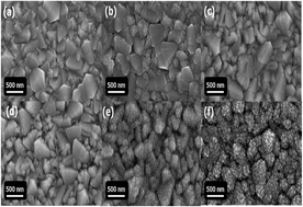
The SEM surface images of the bare-FTO and c-TiO2 films of various thicknesses are shown in Fig. 1. There were no significant morphological changes for 20 nm (Fig. 1(b)) and 40 nm-thick c-TiO2 (Fig. 1(c)) films. However, with the TiO2 (60 nm) films, small particles appeared on the FTO grains, as shown in Fig. 1(d). However, c-TiO2 films with thicknesses of 80 and 100 nm (see Fig. 1(e) and (f), respectively) could be uniformly deposited onto the FTO grains. The SEM images did not clearly show the morphologies of the c-TiO2 layers, but the 80 nm-thick c-TiO2 films grown onto FTO could be clearly observed using TEM. Fig. 2 shows the TEM cross-sectional and high-resolution images observed using 80 nm-thick c-TiO2 films grown onto the FTO. Fig. 2(a) shows the step-by-step coverage of the c-TiO2 films grown along the surface of the FTO grains, and Fig. 2(b) displays a cross-sectional image of the c-TiO2 film only. The TEM image of the c-TiO2 films shows that the 80 nm-thick c-TiO2 films were well deposited onto the FTO grains. The c-TiO2 films displayed a clear crystallinity, indicating an interplanar distance of d(101) = 0.352 nm, as shown in the HRTEM image in Fig. 2(c). HRTEM analysis confirmed that the c-TiO2 films were in an anatase phase. X-ray diffraction analysis was performed in order to ascertain the crystallinity of a larger area of the c-TiO2 films than what could be shown by TEM analysis. As shown in Fig. 2(d), the 80 nm-thick c-TiO2 films grown onto the FTO showed the clear crystallinity of an anatase phase, which exists at 2θ = 25.4°. Based on the XRD and TEM analysis, the c-TiO2 blocking layers were in situ crystallized in an anatase phase at a low temperature of 400 °C via NCD.
image file: c5ra03370e-f1.tif
Fig. 1 SEM surface images of (a) bare-FTO, (b) 20, (c) 40, (d) 60, (e) 80, and (f) 100 nm thick-c-TiO2 layers deposited at 400 °C by NCD onto the FTO/glass substrate.

image file: c5ra03370e-f2.tif
Fig. 2 TEM cross-sectional image of (a) c-TiO2 layer/FTO and (b) focused image of c-TiO2 layer. (c) High-resolution TEM image and (d) XRD pattern of 80 nm-thick-c-TiO2 layers grown onto the FTO/glass substrate.

To evaluate the crystallinity of the ultra-thin c-TiO2 films, the XRD analysis was limited and TEM analysis was used only to evaluate the local area. Therefore, the crystallinity required evaluation in both the ultra-thin and large-area sections of the c-TiO2 films. To investigate the relationship between the crystallinity and the thickness of c-TiO2 films, investigation of the bandgap energies of the films as a function of thickness replaced the XRD and TEM analyse. Fig. 3(a) shows the transmittance of the c-TiO2 blocking layers with different thicknesses as a function of wavelength. Transmittances of the c-TiO2 layers decreased with increasing thickness. However, the 40 to 100 nm-thick blocking layers exhibited a similar transmittance as that of 20 nm-thick blocking layers. The plot of (α)2 versus photon energy () was established, assuming that the transition is a direct one. The absorption coefficient (α) from the transmittance results of Fig. 3(a) was determined using the following relationship:

 
α = ln(1/T)/t (1)


image file: c5ra03370e-f3.tif
Fig. 3 (a) Transmittance of the c-TiO2 blocking layers with different thicknesses as a function of wavelength. (b) A plot of (α)2 versus photon energy for different thicknesses of c-TiO2 layers.

In that formula, T is the transmittance and t is the thickness of the films. A linear fit was made and is shown in Fig. 3. The bandgap energy (Eg) was obtained from the intercept with the energy axis, and the relationship between Eg and thickness is shown in the inset of Fig. 3(b). The bandgap energies of the films were decreased from 5.25 to 3.7 eV as the thickness increased from 20 to 40 nm, and they were maintained at 3.5 eV as the thickness was increased from 60 to 100 nm. These results suggested that the crystallinity of the c-TiO2 blocking layers increased as the thickness increased.

Fig. 4 shows the SEM cross-sectional images of different m-TiO2 thicknesses prepared on the c-TiO2 layers by spincoating. After deposition, m-TiO2 films were annealed at 500 °C for 1 h under an air atmosphere. The mesoporous films were well developed onto the c-TiO2/FTO, and their thicknesses were clearly identified at 200, 400, 600, and 800 nm. The effect on cell efficiency of different m-TiO2 thicknesses with a constant thickness of the c-TiO2 layer was addressed in the last section. Fig. 5(a) shows the SEM surface image of CH3NH3PbI3 perovskite dye deposited onto 600 nm-thick m-TiO2 films. The perovskite dye films were annealed at 100 °C for 10 min under a dry air atmosphere. That image shows that several micrometer-sized regular islands (called the capping layer) were densely formed on the top of the m-TiO2 films. The capping layer is important in determining the filling fraction and infiltration depth of the CH3NH3PbI3 and HTL into the m-TiO2, because these factors indicate whether the CH3NH3PbI3 nanocrystals are contacted by the HTL. Because the CH3NH3PbI3 dye showed small electron and hole diffusion lengths of ∼100 nm, the HTM which deeply penetrated into the m-TiO2-coated perovskite films is necessary for hole collection. Therefore, a capping layer with a porous density should be uniformly distributed onto the m-TiO2 layers. Fig. 5(b) and (c) shows the SEM images with the capping layer and the m-TiO2 layer without a capping layer, respectively. The capping layer (Fig. 5(a)) had a dense and homogeneous morphology, compared with the porous morphology of the m-TiO2 layer without a capping layer (Fig. 5(c)). Fig. 5(d) shows the large sizes of the irregular shapes of the capping layer formed on the 200 nm-thick-m-TiO2 layers. Based on the surface images of the capping layers, the density and shapes of the capping layers depended on the m-TiO2 thickness, suggesting the influence of the efficiency of the perovskite cells. The diffusion of the HTM solution into the m-TiO2 layers through the dense capping layer was very difficult. The HTM solution could penetrate through the porous m-TiO2 films and make contact with the bottom electrode. Therefore, the blocking layer is needed to prevent the HTM from making contact with the FTO.


image file: c5ra03370e-f4.tif
Fig. 4 SEM cross-sectional images of (a) 200, (b) 400, (c) 600, and (d) 800 nm-thick m-TiO2 layers deposited by spin coating onto a FTO substrate. They were annealed at 450 °C for 1 h under an air atmosphere.

image file: c5ra03370e-f5.tif
Fig. 5 (a) SEM surface images of the perovskite dye coated onto the 600 nm-thick-m-TiO2 layer. (b) and (c) Focused SEM image with a capping layer and with no capping layer, respectively. (d) SEM surface image of the perovskite dye coated onto a 200 nm-thick m-TiO2 layer. (e) XRD pattern of CH3NH3PbI3 perovskite dye annealed at 100 °C for 10 min under a dry air atmosphere.

To identify the crystallinity of the perovskite dye, it was coated onto the FTO/glass via spin coating. Fig. 5(e) shows the XRD pattern of the perovskite dye coated onto the FTO/glass. The annealed perovskite dye films showed good crystallinity with peaks at (110), (220), (310), and (224), which agreed well with the reported results.4,27

To demonstrate the effect of a c-TiO2 blocking layer on the efficiency of the perovskite cells, the current and voltage (JV) characteristics of the perovskite cells with different c-TiO2 thicknesses are shown in Fig. 6(a). The short-circuit current density (JSC) and open-circuit voltage (VOC) of the cells increased with increasing c-TiO2 thickness, representing the typical JV properties of perovskite cells. The 80 nm-thick c-TiO2 films showed the highest values for JSC and VOC at approximately 21.0 mA cm−2 and 0.89 V, respectively. However, 100 nm-thick c-TiO2 films showed decreases in JSC and VOC, compared with those of 80 nm-thick c-TiO2 films. Because a blocking layer was required to prevent the recombination of the electrons and holes, an optimal thickness was determined for the highest efficiency of the perovskite solar cells. The abrupt increase of the efficiencies in 60 and 80 nm-thick c-TiO2 blocking layers was attributed to the enhanced blocking of the recombination of the electrons and holes. However, the decrease in efficiency for 100 nm-thick blocking layers was due to the decrease in the carrier transport to the FTO electrode. This result suggested that the 80 nm-thick c-TiO2 blocking layer enhanced the efficiency of the perovskite cells. The photovoltaic parameters of the perovskite cells are summarized in Table 1. The highest photovoltaic parameters in perovskite cells with 80 nm-thick c-TiO2 films were as follows: JSC of 21.0 mA cm−2, VOC of 0.89 V, FF of 62%, and efficiency of 11.5%. The current and voltage (JV) characteristics of perovskite cells with different m-TiO2 thicknesses are shown in Fig. 6(b). The c-TiO2 thickness in the perovskite cells with different m-TiO2 thicknesses was maintained at 80 nm. As shown in Fig. 6(b), the photovoltaic parameters of JSC, FF, and efficiency were increased with increasing m-TiO2 thickness from 200 to 600 nm, but the parameters were decreased in perovskite cells with 800 nm-thick m-TiO2 films. Although no significant film-thickness dependence was found for transport and recombination of the charge carriers, the balances in charge transport between electron- and hole-conducting materials should be considered for an enhancement in efficiency. An increase in the efficiency in m-TiO2 thickness from 200 to 600 nm was attributed to the enhanced efficiency of light collection. However, with further increases in m-TiO2 thickness, the decrease in efficiency was due to the decrease in the fill factor and photocurrent density. The photovoltaic parameters of the perovskite cells with different m-TiO2 films are summarized in Table 2. The decrease in the values for JSC and FF for 800 nm-thick m-TiO2 films was attributed to the reduced pore filling by spiro-OMeTAD within the thick-m-TiO2 films.14 However, the open-circuit voltage (VOC) of the cells did not vary with the range of measurement error. The VOC was generated by the build-up of electrons and holes in the n- and p-type materials, respectively, resulting in a splitting of the quasi Fermi levels for both electrons and holes.11 Therefore, the VOC was not significantly changed with different m-TiO2 thicknesses. Based on the results of c- and m-TiO2 thickness variations, the performance of the CH3NH3PbI3 perovskite dye-based solar cells strongly depended on the thicknesses of both c-TiO2 and m-TiO2 layers.


image file: c5ra03370e-f6.tif
Fig. 6 (a) Current (J)–voltage (V) characteristics of perovskite solar cells employing various c-TiO2 thicknesses (here, the thickness of the m-TiO2 layer was maintained at 600 nm). (b) JV characteristics of perovskite solar cells employing various m-TiO2 thicknesses (here, the thickness of the c-TiO2 layer was maintained at 80 nm). (c) Decay of the VOC of the perovskite solar cells with different c-TiO2 thicknesses.
Table 1 Photovoltaic parameters of the perovskite solar cells employing various c-TiO2 thicknesses deposited using NCD (here, m-TiO2 thickness was maintained at 600 nm)
c-TiO2 (nm) JSC (mA cm−2) VOC (V) FF (%) Eff. (η) (%)
20 11.6 0.52 45 2.7
40 17.1 0.51 43 3.7
60 20.0 0.72 57 8.3
80 21.0 0.89 62 11.5
100 21.1 0.78 50 8.2


Table 2 Photovoltaic parameters of the perovskite solar cells employing various thicknesses of m-TiO2 layers (here, c-TiO2 thickness was maintained at 80 nm)
m-TiO2 (nm) JSC (mA cm−2) VOC (V) FF (%) Eff. (η) (%)
200 9.1 0.91 39 3.22
400 14.0 0.90 58 7.30
600 21.0 0.89 62 11.5
800 19.0 0.93 53 9.36


The blocking effect of the c-TiO2 layer to prevent the recombination of the carriers was also confirmed by a photovoltage transient study. Fig. 6(c) shows the decay of the open-circuit voltage (VOC) of the perovskite solar cells with different thicknesses of the c-TiO2 layer. The VOC of the 20 and 40 nm-thick c-TiO2 layers was promptly decayed for a short-time after the interruption of illumination, indicating no prevention of the recombination of the electrons. The VOC for the 60 and 80 nm-thick blocking layers, however, was only slightly decayed above 5.5 s, resulting in an effective prevention of recombination. The relationship between the VOC and the dark current density was clearly described using eqn (2) as follows.28

 
VOC = mkBT/q(1 + JSC/Jd) (2)

Here, JSC is the short-circuit current density. The dark reverse current density, Jd, depends on a recombination in the solar cell; q is the positive elementary electrical charge; kB is Boltzmann's constant; and, T is the absolute temperature. The coefficient m is an idealistic factor, and the ideal model was m = 1. From the equation, a decrease of VOC was attributed to the decrease in the dark current density (Jd). The decay results of VOC suggested that the dark current density of the cells was dependent on the c-TiO2 thickness. The VOC was increased with increases in c-TiO2 thickness, as shown in Table 1. Recombination of the electron–hole pairs at the interface of TCO–HTL as well as the TCO/absorber layer were improved by the addition of an optimal blocking layer thickness. The 100 nm-thick c-TiO2 films showed a slight decrease in VOC, compared with that of thinner c-TiO2 layers. The 100 nm-thick c-TiO2 layers remarkably prevented the recombination of the electrons because the blocking layer was thicker than optimal, which caused a slow transport of the electrons from the perovskite dye to the FTO, but the efficiency was decreased from 11.5% (80 nm-thick c-TiO2) to 8.2% (100 nm-thick c-TiO2). Therefore, the highest efficiency of the perovskite cells was observed with 600 nm-thick m-TiO2 films with an 80 nm-thick c-TiO2 blocking layer grown at 400 °C using NCD.

3-2 Enhancing the efficiency of the cells using perovskite dyes prepared via a two-step process

For enhancement of the photo-conversion efficiency above 11.5% obtained in the present study, we reduced the thickness of the m-TiO2 layer to 200 nm and used a two-step process for the perovskite dye deposition onto the m-TiO2 (200 nm)/c-TiO2 (80 nm) layers.

Fig. 7 shows the SEM images of the perovskite dye films deposited by single and two-step processes onto the 200 nm-thick m-TiO2 layers. Fig. 7(a) shows a SEM surface image of the perovskite CH3NH3PbI3 films (single-step) deposited onto the m-TiO2 layer by spin coating using a CH3NH3I and PbI2 mixture. Here, the films were treated at 100 °C for 10 min to crystallize the perovskite dye. Although the m-TiO2 layers were reduced from 600 to 200 nm, the morphology of the perovskite dye deposited onto the 200 nm-thick m-TiO2 layer was similar to those shown in Fig. 5(a). The SEM cross-sectional image of the overall cell structure that was fabricated using the process shown in Fig. 7(a) shows how the perovskite dye completely infiltrated the m-TiO2 layer. This was apparent because the total thickness of the perovskite dye and the m-TiO2 layer was the same as the thickness of the m-TiO2 layer. Fig. 7(b) shows how the 400 nm-thick HTM layer coated the mixture of the CH3NH3PbI3 and m-TiO2 layer via spin coating.


image file: c5ra03370e-f7.tif
Fig. 7 (a) SEM surface image of the perovskite CH3NH3PbI3 films (single-step) deposited onto the 200 nm-thick m-TiO2 layer by spin coating using a mixture of CH3NH3I and PbI2 solution. (b) SEM cross-sectional image of the overall cell structure that consisted of the perovskite CH3NH3PbI3 films (single-step) deposited onto the 200 nm-thick m-TiO2 layers. (c) SEM surface image of the perovskite CH3NH3PbI3 films deposited via a two-step process onto the m-TiO2 layer. (d) SEM cross-sectional image of the overall cell structure that consisted of the perovskite CH3NH3PbI3 films deposited via a two-step process onto the 200 nm-thick m-TiO2 layers.

Fig. 7(c) and (d) show the SEM surface and cross-sectional images of the perovskite CH3NH3PbI3 dye films and the overall cell structure, respectively, which were fabricated via the two-step process. In the two-step process, the volume of the PbI2 layer was increased for the bilayer structure that was composed of a CH3NH3PbI3/m-TiO2 mixed layer and a CH3NH3PbI3 upper layer. Fig. 7(c) shows the SEM surface image of the CH3NH3PbI3 upper layer formed on the CH3NH3PbI3/m-TiO2 mixed layer. The surface morphology shows the dense and homogeneous grains of the perovskite dye, which are different from the morphologies of the perovskite that were deposited via a single-step. The bilayer perovskite dye structures prepared via a vapor assisted solution process (VASP) contributed greater advantages by providing perovskite dye films with grain sizes up to microscale, full surface coverage on the m-TiO2 layer, and a small degree of surface roughness, by comparison with the single layer prepared from a single-step process. These advantages enhanced the efficiency of cells prepared with a bilayer structure. Fig. 7(d) shows the overall cell structure with ∼200 nm-thick mixture layers of m-TiO2 and CH3NH3PbI3, ∼200 nm-thick CH3NH3PbI3, and ∼100 nm-thick HTM. Here, ∼200 nm-thick mixture layers of m-TiO2/CH3NH3PbI3 and ∼200 nm-thick CH3NH3PbI3 were the bi-layers. Although the deposition process of the HTM layer onto the CH3NH3PbI3 upper layer formed via two-step process was the same as that of the HTM layer onto the mixture layers formed in a single-step, the thickness (∼100 nm) of the HTM layer onto the CH3NH3PbI3 upper layer formed by two steps was thinner than that (∼400 nm) formed by a single step. This result showed how the thickness of the HTM layer was critically dependent on the morphologies of the perovskite dye formed under the HTM layer. The mixture layers formed by a single-step showed porous morphologies compared with those of the perovskite dye formed by two-steps. The porous morphology showed a large amount of surface area per unit volume (this means a high surface energy), resulting in a high deposition rate of the HTM layer.

Fig. 8(a) shows the performances of the perovskite solar cell fabricated using the perovskite dye that was deposited via a two-step process onto 200 nm-thick m-TiO2 layers with an 80 nm-thick c-TiO2 blocking layer using NCD and a conventional method. These were compared with the cells formed using a conventional TiO2 blocking layer, which was discussed in the Experimental section. Most research has reported the performances of cells fabricated via spin or spray-coating using a titanium diisopropoxide bis(acetylacetonate) solution for the c-TiO2 blocking layer. The corresponding short-circuit current density (JSC), open-circuit voltage (VOC), fill factor (FF), and the conversion efficiency (η) are summarized in the inset of Fig. 8(a). It was clear that the effect of the bilayer structure on the enhancement of the VOC in the photo-conversion solar cells was significant. It was revealed that the VOC of the cells formed via the one-step spin coating of the perovskite dye without a perovskite upper layer was around 0.9 V (as shown in Tables 1 and 2). The perovskite solar cells showed a remarkable enhancement of the VOC above 1 V via a two-step coating process of the perovskite dye. Seok et al.4 suggests that the perovskite plays an important role as not only an absorber but also as a charge (either electron or hole) carrier. Solar cells with the 80 nm-thick TiO2 blocking layers deposited using NCD showed VOC and FF values of approximately 1.06 and 64%, respectively, and a maximum photo-conversion efficiency of approximately 14.2%. These results represent a remarkable enhancement, by comparison with that obtained with the reference TiO2 blocking layer: VOC; 1.01 V, FF; 60%, and photo-conversion efficiency of approximately 12.8%. The effects of the blocking layers deposited using NCD and a conventional method on the photovoltaic properties were compared via photovoltage transient study, as shown in Fig. 8(b). The relationship between VOC decay and the effect of the blocking layer is explained in Fig. 1S (ESI). The VOC decayed rapidly for the conventional TiO2 sample after illumination was interrupted, while it decayed only slightly for the NCD-TiO2 blocking layer. This result suggests a longer electron lifetime in the samples with the dense and homogeneous TiO2 layers deposited via NCD compared with that of the conventional TiO2 layers.


image file: c5ra03370e-f8.tif
Fig. 8 (a) Performance of a perovskite solar cell fabricated using the perovskite dye formed via a two-step process onto 200 nm-thick m-TiO2 layers with an 80 nm-thick c-TiO2 blocking layer using NCD and a conventional method. The inset shows the photovoltaic parameters of the perovskite solar cells. (b) Decay of the VOC of the perovskite solar cells fabricated using the perovskite dye formed via a two-step process onto the 200 nm-thick m-TiO2 layers with an 80 nm-thick c-TiO2 blocking layer deposited using NCD and a conventional method.

4. Conclusions

The effect that different thicknesses of c-TiO2 and m-TiO2 layers have on the efficiency of perovskite cells was addressed in the present study. Anatase c-TiO2 layers with different thicknesses were in situ deposited onto a FTO/glass substrate at a temperature of 400 °C using NCD. The 80 nm-thick-c-TiO2 layers were deposited with good step-coverage on the rough-FTO and were crystallized with an anatase phase at a deposition temperature of 400 °C. Among the various thick-c-TiO2 layers, the perovskite cells with 80 nm-thick c-TiO2 layers showed the highest efficiency. The perovskite cells with 80 nm-thick-c-TiO2 and 600 nm-thick-m-TiO2 layers showed the highest photovoltaic parameters: JSC of 21.0 mA cm−2, VOC of 0.89 V, FF of 62%, and efficiency (η) of 11.5%. However, solar cells with bi-layer perovskite dyes deposited via a two-step process on 80 nm-thick TiO2 blocking layers deposited using NCD showed VOC and FF values of approximately 1.06 and 64%, respectively, and a maximum photo-conversion efficiency of approximately 14.2%.

Acknowledgements

This work was supported by the National Research Foundation of Korea (NRF) grant funded by the Korea government (MSIP) (no. NRF-2013R1A4A1069528).

References

  1. A. Kojima, K. Teshima, Y. Shirai and T. Miyasaka, J. Am. Chem. Soc., 2009, 131, 6050–6051 CrossRef CAS PubMed.
  2. M. Lee, J. Teuscher, T. Miyasaka, T. Murakami and H. Snaith, Science, 2012, 338, 643–647 CrossRef CAS PubMed.
  3. H. J. Snaith, J. Phys. Chem. Lett., 2013, 4, 3623–3630 CrossRef CAS.
  4. N. J. Jeon, J. Noh, Y. Kim, W. Yang, J. Seo and S. Seok, Nat. Mater., 2014, 13, 897–903 CrossRef CAS PubMed.
  5. H. Zhou, et al., Science, 2014, 344(485), 6183 Search PubMed.
  6. J. Noh, S. Im, J. Heo, T. Mandal and S. I. Seok, Nano Lett., 2013, 13, 1764–1769 CAS.
  7. H. Zhou, Q. Chen, G. Li, S. Luo, T. Song, H. Duan, Z. Hong, J. You, Y. Liu and Y. Yang, Science, 2014, 345, 6196 Search PubMed.
  8. T. Leijtens, J. Lim, J. Teuscher, T. Park and H. J. Snaith, Adv. Mater., 2013, 25, 3227–3233 CrossRef CAS PubMed.
  9. S. Ryu, J. Noh, N. Jeon, Y. Kim, W. Yang, J. Seo and S. Seok, Energy Environ. Sci., 2014, 7, 2614 CAS.
  10. M. Liu, M. B. Johnston and H. J. Snaith, Nature, 2013, 501, 395–398 CrossRef CAS PubMed.
  11. M. Lee, J. Teuscher, T. Miyasaka, T. Murakami and H. Snaith, Science, 2012, 338, 643 CrossRef CAS PubMed.
  12. J. Xiao, L. Han, L. Zhu, S. Lv, J. Shi, H. Wei, Y. Xu, J. Dong, X. Xu, Y. Xiao, D. Li, S. Wang, Y. Luo, X. Li and Q. Meng, RSC Adv., 2014, 4, 32918–32923 RSC.
  13. M. Kumar, N. Yantara, S. Dharani, M. Graetzel, S. Mhaisalkar, P. Boix and N. Mathews, Chem. Commun., 2013, 49, 11089 RSC.
  14. Y. Zhao, A. Nardes and K. Zhu, J. Phys. Chem. Lett., 2014, 5, 490–494 CrossRef CAS.
  15. D. Bi, M. Grätzel and A. Hagfeldt, et al., RSC Adv., 2013, 3, 18762–18766 RSC.
  16. S. D. Stranks, G. E. Eperon, G. Grancini, C. Menelaou, M. J. P. Alcocer, T. Leijtens, L. M. Herz, A. Petrozza and H. J. Snaith, Science, 2013, 342, 341 CrossRef CAS PubMed.
  17. H. Snaith, J. Phys. Chem. Lett., 2013, 4, 3623–3630 CrossRef CAS.
  18. A. Yella, L. Heiniger, P. Gao, M. Nazeeruddin and M. Grätzel, Nano Lett., 2014, 14, 2591–2596 CrossRef CAS PubMed.
  19. P. Liang, C.-Y. Liao, C. Chueh, F. Zuo, S. Williams, X. Xin, J. Lin and A. Jen, Adv. Mater., 2014, 26, 3748 CrossRef CAS PubMed.
  20. E. Crossland, N. Noel, V. Sivaram, T. Leijtens, J. Alexander-Webber and H. Snaith, Nature, 2013, 495, 215–219 CrossRef CAS PubMed.
  21. E. Edri, S. Kirmayer, A. Henning, S. Mukhopadhyay, K. Gartsman, Y. Rosenwaks, G. Hodes and D. Cahen, Nano Lett., 2014, 14, 1000–1004 CrossRef CAS PubMed.
  22. L. Etgar, P. Gao, Z. Xue, Q. Peng, A. K. Chandiran, B. Liu, M. K. Nazeeruddin and M. Grätzel, J. Am. Chem. Soc., 2012, 134, 17396–17399 CrossRef CAS PubMed.
  23. H. Kim, C. Lee, J. Im, K. Lee, T. Moehl, A. Marchioro, S. Moon, R. Baker, J. Yum, J. Moser, M. Grätzel and N. Park, Sci. Rep., 2012, 2, 591 Search PubMed.
  24. Y. Wu, X. Yang, H. Chen, K. Zhang, C. Qin, J. Liu, W. Peng, A. Islam, E. Bi, F. Ye, M. Yin, P. Zhang and L. Han, Appl. Phys. Express, 2014, 7, 052301 CrossRef.
  25. T. Duong, H. Choi and S. Yoon, J. Alloys Compd., 2014, 591, 1–5 CrossRef CAS PubMed.
  26. T. Duong, H. Choi, Q. He, A. Le and S. Yoon, J. Alloys Compd., 2013, 561, 206–210 CrossRef CAS PubMed.
  27. H. Zhou, Q. Chen, G. Li, S. Luo, T. B. Song, H. S. Duan, Z. Hong, J. You, Y. Liu and Y. Yang, Science, 2014, 345, 542–546 CrossRef CAS PubMed.
  28. Dye-sensitized solar cells, ed. K. Kalyanasundaram, EPFL Press, 2010, p. 462 Search PubMed.

Footnote

Electronic supplementary information (ESI) available. See DOI: 10.1039/c5ra03370e

This journal is © The Royal Society of Chemistry 2015