Hitesh Borkarab,
Atul Thakrea,
Sunil S. Kushvahaa,
R. P. Aloysiusa and
Ashok Kumar*ab
aCSIR-National Physical Laboratory, Dr. K. S. Krishnan Marg, New Delhi 110012, India. E-mail: ashok553@nplindia.org
bAcademy of Scientific and Innovative Research (AcSIR), CSIR-National Physical Laboratory (CSIR-NPL) Campus, Dr. K. S. Krishnan Road, New Delhi 110012, India
First published on 8th April 2015
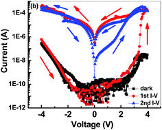
An ultra thin film (∼5 nm) high-k Hafnium oxide dielectric, grown on a doped p-Si(100) substrate by the atomic layer deposition technique has been investigated for resistive and capacitive switching with and without illumination of light. As grown samples illustrate small non-switching leakage current under high applied electric fields and probe frequencies and trap charge assisted counter-clockwise capacitance–voltage behavior. A unique resistance switching was observed under illumination of 15–60 mW light. In the first cycle, the light assisted switching provide a 104:
1 resistance ratio, which diminishes in the next cycle onward, which may be due to irreversible charge injection in the oxide layers. The band offset and band match-up energy diagram for the charge carriers responsible for resistive switching and charge trapping near the interface have been demonstrated under the application of a bias electric field and light.
Ultra thin hafnium oxide (HfO2:
HFO) thin film is one of the most promising material among the high-k dielectrics which has been considered for resistive switching elements due to their high dielectric constant (∼21), low leakage current, high optical band gap (∼5.8 eV), and compatible with silicon.18,19 To utilize very low power consumption and multiple-memory logic states during the read and write process, a novel optical method has been demonstrated in resistive memory devices. Light assisted resistive logic states have been reported for Al2O3 oxide sandwiched between Pd and SiO2/Si with controlled exposure to the top surface of alumina.20 Other binary and ternary oxides have also shown an extra degree of freedom in resistive states under controlled illumination of light, which may be a significant development in the field of information and NVRAM technology.21–23 On the other hand, devices directly integrated on Si is highly sensitive to the illumination of moderate light intensity which partially or permanently changes the band offset alignment and creates photon assisted trap levels near the different interface. To understand the basic physics, band alignment behavior, reproducibility, and device life time, it is due to have methodical investigation on the functional properties of HfO2–SiO2/Si heterostructures under different light ambient condition.
In this report, illumination of light on high-k HFO protective layer with semi transparent top gold metal electrode for Au/HFO/SiO2/Si heterostructure has been studied. Photon assisted charge transport from metal through the insulator layer is facilitated because of the minimal conduction band offset. The illumination of light with certain threshold electric (E)-field on heterostructure has permanently changed the high resistive states of device and the band alignment.
![]() | ||
Fig. 1 (a) show schematic diagram of Au/HFO/SiO2/Si heterostructure, (b) HRTEM image of 600 °C annealed heterostructure with bar scale of 5 nm. |
![]() | ||
Fig. 2 Room temperature grazing incidence X-ray diffraction patterns of Au/HFO/SiO2/Si heterostructure. |
To further check the capacitive performance of MIS capacitors, a typical C–V response of heterostructure was investigated in the frequency range from 1 kHz to 100 kHz at room temperature under dark condition (Fig. 3(a) and (b)). Well defined counterclock wise C–V responses were obtained at various probe frequencies which clearly shows accumulation at negative gate bias voltages and depletion at positive gate bias voltages. Ideally, the high-k dielectric gate should not show any hysteresis in the CV response but there is always trap charges at the interface which develops the hysteresis in C–V curves.27 The observed C–V hysteresis behavior of MIS structure exhibited 1–2 V memory windows in the range of 1–100 kHz, depending on probe frequencies and E-field. The up and down sweeping of C–V curves for 1 kHz probe frequency show a kink near the depletion regions i.e. boundary of accumulation and depletion region suggests high contribution of electronic space charge carriers for low probe frequencies. Each C–V curves show a considerable voltage-axis shift towards positive side due to the presence of interface states. The flat-band voltage shifted toward negative bias as the probe frequency was increased. It is clear from the Fig. 3(b) that the memory window of the C–V hysteresis increases with increase in E-field; however it significantly reduces with increase in probe frequencies. Memory window should provide the different logic states for writing and reading the data bits.28,29 Fig. 3(c) shows the C–V of MIS structure with and without light illumination at 100 kHz and reasonable low E-field stress (∼6 MV cm−1 to avoid breakdown). Interestingly, presence of light populates the charge carriers at p-Si gate and stops the device to reach the inversion states. The depletion region displays two minima like the inverted butterfly loops. These developments are mainly due to the charge carrier injections into the HfO2 ultra thin films. The counter-clockwise C–V hysteresis ruled out the possible polar nature of the HfO2 and trap assisted memory window in C–V curves at high probe frequencies. These are due to trapped charges at the interfaces or injected charges in high-k dielectrics under application of E-stress and illumination of light.
Fig. 4(a) and (b) show the current–voltage (I–V) characteristic of the Au/HFO/SiO2/p-Si heterostructure in dark and under illumination of moderate light energy. Several devices were tested for resistive switching in dark, none of them switched under high E-field (∼8 MV cm−1), and gave extremely low leakage current suitable for next generation logic elements in contrast to earlier report.30 These devices were later illuminated by moderate visible light with power 60 mW which in turn switched the MIS current from high to low resistance states. The average switching E-field and high to low resistance ratio lies in the range of ∼2.8–3.3 MV cm−1 and 104:
1, respectively depending on quality of device. These small variations in switching fields may be due to inhomogeneous distribution of grain boundaries in large device area.12,31 Please note that we have not mentioned the energy density of light source in present investigation, because during illumination of light on devices, large portion of silicon wafer which hold the devices also received light and contribute in transport properties. Interestingly it has been found that once the device switched under light, it never recover the original high resistance, charge injection may permanently changed the band off set and create new impurities charge/trap levels as shown in the band diagram and breakdown mechanism of devices under light (Fig. 6 and 7). These devices were further checked for I–V behavior under illumination of light which display nonlinear I–V curve with high current level and marginal switching on either side of the MIS device. It clearly shows that illumination of light permanently damage the high resistance state of MIS device, the current mechanism can be explained using Poole–Frenkel (PF) or Schottky emission (SE) process.32
A further I–V investigation on the as grown sample with various light illuminations was conducted to check the critical light intensity responsible for permanent damage of high resistance state (Fig. 5). Even small amount of light creates trap levels in the heterostructure and shift the high resistance state towards low resistance state. Utilization of 15 mW light intensity lowered at least one order of resistance without any switching, with further increase in light intensity, MIS structure demonstrates switching but starts form the initial resistance state developed due to illumination of 15 mW intensity. The light intensity was increased from 15 mW to 60 mW to check the switching behavior. The light intensity nearly 30 mW switched the device from high to low resistance state which further re-set to high resistance state during the negative bias E-field which provides a suitable condition for the nonvolatile resistive memory. However the behavior and magnitude of resistive switching varies from device to device and not robust and reproducible in many cases which may be due to the presence and distribution of grain boundaries in that particular device.28 The light intensity ∼45 mW may considered as critical intensity for unrecoverable low resistance state of device and excess charge injection which creates permanent trap levels on either side of the device. It is also clear that with slow and step wise increase in light intensity provide a condition that one cannot observe sharp switching. It suggests that light illumination slowly creates the trap levels in devices which never recovered after removal of light. These devices illustrate nonlinear current response with moderate memory window during forward and reverse (±) E-field switching even after development of permanent trap levels and charge carriers.
![]() | ||
Fig. 5 Illustrates the current–voltage (I–V) curves of Au/HFO/SiO2/Si heterostructure under dark and after illumination of light from 15 to 60 mW. |
Fig. 6 demonstrates the energy level diagram of Au/HFO/SiO2/p-Si hetero-structure. Here Φ is the Au work function 5.1 eV; χ is the semiconductor electron affinity (1.8 eV for HfO2; 0.9 eV for SiO2; and 4.05 eV for Si); Eg is the bandgaps (5.8 eV for HfO2; 8 eV for SiO2; and 1.1 eV for Si); Ev and Ec are the valence and conduction band edges.2,3 In real scenario, the vacuum level can be obtained with slight different position for each material due to charge injection. Two trap levels have been marked in the regions of HfO2 and SiO2 due to charge injections or accumulation after illumination of light. These trap levels are the origin of reduction of barrier height which easily inject electrons and holes in either side of heterostructure under application of external E-field and presence of light. The Schottky barrier for charge injection is relatively higher from Si into SiO2/HfO2 interface; on the other hand trapped charge carriers reduce the electron barrier height near the conduction band. The band match-up demonstrates that the existing MIS structures have a very high band off-set value but it significantly reduces due to development of impurities, trapped charges, and depletion region under illumination of light.
Fig. 7(a) and (b) show the possible change in the barrier heights and the development of charge carriers at interfaces under illumination of white light and the application of positive and negative bias E-field, respectively. Under illumination of light, electrons accumulated the Si–HFO interface and developed the depletion (DL) region (Fig. 7(c)) which creates high resistance states in the device. The devices switched abruptly from high to low resistance state under application of critical applied forward electric field which may be due to the abrupt breakdown the DL regions which set the device at low resistance state. The breakdown of DL region provides the condition to charge carriers for fast and abrupt flow in the external electric circuit and set the device for permanent low resistance state which never recovers under application of negative gate voltage. We elucidate the abrupt change in the current as a modulation of trapped charges across the HFO/Si interface.
To summarize, MIS structure with HFO as high-k dielectric was investigated for capacitive and resistive switching with and without illumination of light. A counter clockwise C–V with 1–2 V memory windows was obtained for MIS structure for high (1–100 kHz) probe frequency in dark that suggests the trap charge assisted capacitive memory developed in the device during the sweeping of gate voltage from negative to positive bias and then again back to negative voltage. Illumination of light has modified the inversion center of the heterostructure and provides an inverted butterfly loop in C–V spectra. Reversible resistive switching was observed below critical light intensity and E-field due to transient trap charges in devices, however the observed phenomena was not robust due the uneven distribution of grain boundaries in the matrix. A sharp but irreversible resistive switching with 104:
1 resistance ratio was observed under illumination of light. It is mainly due to charge injection and permanent creation of trap levels in oxides. A small amount of light may change HFO gated MIS structure from not switchable to switchable resistive states with permanent shift of their high resistance states to several order of low resistance states. This report provides an insight to the researchers and scientists working in area of high-k dielectrics directly integrated with silicon for possible application for resistive switching under moderate and low power light illumination and possible device failure under excess dosage of light illumination.
This journal is © The Royal Society of Chemistry 2015 |