DOI:
10.1039/C5RA03301B
(Paper)
RSC Adv., 2015,
5, 48779-48785
Improved performance of a junctionless tunnel field effect transistor with a Si and SiGe heterostructure for ultra low power applications
Received
22nd February 2015
, Accepted 17th April 2015
First published on 17th April 2015
Abstract
In this paper, we present improved device characteristics of a Junctionless Tunnel Field Effect Transistor (JLTFET) with a Si and SiGe heterostructure. Optimization of the device is done for low power applications. Heterojunction engineering is done to optimize the position of the Si:SiGe junction. Subsequently, band gap engineering is incorporated using variations in doping, gate work function, the mole fraction of SiGe and the dielectric constant. Comparison of the optimized, heterostructured silicon channel using numerical simulations indicates that ION increases from 0.12 to 15 μA μm−1, ION/IOFF increases from 4 × 10⁶ to 3 × 10⁹, and the subthreshold slope decreases from 80 to 43 mV dec−1 for a 22 nm channel with a supply voltage of 0.7 V.
I. Introduction
The presence of two junctions in a metal oxide semiconductor field effect transistor (MOSFET) causes size constraint and so constrains its use in future applications. New perspectives towards Lilienfeld’s first transistor architecture1 resulted in the successful fabrication of a device which does not have any metallurgical junctions thus solving the problem of constraint in the geometry.2–8 Junctionless FETs (JLFETs) could be used in applications such as SRAM, DRAM and flash memory devices.9–11 However, the OFF state current is significant in JLFETs with a less significant improvement in the subthreshold swing, which prevents their use in vast applications. On the contrary, Tunnel Field Effect Transistors (TFETs) are excellent for low power applications with very low leakage and a low subthreshold slope.12,13 However, their low ION prevented further high speed applications. There are various alternatives like germanium channels,14 III–V material channels15 and strained silicon channels. However, the OFF state drain side tunnelling is significant, causing a low current and ON–OFF current ratio in low band gap germanium, III–V materials have dielectric related issues and strained silicon has fabrication concerns.
Recently, Junctionless Tunnel Field Effect Transistors (JLTFETs) have shown good ON state currents and low subthreshold slopes with the combined benefits of JLFETs, which give a high ION, and TFETs, which give a low subthreshold slope.16–20 In this paper, we further improved the characteristics with the use of a Si:SiGe heterojunction for the Low Standby Power technology (LSTP) standards21 of the International Technology Roadmap for Semiconductors (ITRS) with ease of fabrication. High band gap (1.11 eV) Si is placed in the drain side which generates weaker tunnelling in the OFF state, while low band gap (0.67 eV) Ge strengthens band-to-band tunnelling in the ON state. Moreover, a Si and SiGe heterojunction is widely accepted and it has one of the most workable processes in heterostructures. We performed heterojunction engineering to find the optimized position of the heterojunction. Following this, the characteristics are analysed with respect to variations in doping, work function, the mole fraction of Si1−xGex and the dielectric constant. Drastic improvements are found with the optimized heterostructure compared with a Si-JLTFET. Finally, parasitic capacitances and the unity gain frequency of the device are extracted.
II. Device and simulation conditions
A. Device structure
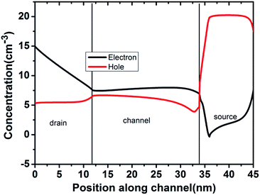
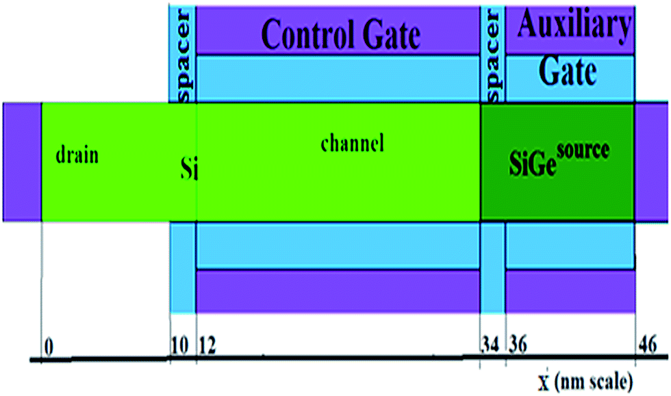
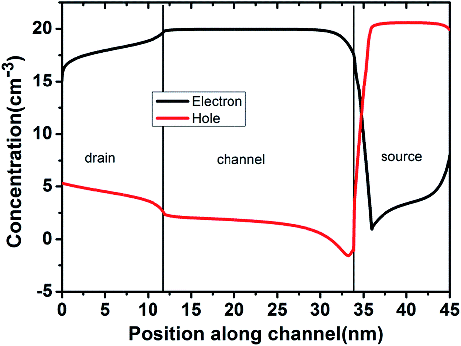
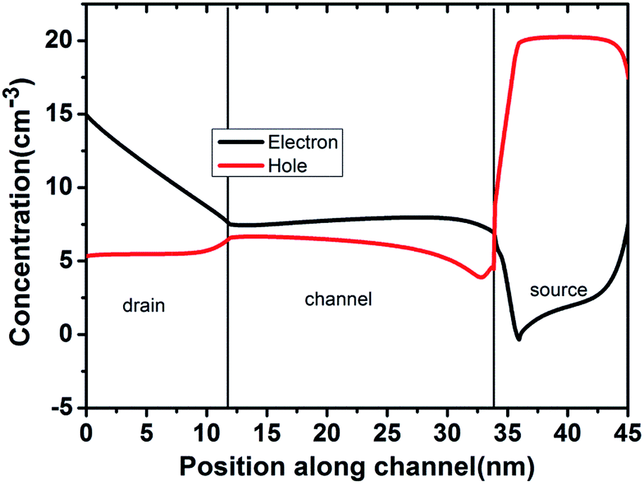
A Hetero-Junctionless Tunnel Field Effect Transistor (H-JLTFET) does not contain any doping junctions as the channel is uniformly n-type doped. Therefore, it is a potential solution for the problem of random dopant fluctuations. The H-JLTFET is structured using a dual n+ polysilicon control gate and a dual p+ polysilicon auxiliary gate at the source side. The work function difference between the control gate and the channel causes an intrinsic region using the charge plasma concept, while the p+ region is caused by the auxiliary gate and the channel work function difference, resulting in the creation of p+:i:n+ regions. H-JLTFETs work on band-to-band tunnelling to implement a higher ION and  device with a lower subthreshold slope. Steeper energy bands have to be created with propinquity of bands in the tunnelling region with higher band overlap. Use of a heterojunction of Si at the drain side and SiGe at the source side satisfies the above conditions. The structure of the Si:SiGe H-JLTFET is shown in Fig. 1 with a heterojunction position, xj, at 34 nm. The electron and hole concentration profile of the Si:SiGe H-JLTFET is depicted in Fig. 2 as a function of distance along the x-direction in the ON state. The intrinsic region band energy shifts downward by applying sufficient positive gate voltage. This leads to p+:n+:n+ regions from the p+:i:n+ regions and hence makes sufficient conditions for tunnelling. The device works on a flat band when the device is in the ON state causing almost zero resistance, while the device is depleted of carriers in the OFF state, giving no current. The OFF state carrier concentration profile of the proposed structure is shown in Fig. 3. Process attempts at the Si:Si1−xGex interface resulted in significant progress and indicated it as the most suited potential candidate in heteroengineering.22–24 A Si1−xGex source layer could be smoothly fabricated for x = 0.15 to x = 0.30. Higher mole fractions of Ge may lead to defect formation at the channel interface. Also, vertical heterostructures could be a viable solution for the fabrication of this device as vertical structures have resulted in the successful fabrication of many devices.23–29 We have used HfO2 as a gate dielectric. It could be fabricated using atomic layer deposition (ALD), and through ALD, surface oxides are largely eliminated.
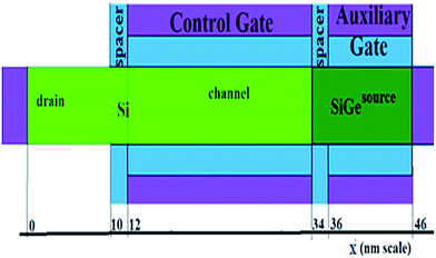 |
| | Fig. 1 The structure of a Si:SiGe Hetero-Junctionless Tunnel Field Effect Transistor (H-JLTFET) with a heterojunction position, xj, at 34 nm. | |
 |
| | Fig. 2 The electron and hole concentration profile of the Si:SiGe H-JLTFET as a function of distance along the x-direction in the ON state (VDS = 0.7 V, VGS = 0.7 V) with preset parameters. | |
 |
| | Fig. 3 The electron and hole concentration profile of the Si:SiGe H-JLTFET as a function of distance along the x-direction in the OFF state (VDS = 0.7 V, VGS = 0 V) with preset parameters. | |
B. Simulation setup
Simulations are done in a SILVACO ATLAS 2D Device Simulator, using the band-to-band tunnelling (BBT)30 model for including the effect of tunnelling. In the BBT model, we used non-local models which are independent of an electric field at individual mesh points and the tunnelling current depends on the band structure along the cross section taken through the device.31 As the channel is heavily doped, the Band Gap Narrowing (BGN) model has been added.31 Other models include Shockley–Read–Hall (SRH) to model traps or defects,31,32 and Schenk’s Trap Assisted Tunnelling (TAT) model to account for electron tunnelling through the band gap via trap states32. The Quantum Confinement (QC) model for the interface trap effect and quantum confinement effect31,33 is also considered. Heavy doping and a thin oxide are enough for the creation of a potential well in the channel during inversion and therefore quantum confinement must be incorporated. The preset parameters used for device simulation of the H-JLTFET as in Fig. 1 are tabulated in Table 1.
Table 1 Preset parameters for device simulation of the H-JLTFET
| Parameter |
Value |
| Source/channel/drain doping (ND) (uniformly doped) |
1 × 1019 cm−3 (unless otherwise specified) |
| Effective oxide thickness (TOX) |
2 nm |
| Control gate work function (ΦG) |
4.2 eV (unless otherwise specified) |
| Auxiliary gate work function (ΦS) |
5.3 eV |
| Gate length (Lg) |
22 nm |
| Heterojunction position (xj) |
34 nm (unless otherwise specified) |
| Channel thickness (Tch) |
5 nm |
| Supply voltage (VDD) |
0.7 V |
| Permittivity of dielectric material (εd) |
25 (unless otherwise specified) |
| Spacers (low-k) |
3.9 |
| Mole fraction of Si1−xGex (x) |
0.5 (unless otherwise specified) |
III. Optimization of the H-JLTFET
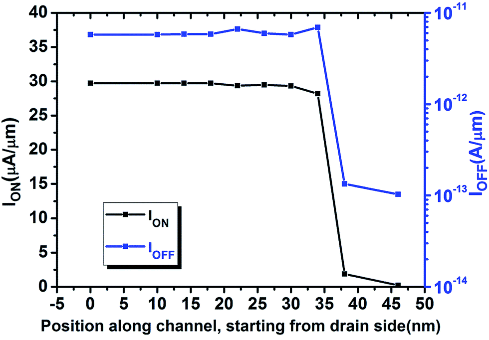
Fig. 4 plots the ION and IOFF with respect to the heterojunction position, xj. As the supply voltage is very low, the ON and some part of the OFF state tunnelling occurs in the source region, contrary to TFETs where the OFF state tunnelling mainly occurs in the drain side. Therefore, variation in xj across the channel depicts a smaller variation in the ON and OFF currents until the source region is covered by SiGe. Similarly, the values of  and subthreshold slope are finer with the presence of SiGe at the source side, whereas they drop drastically in the presence of a larger band gap silicon material at the source side. This is illustrated in Fig. 5. Two structures can be preferred from the view of fabrication: first, Si:SiGe with a heterojunction position, xj, at 34 nm (i.e. in situ SiGe source). There is no interaction of SiGe with the gate dielectric and the lesser region contains germanium which brings costs down. The second is a homogeneous Si1−xGex JLTFET structure which does not have any heterojunctions. It works with the problem of gate insulator fabrication. Moreover, the number of steps and the power budget in the process could be reduced because of the absence of heterojunctions. However, a Si1−xGex H-JLTFET exhibits less improvement in device performance when the structural parameters are optimized. Furthermore, heterostructured Si:SiGe has higher suppressed tunnelling between the drain and channel than a homogeneous SiGe device which brings very low leakage.
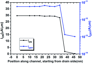 |
| | Fig. 4 ON and OFF state currents with respect to the position of the heterojunction, xj, of a Si:SiGe H-JLTFET with VDD = 0.7 V, ΦG = 4.2 eV, εd = 25, x = 0.5 and ND = 1019 cm−3. | |
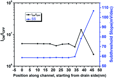 |
| | Fig. 5  and subthreshold slope with respect to the position of the heterojunction, xj, of a Si:SiGe H-JLTFET with VDD = 0.7 V, ΦG = 4.2 eV, εd = 25, x = 0.5 and ND = 1019 cm−3. and subthreshold slope with respect to the position of the heterojunction, xj, of a Si:SiGe H-JLTFET with VDD = 0.7 V, ΦG = 4.2 eV, εd = 25, x = 0.5 and ND = 1019 cm−3. | |
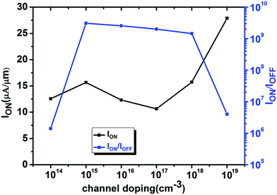
Variation in the concentration of dopant causes a change in the work function of a semiconductor and hence the energy band diagram of the device. The highest  is obtained at a channel doping, ND, of 1015 cm−3 as shown in Fig. 6. Interestingly, with a low process budget and low temperature process, the intrinsic channel results in the highest ON and OFF state current ratio. However, at a very high doping of 1019 cm−3, energy band overlap increases causing a higher ION and IOFF and subsequently, a lower
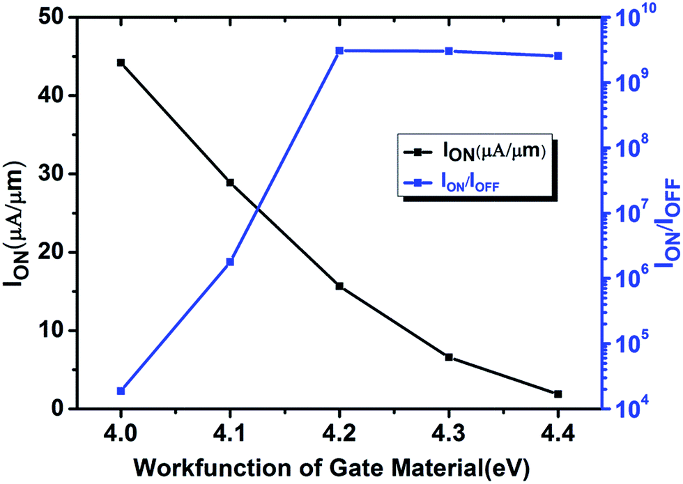
  . Reduction in the work function of the gate brings more electrons near the surface. This results in more band overlap bringing a higher ION and IOFF, and a gate work function, ΦG, of 4.2 eV yields the highest
  . The ON current and
  with respect to the work function of the control gate material is shown in Fig. 7.
 |
| | Fig. 6 ON current and ON and OFF current ratio versus channel doping with VDD = 0.7 V, ΦG = 4.2 eV, εd = 25, xj = 34 nm and x = 0.5 for a Si:SiGe H-JLTFET. | |
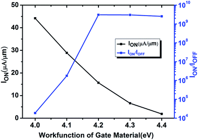 |
| | Fig. 7 ON current and ON and OFF current ratio versus work function of the control gate material with VDD = 0.7 V, ND = 1015 cm−3, εd = 25, xj = 34 nm and x = 0.5 for a Si:SiGe H-JLTFET. | |
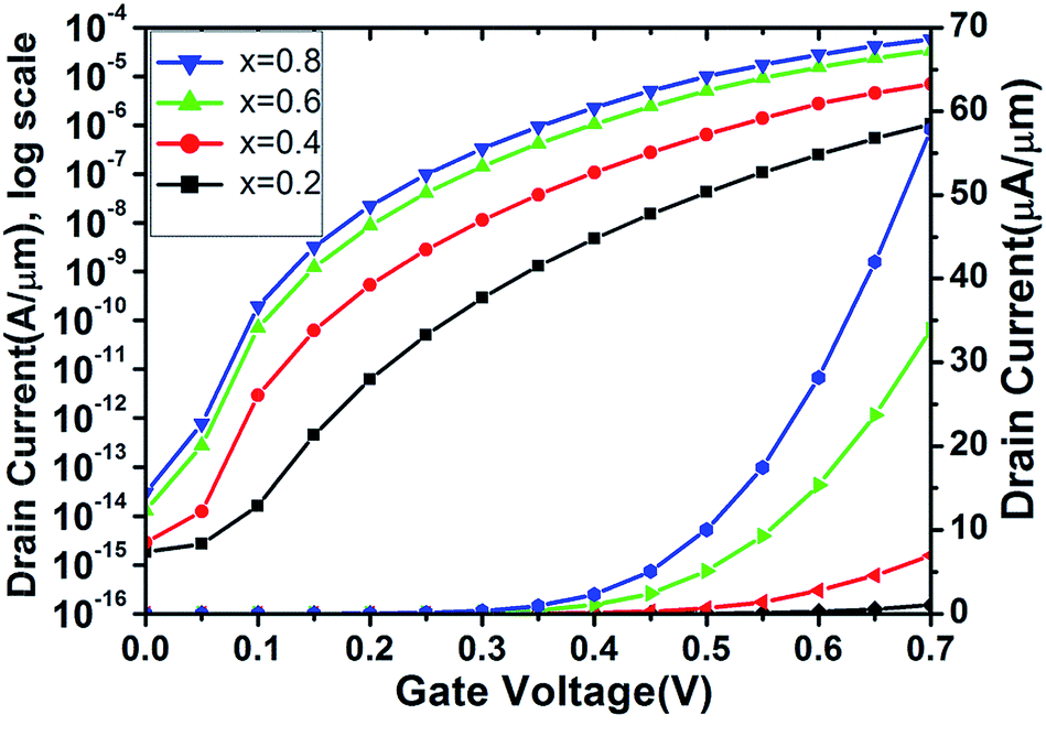
One can increase current through increasing the overlap region of the bands. This can be done through a higher mole fraction, x, of germanium in the source side of Si1−xGex which produces a lower band gap near the source side and gives a higher drain current as shown in Fig. 8. However, fabrication of a transistor with a mole fraction, x, higher than 0.5 carries the issue of strain.
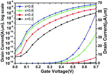 |
| | Fig. 8 Drain current versus gate voltage for a varying mole fraction, x, of Si1−xGex with VDD = 0.7 V, ND = 1015 cm−3, ΦG = 4.2 eV, εd = 25 and xj = 34 nm for a Si:SiGe H-JLTFET. | |
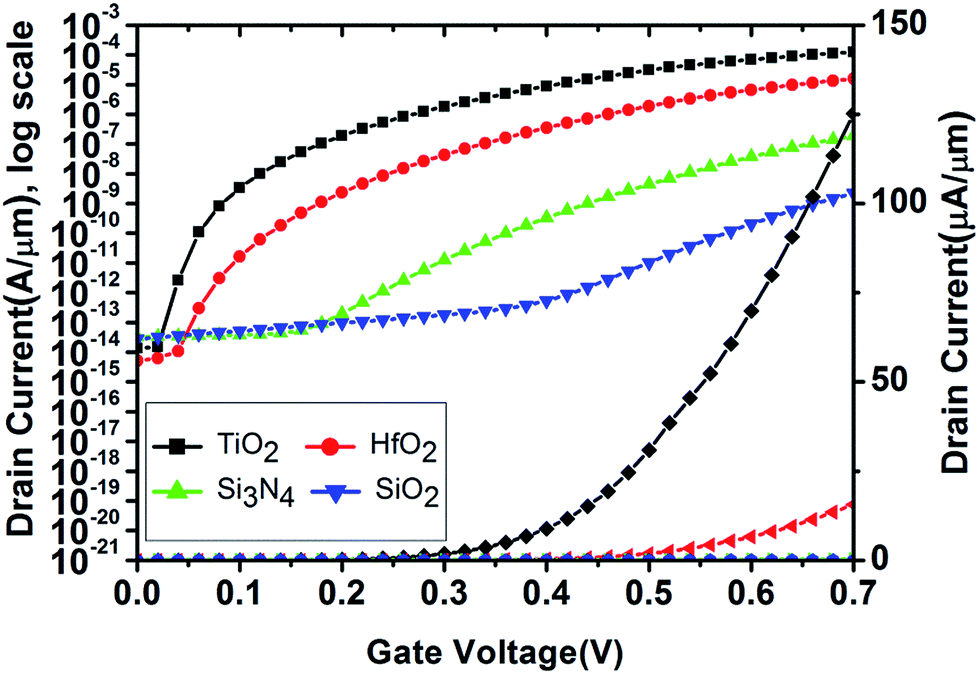
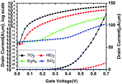
Substantial research has been done on dielectric materials for optimizing current.34,35 Drain current is measured for four dielectrics, namely SiO2(3.9), Si3N4(7), HfO2(25) and TiO2(80),36,37 as shown in Fig. 9. Increasing permittivity increases the ON state current and decreases the OFF state current as gate control proliferates because of the permittivity of the dielectric. Consequently,  rises along with a significant improvement in the subthreshold slope. ION and
  for TiO2 are 125 μA μm−1 and 9 × 10⁹ respectively. There is a more than 5 × 10⁴ times improvement in ION for TiO2 with respect to SiO2.
 |
| | Fig. 9 Drain current versus gate voltage for varying permittivity with VDD = 0.7 V, ND = 1015 cm−3, ΦG = 4.2 eV, xj = 34 nm and x = 0.5 for a Si:SiGe H-JLTFET. | |
IV. Results and discussion
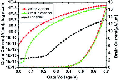
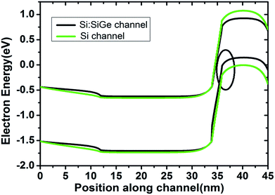
Through variations of various device parameters, we found that ΦG = 4.2 eV, εd = 25, x = 0.5, xj = 34 nm and ND = 1015 cm−3 resulted in an optimized device performance. However, a value of x above 0.3 can create a feasibility constraint of the process. Therefore, until x = 0.3, we can get performance improvement along with an insignificant improvement in cost as we have removed doping junctions from the structure. The transfer characteristic of the proposed device is compared with that of a Si JLTFET and Si0.5Ge0.5 JLTFET in Fig. 10. Clearly, the Si:SiGe channel has a much better transfer characteristic than Si and SiGe channels for low power applications. The Si JLTFET has lower currents than the SiGe JLTFET due to the reduced band gap of Si0.5Ge0.5. The ON state energy band diagram indicates that there is reduced tunnelling near the source for the silicon channel in comparison to the Si:SiGe channel, and thus a lower drain current follows. This is elaborated in Fig. 11. Comparison of the device characteristics is done in Table 2. It is evident from the table that heterostructured and high-k dielectric materials improve the JLTFET performance drastically. The Si:Si0.5Ge0.5 H-JLTFET with TiO2 as a gate dielectric provides the best results with a subthreshold slope as low as 23 mV dec−1. The subthreshold slope is calculated with the following formula:| |
 | (1) |
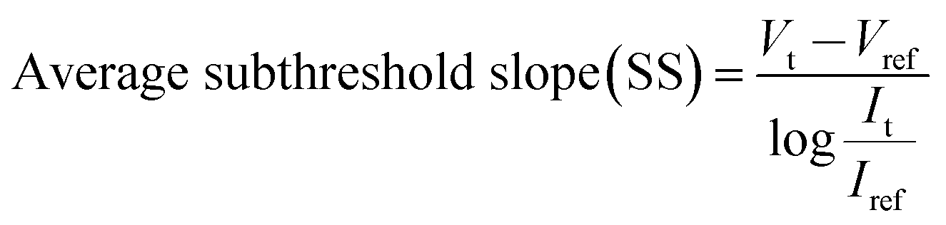
where It is taken as 10−7 A μm−1, Vt is the voltage at the point where the current crosses 10−7 A μm−1, and Vref is the voltage at the reference point. Clearly, from Table 2 we can conclude that the H-JLTFET surpasses the benchmark of ITRS’ LSTP for 22 nm technology and supplies a voltage of 0.7 V.
 |
| | Fig. 10 Variation of drain current with gate voltage at VDD = 0.7 V, ND = 1015 cm−3, ΦG = 4.2 eV, xj = 34 nm, x = 0.5 and εd = 25 for the SiGe JLTFET, Si:SiGe H-JLTFET and Si JLTFET. | |
 |
| | Fig. 11 ON state energy band diagram showing reduced tunnelling near the source for the Si JLTFET in comparison to the Si:SiGe H-JLTFET at VDD = 0.7 V, ND = 1015 cm−3, ΦG = 4.2 eV, xj = 34 nm, x = 0.5 and εd = 25. | |
Table 2 Characteristics of JLTFETS and H-JLTFETS
| |
Si JLTFET (HfO2, εd = 25) |
SiGe JLTFET (HfO2, εd = 25) |
Si:Si0.5Ge0.5 H-JLTFET (HfO2, εd = 25) |
Si:Si0.5Ge0.5 H-JLTFET (TiO2, εd = 80) |
| ION (μA μm−1) |
0.12 |
29.72 |
15.66 |
125.27 |
| IOFF (A μm−1) |
2.6 × 10⁻¹⁴ |
5.8 × 10⁻¹² |
5.1 × 10⁻¹⁵ |
1.35 × 10⁻¹⁴ |
 |
4 × 10⁶ |
5 × 10⁶ |
3 × 10⁹ |
9 × 10⁹ |
| SS (avg.) (mV dec−1) |
80 |
59 |
43 |
23 |
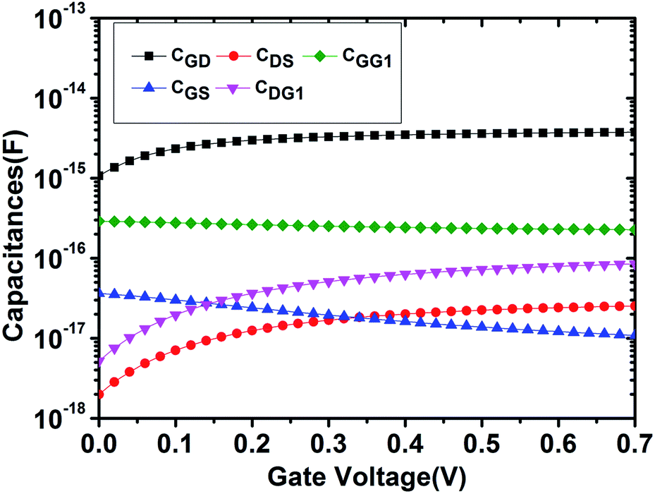
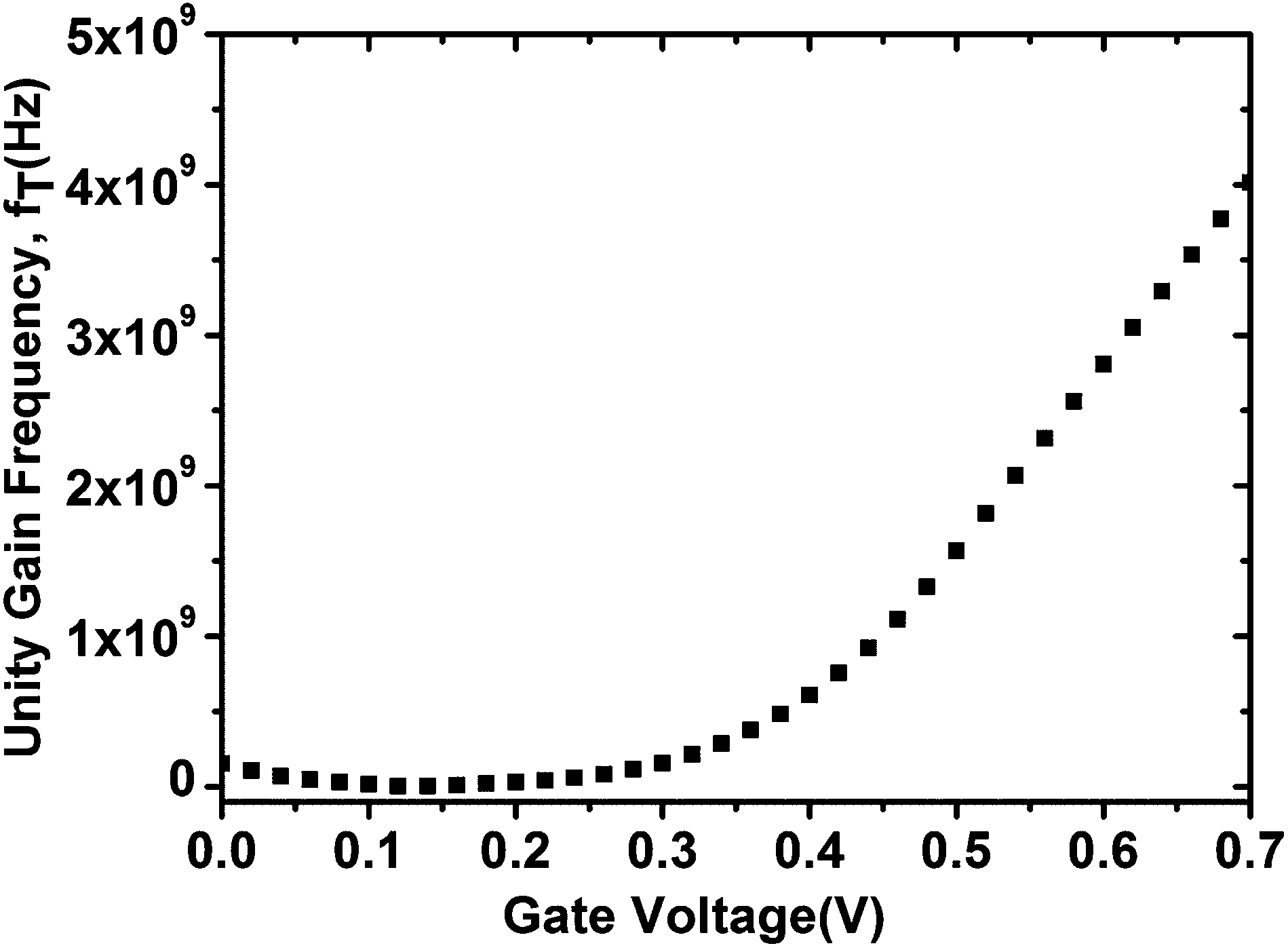
Capacitance between the gate and source (CGS), gate and drain (CGD), gate and auxiliary gate (CGG1), drain and source (CDS) and drain and auxiliary gate (CDG1) as a function of gate voltage at a drain voltage of 0.7 V are extracted and plotted in Fig. 12. Here, ‘G1’ represents the auxiliary gate. All the capacitances are extracted for the small signal of 0.01 V and a frequency of 1 MHz. The device approaches a linear region with VGS; thus CGD grows while CGS decreases. Due to the carrier concentration profile as in Fig. 2, CGD is higher than CGS. Computation results in a maximum unity gain frequency, fT, of 4 × 10⁹ at the supply voltage. Unity gain frequency, fT, is compiled as a function of the gate voltage at VDS = 0.7 V in Fig. 13.
 |
| | Fig. 12 Variation of capacitances, CGD, CDS, CGS, CDG1 and CGG1, with gate voltage at VDS = 0.7 V for the Si:SiGe H-JLTFET with ac freq. = 1 MHz, small signal = 0.01 V, ND = 1015 cm−3, ΦG = 4.2 eV, xj = 34 nm, x = 0.5 and εd = 25. | |
 |
| | Fig. 13 Unity gain frequency, fT, as a function of the gate voltage at VDS = 0.7 V for the Si:SiGe H-JLTFET with ac freq. = 1 MHz, small signal = 0.01 V, ND = 1015 cm−3, ΦG = 4.2 eV, xj = 34 nm, x = 0.5 and εd = 25. | |
V. Conclusion
We can conclude that the H-JLTFET exhibits tremendous characteristics for the 22 nm Low Standby Power technology (LSTP) standards of the International Technology Roadmap for Semiconductors (ITRS) with ease of fabrication, as channel doping and the dielectric oxide thickness were kept at 1015 and 2 nm respectively. For a 22 nm channel, a very low leakage current of ∼10−15 A μm−1 and an ON and OFF state current ratio of the order of 109 at a VDD of 0.7 V and a dielectric constant of 25 are achieved. Furthermore, the performance improves with a very high-k dielectric, and TiO2 and the H-JLTFET easily surpass all standards of the LSTP. Comparing this device data with recently developed structures, the H-JLTFET is far ahead in terms of performance. Because of these exceptional characteristics for very small geometries at a low voltage, the H-JLTFET is a promising solution for low power applications.
References
- J. E. Lilienfeld, Method and apparatus for controlling electric current, U.S. Pat. 1745175, 1930.
- J.-P. Colinge, C.-W. Lee, A. Afzalian, N. D. Akhavan, R. Yan, I. Ferain, P. Razavi, B. O’Neill, A. Blake, M. White, A.-M. Kelleher, B. McCarthy and R. Murphy, Nanowire transistors without junctions, Nat. Nanotechnol., 2010, 5(3), 225–229 CrossRef CAS PubMed.
- C.-W. Lee, A. Afzalian, N. D. Akhavan, R. Yan, I. Ferain and J.-P. Colinge, Junctionless multigate field-effect transistor, Appl. Phys. Lett., 2009, 94(5), 053511–053512 CrossRef PubMed.
- B. Soree, W. Magnus and G. Pourtois, Analytical and self-consistent quantum mechanical model for a surrounding gate MOS nanowire operated in JFET mode, J. Comput. Electron., 2010, 7(3), 380–383 CrossRef PubMed.
- A. Kranti, C.-W. Lee, I. Ferain, R. Yu, N. D. Akhavan, P. Razavi and J. Colinge, Junctionless nanowire transistor: Properties and design guidelines, Proc. 34th IEEE Eur. Solid-State Device Res. Conf., 2010, pp. 357–360 Search PubMed.
- S. Gundapaneni, S. Ganguly and A. Kottantharayil, Bulk planar junctionless transistor (BPJLT): An attractive device alternative for scaling, IEEE Electron Device Lett., 2011, 32(3), 261–263 CrossRef CAS.
- S. Gundapaneni, S. Ganguly and A. Kottantharayil, Enhanced electrostatic integrity of short channel junctionless transistor with high-κ spacers, IEEE Electron Device Lett., 2011, 32(10), 1325–1327 CrossRef CAS.
- C.-W. Lee, I. Ferain, A. Afzalian, R. Yan, N. D. Akhavan, P. Razavi and J.-P. Collinge, Performance estimation of junctionless multigate transistors, Solid-State Electron., 2010, 54(2), 97–103 CrossRef CAS PubMed.
- S.-J. Choi, D.-I. Moon, S. Kim, J.-H. Ahn, J.-S. Lee, J.-Y. Kim and Y.-K. Choi, Nonvolatile memory by all-around-gate junctionless transistor composed of silicon nanowire on bulk substrate, IEEE Electron Device Lett., 2011, 32(5), 602–604 CrossRef CAS.
- C.-W. Lee, R. Yan, I. Ferain, A. Kranti, N. Akhvan, P. Razavi, R. Yu and J. Colinge, Nanowire zero-capacitor DRAM transistors with and without junctions, Proc. 10th IEEE-NANO, 2010, pp. 242–245 Search PubMed.
- A. Kranti, C. Lee, I. Ferain, R. Yan, N. Akhavan, P. Razavi, R. Yu, G. A. Armstrong and J. Colinge, Junctionless 6T SRAM cell, IET Electronics Letters, 2010, 46(22), 1491–1493 CrossRef.
- K. Boucart and A. M. Ionescu, Double gate tunnel FET high K gate dielectric, IEEE Trans. Electron Devices, 2007, 54(7), 1725–1733 CrossRef CAS.
- M. T. Bjork, J. Knoch, H. Schmid, H. Riel and W. Riess, Silicon nanowire tunneling field-effect transistors, Appl. Phys. Lett., 2008, 92(19), 193504 CrossRef PubMed.
- D. Kazazis, P. Jannaty, A. Zaslavsky, C. Le Royer, C. Tabone, L. Clavelier and S. Cristolovean, Tunneling field-effect transistor with epitaxial junction in thin germanium-on-insulator, Appl. Phys. Lett., 2009, 94, 263508 CrossRef PubMed.
- K. Ganapathi, Y. Yoon and S. Salahuddin, Analysis of InAs vertical and lateral band-to-band tunneling transistors: Leveraging vertical tunneling for improved performance, Appl. Phys. Lett., 2010, 97, 033504 CrossRef PubMed.
- P. K. Asthana, B. Ghosh, S. B. M. Rahi and Y. Goswami, Optimal design for a high performance H-JLTFET using HfO2 as a gate dielectric for ultra low power applications, RSC Adv., 2014, 4, 22803–22807 RSC.
- B. Ghosh and M. W. Akram, Junctionless Tunnel Field Effect Transistor, IEEE Electron Device Lett., 2013, 34(5), 584–586 CrossRef CAS.
- B. Ghosh, P. Bal and P. Mondal, A junctionless tunnel field effect transistor with low subthreshold slope, J. Comput. Electron., 2013, 12(3), 428–436 CrossRef CAS.
- P. Bal, M. W. Akram, P. Mondal and B. Ghosh, Performance estimation of sub-30 nm junctionless tunnel FET (JLTFET), J. Comput. Electron., 2013, 12(4), 782–789 CrossRef.
- P. Bal, B. Ghosh, P. Mondal, M. W. Akram and B. Mukund Tripathi, Dual material gate junctionless tunnel field effect transistor, J. Comput. Electron., 2014, 13(1), 230–234 CrossRef CAS.
- C. Calvin Hu, Modern Semiconductor Devices for Integrated Circuits, Pearson India, 1st edn, 2010, pp. 279–280 Search PubMed.
- U. Konig, et al., N- and p-type Si–SiGe hetero FETs, IEEE Int. Symp. on High Perf. Electron. Dev. for Microwave and Optoelectronic Appl., 2000, vol. 8, pp. 1–7 Search PubMed.
- M. Schmidt, et al., Si/SiGe Hetero-Structure Tunneling Field Effect Transistors with In Situ Doped SiGe Source, Int. Conf. on ULIS, 2012, vol. 13, pp. 191–194 Search PubMed.
- C. Wang and S. Y. Chou, Self-aligned fabrication of 10 nm wide asymmetric trenches for Si/SiGe heterojunction tunneling field effect transistors using nanoimprint lithography, shadow evaporation, and etching, J. Vac. Sci. Technol., B: Microelectron. Nanometer Struct.–Process., Meas., Phenom., 2009, 27(6), 2790–2794 CrossRef CAS.
- A. M. Ionescu and H. Riel, Tunnel field-effect transistors as energy-efficient electronic switches, Nature, 2011, 479, 329–337 CrossRef CAS PubMed.
- D. Sacchetio, M. Haykel Ben-Jamaal, G. De Michelil and Y. Leblebici, Fabrication and Characterization of Vertically Stacked Gate-AIl-Around Si Nanowire FET Arrays, Proc. of the 39th European Solid-State Dev. Res. Conf. (ESSDERC), 2009 Search PubMed.
- N. Shen, T. T. Le, H. Y. Yu, Z. X. Chen, K. T. Win, N. Singh, G. Q. Lo and D.-L. Kwong, Fabrication and Characterization of Poly-Si Vertical Nanowire Thin Film Transistor, World Acad. of Sci, Eng. and Tech, 2011, vol. 57 Search PubMed.
- T. T. Le, H. Y. Yu, Y. Sun, N. Singh, X. Zhou, N. Shen, G. Q. Lo and D. L. Kwong, High-Performance Poly-Si Vertical Nanowire Thin-Film Transistor and the Inverter Demonstration, IEEE Electron Device Lett., 2011, 32(6), 1102–1106 CrossRef.
- R. Yang, et al., Two Dimensional Device Simulation and Fabrication of Mesa SOI Vertical Dual Carrier Field Effect Transistor with Effective Channel Length of 30nm for Switching ASIC and SOC, 6th ASICON, 2005, vol. 2, pp. 1102–1106 Search PubMed.
- http://www.steeper-project.org/resources/Dissemination/Workshops/Sispad2010_Workshop/talk8_Palestri.pdf, accessed on 19 June, 2013.
- http://www.silvaco.com, accessed on 27 July, 2013.
- A. Schenk, A model for the field and temperature dependence of SRH lifetimes in Silicon, Solid-State Electron., 1992, 35(11), 1585–1596 CrossRef CAS.
- W. Hansch, T. Vogelsang, R. Kirchner and M. Orlowski, Carrier Transport Near the Si/SiO2 Interface of a MOSFET, Solid-State Electron., 1989, 32(10), 839–849 CrossRef.
- K. Boucart, Simulation of Double-Gate Silicon Tunnel FETs with a High-k Gate Dielectric, ecole polytechnique federale de Lausanne, Switz., 2010 DOI:10.5075/epfl-thesis-4729.
- C. Anghel, P. Chilagani, A. Amara and A. Vladimirescu, Tunnel field effect transistor with increased ON current, low-k spacer and high-k dielectric, Appl. Phys. Lett., 2010, 96, 122104, DOI:10.1063/1.3367880.
- J. Robertson, High dielectric constant oxide, Eur. Phys. J.: Appl. Phys., 2010, 3, 265–291 Search PubMed.
- M. Seo, S. Keun Kim, J. Hwan Han and C. S. Hwang, Permittivity Enhanced Atomic Layer Deposited HfO2 Thin Films Manipulated by a Rutile TiO2 Interlayer, Chem. Mater., 2010, 22(15), 4419–4425 CrossRef CAS.
|
| This journal is © The Royal Society of Chemistry 2015 |
Click here to see how this site uses Cookies. View our privacy policy here. 
 device with a lower subthreshold slope. Steeper energy bands have to be created with propinquity of bands in the tunnelling region with higher band overlap. Use of a heterojunction of Si at the drain side and SiGe at the source side satisfies the above conditions. The structure of the Si:SiGe H-JLTFET is shown in Fig. 1 with a heterojunction position, xj, at 34 nm. The electron and hole concentration profile of the Si:SiGe H-JLTFET is depicted in Fig. 2 as a function of distance along the x-direction in the ON state. The intrinsic region band energy shifts downward by applying sufficient positive gate voltage. This leads to p+:n+:n+ regions from the p+:i:n+ regions and hence makes sufficient conditions for tunnelling. The device works on a flat band when the device is in the ON state causing almost zero resistance, while the device is depleted of carriers in the OFF state, giving no current. The OFF state carrier concentration profile of the proposed structure is shown in Fig. 3. Process attempts at the Si:Si1−xGex interface resulted in significant progress and indicated it as the most suited potential candidate in heteroengineering.22–24 A Si1−xGex source layer could be smoothly fabricated for x = 0.15 to x = 0.30. Higher mole fractions of Ge may lead to defect formation at the channel interface. Also, vertical heterostructures could be a viable solution for the fabrication of this device as vertical structures have resulted in the successful fabrication of many devices.23–29 We have used HfO2 as a gate dielectric. It could be fabricated using atomic layer deposition (ALD), and through ALD, surface oxides are largely eliminated.
 and subthreshold slope are finer with the presence of SiGe at the source side, whereas they drop drastically in the presence of a larger band gap silicon material at the source side. This is illustrated in Fig. 5. Two structures can be preferred from the view of fabrication: first, Si:SiGe with a heterojunction position, xj, at 34 nm (i.e. in situ SiGe source). There is no interaction of SiGe with the gate dielectric and the lesser region contains germanium which brings costs down. The second is a homogeneous Si1−xGex JLTFET structure which does not have any heterojunctions. It works with the problem of gate insulator fabrication. Moreover, the number of steps and the power budget in the process could be reduced because of the absence of heterojunctions. However, a Si1−xGex H-JLTFET exhibits less improvement in device performance when the structural parameters are optimized. Furthermore, heterostructured Si:SiGe has higher suppressed tunnelling between the drain and channel than a homogeneous SiGe device which brings very low leakage.
 and subthreshold slope with respect to the position of the heterojunction, xj, of a Si:SiGe H-JLTFET with VDD = 0.7 V, ΦG = 4.2 eV, εd = 25, x = 0.5 and ND = 1019 cm−3.
 is obtained at a channel doping, ND, of 1015 cm−3 as shown in Fig. 6. Interestingly, with a low process budget and low temperature process, the intrinsic channel results in the highest ON and OFF state current ratio. However, at a very high doping of 1019 cm−3, energy band overlap increases causing a higher ION and IOFF and subsequently, a lower
  . Reduction in the work function of the gate brings more electrons near the surface. This results in more band overlap bringing a higher ION and IOFF, and a gate work function, ΦG, of 4.2 eV yields the highest
  . The ON current and
  with respect to the work function of the control gate material is shown in Fig. 7.
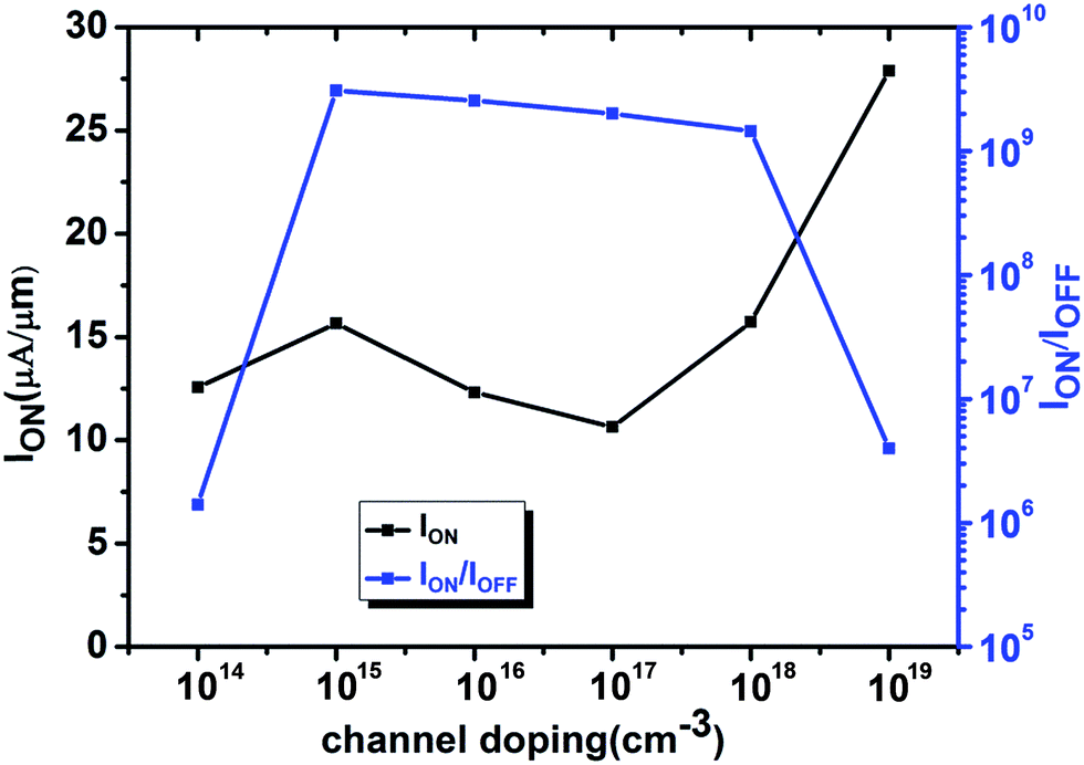
 rises along with a significant improvement in the subthreshold slope. ION and
  for TiO2 are 125 μA μm−1 and 9 × 10⁹ respectively. There is a more than 5 × 10⁴ times improvement in ION for TiO2 with respect to SiO2.