Yesul Jeonga,
Christopher Pearsona,
Hyun-Gwan Kimb,
Man-Young Parkb,
Hongdoo Kimc,
Lee-Mi Dod and
Michael C. Petty*a
aSchool of Engineering and Computing Sciences and Centre for Molecular and Nanoscale Electronics, Durham University, South Road, Durham DH1 3LE, UK. E-mail: m.c.petty@durham.ac.uk
bResearch Center for Nano-Materials, DNF Co. Ltd., Daejeon 306-802, Korea
cDepartment of Advanced Materials Engineering for Information and Electronics, Kyung Hee University, Yongin 446-701, Korea
dIT Convergence Technology Research Laboratory, Electronics and Telecommunications Research Institute, Daejeon, Korea
First published on 15th April 2015
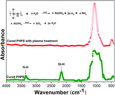
We report on the low-temperature formation (180 °C) of a SiO2 dielectric layer from solution-processed perhydropolysilazane. A bottom-gate zinc oxide thin-film transistor has subsequently been fabricated that possesses a carrier mobility of 3 cm2 V s−1, an on/off ratio of 107 and minimal hysteresis in its transfer and output characteristics.
Studies of compatible gate insulators to use with ZnO TFTs are now increasing. Organic materials, e.g. PS-b-PMMA, inorganic compounds, e.g. Al2O3, Y2O3, HfO, and hybrid structures, e.g. LaZrOX/SiO2, PVP/Al2O3 PMMA/SiO2, CNO-PMMA, PMSQ are all attractive candidates for solution-processed gate dielectrics.1–6 However, it should be noted that there are relatively few studies reporting ZnO TFTs using solution processing for fabricating both the semiconductor and gate insulator layers.7–10 There remain many issues to be addressed. For example, Jung et al.7 noted that films of organic gate insulators including poly(4-vinylphenol), poly-methacrylate, polyimide and polyvinyl alcohol can be solution processed at low temperature. However, the thin films can easily be damaged by ammonia in the ZnO solution. In addition, solution-processed ZnO TFTs with organic gate insulators can possess relatively low field-effect mobilities.8 Ko et al.9 examined solution-processed ZnO transistors with a HfLaOX gate insulator. This material, annealed at 500 °C, exhibited a low leakage current and a high dielectric constant; a TFT with good electrical properties was subsequently fabricated (carrier mobility of 1.6 cm2 V−1 s−1). However, the processing temperature of 500 °C is unsuitable for flexible display substrates.
Organosiloxane-based organic–inorganic hybrid gate insulators have also been studied.7 Although both ZnO and the gate insulator were formed by spin coating and a relatively low annealing temperature of 230 °C was employed, the devices possessed a field effect mobility of 0.32 cm2 V−1 s−1, a threshold voltage of 0.89 V and on/off ratio of ∼105.
Silicon dioxide (SiO2), deposited by plasma-enhanced CVD, has been extensively used as a gate insulator for ZnO TFTs as the devices generally show excellent electrical performance, with high mobility, on/off ratio and stability. Commercial production of ZnO TFTs has already adopted SiO2 as the gate insulator. A disadvantage, however, is that the processing takes place in a high vacuum system at an elevated temperature. A notable recent achievement by Wu et al.5,6 is the low-temperature solution processing of printable indium–gallium–zinc oxide TFTs at 150 °C. Relatively high mobilities (>0.8 cm2 V s−1) were obtained, although an additional passivation layer was required to achieve high on/off ratios and low leakage currents.
Perhydropolysilazane (PHPS) offers an attractive, low-temperature route to the preparation of SiO2 thin films. This precursor polymer is composed of a network of Si–N, Si–H and N–H chemical groups; solution processing can be conveniently used to convert the material into either dense Si3N4 or SiO2 films, depending on the precise processing conditions. For example, Matsuo et al.11 have developed SiO2 films having a density of 2.1–2.2 g cm−3, a refractive index of 1.45–1.46 and a dielectric constant of 4.2 using PHPS deposited onto a Si substrate. These parameters are comparable to values for vacuum-processed SiO2 prepared at a high reaction temperature (density of 2.0–2.3 g cm−3, refractive index of 1.46 and dielectric constant of 3.9). In addition, this study demonstrated that PHPS can be transformed into SiO2 by heat treatment at 450 °C, but the addition of a catalyst to the PHPS can reduce the processing temperature (300–350 °C). Much research is now being undertaken to optimise the conversion method in order to lower further the processing temperature.12–16 For example, Bauer et al.12 introduced moisture during the heat treatment, which had a significant effect on accelerating the reaction, although it still proved difficult to form a fully converted SiO2 film at temperatures lower than 150 °C.
In this study, a solution-processed SiO2 gate insulator is prepared from PHPS using spin coating and a low curing temperature of 180 °C. To complete the conversion to SiO2, an oxygen plasma treatment is used after the curing process. The film properties are examined using atomic force microscopy (AFM), Fourier transform infrared (FTIR) spectroscopy and electrical conductivity measurements. We demonstrate that the plasma-treated SiO2 gate insulator can be used in a bottom-gate TFT architecture to achieve solution-processed ZnO TFTs with excellent electrical performance.
The conversion of PHPS in a high humidity environment is depicted in Fig. 1(a). Ideally, hydrolysis and polycondensation are the main routes to form SiO2 from PHPS.12 In these processes, hydrogen and nitrogen from the polymer network react with H2O, releasing gaseous hydrogen and ammonia, followed by polycondensation by the elimination of water. A schematic diagram of the bottom-gate, top-contact TFT structure used in this study is presented in Fig. 1(b). An aluminium (Al) gate electrode (100 nm thickness) was first defined by thermal evaporation through a shadow mask onto clean glass substrates. PHPS solution (10% in di-n-butylether (DEB), DPS-10, DNF Co. Ltd) was spin-coated at 3000 rpm for 30 s (as-deposited PHPS), followed by pre-annealing on a hotplate for 5 min at 150 °C (pre-annealed PHPS). The PHPS films were then cured on a hotplate for 1 h at 180 °C in an Espec SH-641 bench-top type temperature and humidity chamber. The temperature of the environmental chamber was 75 °C with a relative humidity (RH) of 75% (cured PHPS). The final thickness of PHPS after curing was about 200 nm.
![]() | ||
| Fig. 1 (a) Conversion of solution-processed PHPS to SiO2. (b) Schematic diagram of solution-processed, bottom-gate, top-contact ZnO TFTs with cured PHPS insulator. | ||
Following curing, the films were treated using an oxygen plasma system (Yield Engineering System Inc., YES-R3) for 10 s at an RF power of 40 W (plasma treated PHPS). Details of the ZnO solution preparation have been described in a previous paper.17 The ZnO solution was deposited as the active layer (<20 nm thickness) on PHPS/Al/Glass, before and after plasma treatment, by spin coating for 30 s at 3000 rpm and annealing in air at 140 °C for 30 min. Finally, Al source–drain (S–D) electrodes, 100 nm thickness, were deposited by thermal evaporation through a shadow mask. The ratio of channel width to length (W/L) was 20 (W = 4000 μm/L = 200 μm). The morphology of PHPS deposited on Al/glass substrates was measured using a Digital Instruments Nanoman II atomic force microscope (AFM). Chemical structural changes due to plasma treatment of the PHPS films were identified using a Nicolet Nexus FTIR spectrometer.
To examine the dielectric properties of PHPS before and after plasma treatment, top Al electrodes with an area of 0.8 × 10⁻² cm2 were deposited through a shadow mask by thermal evaporation. The current density, J, versus electric field, E, was measured using a Keithley 2400 SourceMeter. Electrical characterisation of the transistors was undertaken in the dark and in air using a Keithley 4140B pA meter/DC voltage source. The surface morphology and wettability were investigated using an AFM and water drop contact angle measurement system, respectively. The surface wettability and roughness of the insulator layer are directly connected to the device performance of bottom-gate, top-contact TFTs. A rough insulator surface generally provides carrier trapping sites, which leads to poor electrical performance. The arithmetic average roughnesses for cured PHPS and plasma treated PHPS obtained from AFM images are both approximately 0.23 nm (Fig. S1†). This indicates that the PHPS has a smooth surface, and plasma treatment does not cause surface damage.
In bottom-gate, top-contact TFT architectures, the active layer is coated on top of the gate insulator layer, which means that a hydrophilic surface is necessary in order to form an active layer having a uniform surface. Fig. 2 shows the profile of a water drop applied to cured PHPS (a) before and (b) after plasma treatment. The hydrophobic cured PHPS surface (contact angle ∼ 75°) is clearly changed to hydrophilic (contact angle ∼ 2°) by the plasma treatment. The effect that this processing has on the subsequent deposition of the ZnO active layer was investigated using tapping mode AFM. Fig. 2(c) reveals the distribution of ZnO across a cured PHPS surface. Relatively large grains are evident and it seems unlikely that there would be a continuous channel path between the S and D electrodes. The AFM image in Fig. 2(d) shows the surface of a ZnO film on top of a plasma-treated PHPS layer. The distribution of the material is much more uniform and a continuous film can be seen. AFM images contrasting the surface morphologies of the evaporated aluminium, the as-deposited PHPS thin film and the pre-annealed PHPS are provided as ESI.†
Fig. 3 depicts the FTIR absorption spectra of cured PHPS films before and after plasma treatment. Further FTIR data, including a table of peak assignments, are provided as ESI.† It is common that SiO2 networks can be formed by hydrolysis of Si–NH bonds and subsequent formation of Si–O bonds at temperatures above 300 °C.11,15,16 As shown in Fig. 3, the cured PHPS film reveals peaks corresponding to N–H bonds (stretch at 3360 cm−1, bend at 1180 cm−1), Si–H bonds (stretch at 2160 cm−1) and Si–N bonds (stretch at 920 cm−1 and 840 cm−1 in Si–N–Si) with a weak Si–O bond (rock at 460 cm−1, stretch at 1060 cm−1).18,19 This suggests that the PHPS film is only partially converted to SiO2 by the curing process at 180 °C. However, the spectrum is significantly changed after the oxygen plasma treatment. The bands at 1183 cm−1 and 3360 cm−1 (N–H) and 2160 cm−1 (Si–H) all diminish in intensity, whereas the band at 460 cm−1 (Si–O) increases. The Si–N band (stretch in Si–N–Si) at 840 cm−1 disappears while the Si–O band (stretch at 1060 cm−1) is enhanced, with a shoulder at 1163 cm−1 (stretch in Si–O–Si). The strong absorption of the Si–O band is typical of a SiO2 network, indicating that the film has been completely transformed from PHPS precursor polymer to SiO2 following the plasma treatment. The results suggest that the plasma treatment can assist in the formation of a condensed SiO2 network, thereby allowing low temperature processing.
Fig. 4 shows the J–E properties of cured PHPS and plasma-treated PHPS sandwiched between Al electrodes. The voltage was swept first from 0 V to +20 V to 0 V and then from 0 V to −20 V to 0 V (0.02 V s−1). It was found that the leakage current decreased after plasma treatment. For example, cured PHPS showed current density in the range 1.1 × 10⁻¹⁰ to 1.2 × 10⁻⁵ A cm−2 for electric fields between 0.25 and 1 MV cm−1. Following the plasma processing, the current density through the thin film was reduced by approximately two orders of magnitude (7.6 × 10⁻⁷ A cm−2 at 1 MV cm−1). The final conductivity is comparable to that of the solution-processed insulator (10−6 A cm−2).20–22
![]() | ||
| Fig. 4 Change in the current density versus electric field for cured PHPS as a function of the measurement sequence. | ||
Solution-processed ZnO TFTs with cured and plasma-treated PHPS insulators were fabricated to investigate the potential of these films as gate insulators in these devices. Fig. 5 shows the drain–source current, IDS, versus drain–source voltage, VDS (output characteristics (a) and (b)) and IDS versus gate voltage, VG (transfer characteristics (c)). The output characteristics of both devices showed typical n-channel operation, with large hysteresis between the forward and reverse VDS scans observed for ZnO TFTs with cured PHPS (Fig. 5(a)). Fig. 5(c) contrasts the transfer characteristics of ZnO TFTs with cured PHPS and plasma treated PHPS, both measured in air; VDS was fixed at 50 V, and VG was swept reversibly from −10 V to 80 V. The parameters extracted from the transfer curves are summarised in Table 1. The values of mobility and threshold voltage, VTH, were extracted from the slope of the forward scan and x-intercept, respectively, of a plot of (IDS)1/2 against VG. The subthreshold swing, SS, values were extracted from the linear portion of the log IDS vs. VG plot of the forward scan. In addition, the changes in interface trap density values, Dit, were calculated using
![]() | ||
| Fig. 5 Output characteristics of ZnO TFTs with (a) cured PHPS and (b) plasma treated cured PHPS insulator. (c) Change in the transfer characteristic of ZnO TFTs depending on plasma treatment. | ||
| Mobility (cm2 V−1 s−1) | Ion/Ioff ratio | VTH (V) | SS (V per decade) | Dit (eV−1 cm−2) | |
|---|---|---|---|---|---|
| Cured PHPS | 1 × 10⁻² | ∼102 | −1.2 | 5.5 | 1.1 × 10¹³ |
| Plasma treated PHPS | 3.2 | ∼107 | −1.4 | 0.2 | 3.6 × 10¹¹ |
We have also taken the opportunity to investigate the variability in the electrical behaviour of individual devices. In our preliminary study, a batch of sixteen devices was fabricated. In the case of the devices based on the cured PHPS, 9/16 structures exhibited working transistor characteristics; the yield improved to 15/16 for devices fabricated with the plasma processing. The average values for the mobility and on/off ratios (values averaged for the working devices) were 6 × 10⁻³ cm2 V−1 s−1 and 5.1 × 10², respectively for the devices based on the cured PHPS and 1.9 cm2 V−1 s−1 and 1.5 × 10⁷ for TFTs fabricated using plasma processing.
It is significant that our ZnO TFTs with plasma treated PHPS exhibit a high mobility compared with other reports on ZnO TFTs produced by solution processing at low temperature (processing temperature of 200–300 °C, mobility of less than 0.5 cm2 V−1 s−1).7,8,24,25 It is known that unreacted groups resulting from incomplete PHPS conversion can be attributed to degradation of electrical properties such as large hysteresis, because they act as carrier trapping centres at the semiconductor/dielectric interface and/or in the bulk of the dielectric.26–29 Our FTIR studies suggest that these residual groups are completely removed and a SiO2 network is fully formed following plasma treatment. In addition, ZnO is evenly distributed on the plasma treated PHPS surface, resulting from a change in the surface wettability, as evidenced by AFM.
In summary, a solution-processed SiO2 gate insulator with good electrical properties has been prepared at the relatively low temperature of 180 °C. Subsequent oxygen plasma treatment of this thermally cured thin film led to a modification of the surface properties and an improvement in its electrical resistance. Solution-processed ZnO/PHPS TFTs with this plasma treatment achieved a mobility of 3.2 cm2 V−1 s−1, VTH of −1.4 V and on/off ratio of ∼107 with negligible hysteresis. No additional passivation layer between the semiconductor and insulator was needed to achieve this performance. These results suggest that SiO2 formed from cured PHPS followed by plasma treatment could be a good candidate as the gate insulator material for high performance solution-processed ZnO TFTs.
Footnote |
| † Electronic supplementary information (ESI) available. See DOI: 10.1039/c5ra02989a |
| This journal is © The Royal Society of Chemistry 2015 |