Cathodic and anodic photocurrents generation from melem and its derivatives

Xiaoqing Wei, Yu Qiu , Weiyuan Duan and Zhengxin Liu*
Research Center for New Energy Technology, Shanghai Institute of Microsystem and Information Technology, Chinese Academy of Sciences, 235 Chengbei Road, Shanghai, P. R. China. E-mail: z.x.liu@mail.sim.ac.cn; Fax: +86 21 69976902; Tel: +86 21 69976901

Received 13th February 2015 , Accepted 9th March 2015

First published on 9th March 2015


Abstract

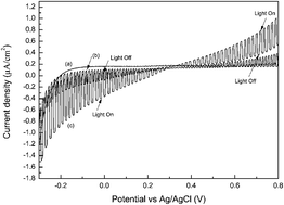
Melem and its derivatives were synthesized from melamine by a two-step heat treatment method between 400 and 650 °C in air. It was demonstrated that such polymeric C–N semiconductors possess a photoelectrochemical (PEC) conversion effect with both photocathodic and photoanodic characteristics, which was proposed to be caused by the formation of tri-s-triazine ring. The dimelem synthesized at 450 °C exhibited the highest PEC conversion activity. The possible reasons were discussed. The unique bidirectional photocurrent generation makes melem and its derivatives attractive photoelectrochemical materials.


1. Introduction

An energy shortage is one of the most serious challenges faced by human beings, which has a direct bearing on the sustainable development of our society.1 Among the multitudinous technologies to deal with this challenge, photoelectrochemical (PEC) cells are a good choice to convert clean solar energy into electrical energy or storable, transportable chemical fuels.1,2 During the past 40 years, a variety of n-type metal oxide semiconductors have been widely researched as photoanodic materials for PEC water oxidation, such as TiO2, ZnO, Fe2O3, BiVO4, Zn2SnO4, etc.3–7 However, the p-type semiconductors that could be used as photocathodic materials for PEC water reduction are seldom reported.8 Recently, it has been reported that graphitic carbon nitride (g-C3N4), a metal-free polymeric semiconductor, can be used as a photocathodic material for chemical fuels.9 In fact, compared with other polymeric semiconductors, g-C3N4 possesses a series of properties, such as a low price, a high thermal and chemical stability in air, a suitable band edge position, which make it a very promising material for solar energy systems.10 Many researchers have focused on the preparation and characterization of g-C3N4. Considering the semiconductor property of g-C3N4 is originated from the tri-s-triazine rings in the polymer structure, we expect the intermediates towards g-C3N4, also containing the tri-s-triazine rings, may possess similar PEC activity. Up to now, the investigations of PEC activities of intermediates during condensation of melamine to g-C3N4 have not been reported to our knowledge.

In this paper, we prepared melem and its derivatives by treating melamine in air between 400 and 650 °C by a two-step heat treatment method. Photoelectrochemical activities of the as-prepared products were investigated in a conventional three-electrode cell. As a result, all of the products showed both cathodic and anodic photocurrents, indicating that they could be used as either photocathodic or photoanodic materials.

2. Experimental

2.1. Synthesis process

All chemicals used in this research were analytical grade and used as received without further treatment. Melamine was purchased from Sinopharm Chemical Reagent Co., Ltd. In a typical synthetic procedure of melem and its derivatives, melamine (3 g) was put into a crucible with cover. The crucible was placed in a muffle furnace, which was heated to the pre-established temperature ranging from 400 to 650 °C at a rate of 10 °C min−1, and then kept at this temperature for 2 hours. After that, the products were cooled to room temperature with furnace naturally. In order to get pure products, the obtained products were ground and treated for another 2 hours at the same temperature. Finally, the white or yellow products were again ground into powder in agate mortar and stored in different sample bottles. The as-prepared samples were named as M-x, where x was referred to the treating temperature.

2.2. Characterization

The crystalline phase and structure of the products were analyzed with X-ray diffraction (XRD, Bruker D8) using Cu Kα irradiation source. The bonding structures were analyzed with a Fourier transform infrared spectrometer (FTIR, PerkinElmer Frontier). The optical properties were measured with a UV/VIS/NIR spectrometer (PerkinElmer, Lamda 950). For this measurement, the product powders were fixed by two quartz plates, one of which contained a rectangular groove. The diffuse reflection spectra were recorded with a calibrated total-reflection white plate at the rear, while the transmission spectrum was neglected. The absorption spectrum could be calculated by A = 1 − R, where R was the diffuse reflectance. The Kubelka–Munk function F(R) was calculated by F(R) = (1 − R)2/2R. The band gap of the products were deduced by [F(R)]n = Eg, where n was 1/2 for indirect band gap and 2 for direct band gap semiconductor.10 The BET surface areas of the products were measured by N2 absorption at 77 K on an ASAP 2010 instrument. The microstructures of the products were observed with scanning electron microscope (SEM, Hitachi, S-4700).

The photoelectrochemical activities were investigated using an electrochemical analyzer (CHI-660D Shanghai Chenhua, China) with a conventional three-electrode cell, where a platinum wire was used as the counter electrode and an Ag/AgCl (saturated KCl) electrode as the reference electrode. The incident light was taken from a solar simulator (AM 1.5, 100 mW cm−2, CEL-S500, Ceaulight, China). The working electrode (photoelectrode) was prepared on Sn-doped In2O3 (ITO) glass substrates. At first, 10 mg of powder was ground for 5 min in agate mortar and then mixed with 100 μL of H2O. 20 μL of PEDOT:PSS (Sigama-Aldrich, 2.8 wt%) was added or not for different photoelectrodes. The mixture was pestled for another 5 min to get homogeneous slurry. The slurry was then spread onto 1 cm2 of ITO glass substrate (length 2.5 cm and width 1 cm) with a glass rod, using adhesive tapes as spaces. After air-drying, the film was annealed at 150 °C for 12 min in air to improve the adhesion. The film thickness measured by optical microscopy was about 10 μm. The working electrode was immersed in a 0.1 M KCl aqueous solution, and the glass side was faced to the incident light.

3. Result and discussion

The structures of the M-x samples condensed at different temperatures are first evaluated by XRD. From Fig. 1, it can be seen that the material obtained at 400 °C, namely M-400 can be attributed to melem.11,12 When the polymerization temperature reaches 500 °C, two typical peaks for graphitic-like layered structures are observed, which are located around 13.0° and 27.4°, respectively. It has been reported that the peak around 27.4° is a characteristic interplanar stacking peak of aromatic systems,13 which is indexed as the (002) peak, with the corresponding d-spacing to be 0.326 nm. The peak around 13.0° is related to an in-plane structural packing motif,13 corresponding to a distance d = 0.678 nm. M-500 can be assigned to be melon, which is also in agreement with the following FTIR analysis.12,13 With the further increase of polymerization temperature, the FWHM of (002) peaks becomes narrower and the corresponding diffraction angle shifts towards high-angle direction, implying the interplanar spacing becomes smaller, slightly. It can be inferred that upon 550 °C condensation, the obtained products, carbon nitrides, contain graphitic-like layered structure, just like melon.
image file: c5ra02816g-f1.tif
Fig. 1 XRD patterns of the M-x samples.

The structural information of melamine and the prepared samples are provided by FTIR spectra. In Fig. 2, the spectrum of melamine observed in our experiment is in agreement with data reported by related literature.14 The absorption bands at 3470, 3418, 3328, 3125 cm−1 are attributed to NH2 stretch vibration, while the band located at 1649 is assigned to NH2 bend vibration. The bands at 1540, 1469, 1431 cm−1 are assigned to side-chain asymmetric C–N stretch vibration, side-chain C–N breath vibration and ring stretch, respectively. The strong band at 811 cm−1 is assigned to the ring-sextant out-of-plane bend vibration. As for M-400, three major absorption bands are observed at 1602, 1460 and 802 cm−1, which are the characteristic of the tri-s-triazine ring.15 This means the formation of melem when the condensation temperature reaches 400 °C, which is in accordance with our XRD result. At about 450 °C, the three main absorption bands located at 1602, 1460 and 802 cm−1 remain, while a few new peaks at 1403, 1327, 1252 cm−1 (ν(C–N) of aromatic secondary and tertiary amines16) occur. This means that the structure of melem is changed and a new kind of material forms by the connection of two adjacent melem molecules, which can be assigned to dimelem, an intermediate from melem to melon as shown in Fig. 3.13 As for M-500, melon, the observed spectrum in Fig. 2 is in accordance with the spectrum reported in the literature.15 In the case of M-550, no obvious differences can be observed, compared with melon. Further increasing the temperature, the intensities of bands at 1318, 1232, 1209 cm−1 corresponding to trigonal C–N(–C)–C are enhanced, which indicates the formation of a more condensed carbon nitride polymer.17 It should not be ignored that the weak absorption band around 3167 cm−1 duo to ν(N–H) suggests the residual of little hydrogen in the products.


image file: c5ra02816g-f2.tif
Fig. 2 FTIR spectra of melamine and the M-x samples.

image file: c5ra02816g-f3.tif
Fig. 3 Possible reaction pathway for the formation of melem and its derivatives by thermal condensation of melamine.

The optical properties of the synthesized samples are investigated by the UV-vis DRS. A typical absorption pattern of a semiconductor is observed for all M-x samples in Fig. 4a. Obviously, the absorption edges of the samples exhibit the red shift with the increase of condensation temperature, which is in accordance with the gradual change in colour from white to dark yellow. It has been reported that the optical properties of the products are dominated by the tri-s-triazine nucleus, from melem to carbon nitride polymers.12,15 The optical band gap of the samples are calculated according to literatures as indirect band gap materials.13,15,18 The results are shown in Fig. 4b. Eg decreases with the increase of temperature, due to the increase of polymerization degree. An approximate linear equation may be concluded as Eg(t) = 3.4228–0.0014t, where t is in degrees Celsius. “Tail-up” phenomenon between 450 and 600 nm in the absorption spectra occurs perhaps due to the defects formed during the heating processes, especially at T ≥ 600 °C.13,19


image file: c5ra02816g-f4.tif
Fig. 4 (a) UV-vis spectra and (b) optical band gap of the M-x samples.

IV curves of photocurrent response at different electrodes are presented in Fig. 5. The dimelem photoelectrode shows either cathodic or anodic photocurrents at different range of electrode potential, and the onset potential is about 0.3 V. This phenomenon is quite different from that of typical bulk semiconductors, where either anodic or cathodic photocurrent is observed at n-type and p-type semiconductors, respectively. Generally, the conduction type of semiconductors can be identified by this method.6,7 To clarify the generation mechanism of photocurrent at dimelem photoelectrode, the IV curve of ITO is also measured and shown in Fig. 5. It can be seen that the only anodic photocurrent formed at ITO electrode is quite small, which results from the photocatalyzed oxidation of Cl by holes accumulated at the surface of ITO.20 Therefore, the formation of both cathodic and anodic photocurrents at dimelem electrode is mainly due to the existence of the organic semiconductor, dimelem. It is also observed that the cathodic and anodic photocurrents both increase dramatically when PEDOT:PSS, a hole-transport material, is added during the process of preparing electrode. It is considered that PEDOT:PSS not only enhances the adhesion between ITO glass and dimelem film, but also increases the separation efficiency of photogenerated excitons by the formation of donor–acceptor construction.10


image file: c5ra02816g-f5.tif
Fig. 5 Current–potential curves of (a) ITO, (b) ITO/M-450 (dimelem), (c) ITO/PEDOT:PSS/M-450 in 0.1 M KCl.

In order to compare the PEC activities of the as-synthesized samples, M-x, the current–potential curves of corresponding electrodes are measured and shown in Fig. S1. Interestingly, all the samples show cathodic and anodic photocurrents, especially for melem and dimelem. On the other hand, M-450, namely dimelem, produces the highest photocurrent. Then with the further increase of temperature, the photocurrent produced by corresponding sample decreases gradually as we can see from Fig. S2. It should be pointed out that the BET surface area increases from 3.9 m2 g−1 to 9.8 m2 g−1 with the increase of temperature as shown in Table S1.

It has been reported that the wavefunction of the valence band for polymeric melon is a combination of the HOMO levels of the melem monomer and the conduction band may be assigned to the LUMO of the melem monomer. The HOMO of melem is derived from heterocyclic nitrogen pz orbitals, and LUMO mainly consists of carbon pz orbitals.19 The redox potentials of H+/H2 and Cl2/Cl couples lie between the band-edge positions of melem and its derivatives.19,21 Besides, it has been proven that the difference between the Fermi level and the valence band of g-C3N4 is (1.5 ± 0.3) eV, which is a proof for an intrinsic g-C3N4 semiconductor.22 On the basis, a preliminary generation mechanism of photocurrent is proposed, as shown in Fig. 6.


image file: c5ra02816g-f6.tif
Fig. 6 Generation mechanism of photocurrent (a) anodic photocurrent; (b) cathodic photocurrent.

The bidirectional photocurrents start to appear after the melem structure is formed at 400 °C. As for melem and its derivatives, this PEC activity may be originated from the tri-s-triazine rings due to its band structure. The photocurrent reaches the maximum for dimelem, which probably relates to the unique nanowire shape of dimelem as shown in Fig. S3. The nanowire morphology promotes the transport and separation of photogenerated carriers by shortening the transport distance, resulting in a higher PEC activity, as shown in Fig. S4.23 Besides, the photocurrents are prompt, steady and reproducible during light on/off for cycles, as shown in Fig. S5. The BET surface area is not the major factor according to our results. Secondly, dimelem is the intermediate product between single tri-s-triazine rings and conjugated tri-s-triazine rings. In fact at this intermediate condensation temperature, a mixture of single and conjugated tri-s-triazine rings can be formed, which may form heterojunctions in situ due to the Fermi level difference, thus improve the charge separation. Such heterojunctions might exist for all the intermediate phases during the transition of melamine to the ideal graphitic carbon nitride using the current method. When the heating temperature is too low or too high, one component will dominate, and therefore, the number of heterojunctions decreases, resulting in the decreasing photocurrents.

4. Conclusions

In this study, melem and its derivatives with different photo response were synthesized by treating melamine between 400 and 650 °C by a two-step heating method. They all show cathodic and anodic photocurrents, indicating the potential as photocathodic or photoanodic materials. The PEC activities of melem and its derivatives may be originated from tri-s-triazine rings. The bidirectional photocurrents generation of melem and its derivatives are considered to be different from that of typical n-type or p-type bulk semiconductors. In particular, dimelem obtained at 450 °C contains the highest PEC activity due to promoted transport and separation efficiency of photogenerated carriers.

Acknowledgements

The authors thank Dr Junlin Du for assistance in the photoelectrochemistry experiments. We also thank Dr Jiantao Bian and Jian Yu for the helpful discussions. This work was supported by the Main Direction Program of Knowledge Innovation of Chinese Academy of Sciences (no. KGCX2-YW-399+11).

Notes and references

  1. M. Grätzel, Nature, 2001, 414, 338 CrossRef PubMed.
  2. A. Fujishima and K. Honda, Nature, 1972, 238, 37 CrossRef CAS.
  3. M. Xu, P. M. Da, H. Y. Wu, D. Y. Zhao and G. F. Zheng, Nano Lett., 2012, 3, 1503 CrossRef PubMed.
  4. A. Wolcott, W. A. Smith, T. R. Kuykendall, Y. P. Zhao and J. Z. Zhang, Adv. Funct. Mater., 2009, 19, 1849 CrossRef CAS.
  5. D. K. Zhong, J. W. Sun, H. Inumaru and D. R. Gamelin, J. Am. Chem. Soc., 2009, 131, 6086 CrossRef CAS PubMed.
  6. M. C. Long, W. M. Cai and H. Kisch, J. Phys. Chem. C, 2008, 112, 548 CAS.
  7. M. A. Alpuche-Aviles and Y. Y. Wu, J. Am. Chem. Soc., 2009, 131, 3216 CrossRef CAS PubMed.
  8. F. Odobel, L. L. Pleux, Y. Pellegrin and E. Blart, Acc. Chem. Res., 2010, 43, 1063 CrossRef CAS PubMed.
  9. Y. J. Zhang, Z. Schnepp, J. Y. Cao and S. Q. Liu, Sci. Rep., 2013, 3, 2163 Search PubMed.
  10. Y. J. Zhang and M. Antonietti, Chem.–Asian J., 2010, 5, 1307 CAS.
  11. B. Jürgens, E. Irran, J. Senker and P. Kroll, J. Am. Chem. Soc., 2003, 125, 10288 CrossRef PubMed.
  12. T. Tyborski, C. Merschjann, S. Orthmann and F. Yang, J. Phys.: Condens. Matter, 2012, 24, 162201 CrossRef CAS PubMed.
  13. A. Thomas, A. Fischer, F. Goettmann and M. Antonietti, J. Mater. Chem., 2008, 18, 4893 RSC.
  14. M. K. Marchewka, Mater. Sci. Eng., B, 2002, 95, 214 CrossRef.
  15. A. I. Finkel'shtein and N. V. Spiridonova, Russ. Chem. Rev., 1964, 33, 400 CrossRef PubMed.
  16. T. Komatsu, J. Mater. Chem., 2001, 11, 802 RSC.
  17. B. V. Lotsch, M. Döblinger, J. Sehnert and W. Schnick, Chem.–Eur. J., 2007, 13, 4969 CrossRef CAS PubMed.
  18. Y. Wang, Y. Di, M. Antonietti, H. R. Li, X. F. Chen and X. C. Wang, Chem. Mater., 2010, 22, 5119 CrossRef CAS.
  19. X. C. Wang, K. Maeda, A. Thomas and K. Takanabe, Nat. Mater., 2009, 8, 76 CrossRef CAS PubMed.
  20. L. I. Halaoui, J. Electrochem. Soc., 2003, 150, E455 CrossRef CAS PubMed.
  21. Y. J. Cui, Z. X. Ding, P. Liu, M. Antonietti, X. Z. Fu and X. C. Wang, Phys. Chem. Chem. Phys., 2012, 14, 1455 RSC.
  22. F. Yang, M. Lublow, S. Orthmann, C. Merschjann, T. Tyborski, M. Rusu, M. Kanis, A. Thomas, R. Arrigo, M. Hävecker and T. Schedel-Niedrig, ChemSusChem, 2012, 5, 1227 CrossRef CAS PubMed.
  23. X. H. Li, J. S. Zhang, X. F. Chen, A. Fischer, A. Thomas, M. Antonietti and X. C. Wang, Chem. Mater., 2011, 23, 4344 CrossRef CAS.

Footnotes

Electronic supplementary information (ESI) available: See DOI: 10.1039/c5ra02816g
Current affiliation: Institute of Advanced Photovoltaics, Fujian Jiangxia University, Fuzhou 350108, China. E-mail: E-mail: yqiu78@hotmail.com.

This journal is © The Royal Society of Chemistry 2015
Click here to see how this site uses Cookies. View our privacy policy here.