Electrically controllable microstructures and dynamic light scattering properties of liquid crystals with negative dielectric anisotropy
Huihui Wang†
a,
Ling Wang†a,
Hui Xiead,
Chenyue Lia,
Shumeng Guoa,
Meng Wangb,
Cheng Zoub,
Dengke Yang*c and
Huai Yang*ab
aDepartment of Materials Physics and Chemistry, School of Materials Science and Engineering, University of Science and Technology Beijing, Beijing 100083, People's Republic of China
bDepartment of Materials Science and Engineering, College of Engineering, Peking University, Beijing 100871, People's Republic of China. E-mail: yanghuai@pku.edu.cn
cChemical Physics Program and Liquid Crystal Institute, Kent State University, Kent, Ohio 44242, USA. E-mail: Dyang@kentvm.kent.edu
dSchool of Chemistry and Materials Science, Gui Zhou Normal University, Guiyang, Guizhou, P. R. China
First published on 31st March 2015
Abstract
In this paper thin films which can potentially function as novel electrically switchable shutters were fabricated based on a commercially available liquid crystal media with negative dielectric anisotropy, and their microstructures and dynamic light scattering properties were investigated in detail by the in situ formation of polymer networks. It was found that the light transmittance of the prepared films in the wavelength range from 400 nm to 3000 nm can be expediently controlled on demand by felicitously applying an electric field with an appropriate strength. Compared to the ultraviolet (UV) and visible (Vis) regions, the light transmittance in the near infrared (NIR) region was much higher when a voltage over 30 V was applied. Continually raising the applied voltage would, however, increase the NIR transmittance without noticeable changes in the UV and Vis regions. Furthermore, we have also explored the relationship between the dynamic light scattering properties and the corresponding microstructures of the polymer network. The velocity of the flow of dynamic scattering increased with the increase of the applied voltage, which led to the gradual appearance of large sized pores followed by oversized connected pores with many tiny holes in the boundary. Accordingly, the dynamic light scattering of the samples increased with the increasing microstructures of the polymer network.
1. Introduction
Liquid crystals (LCs) are self-organized dynamic functional soft materials which possess both order and mobility at molecular, supramolecular and macroscopic levels.1 With LCs displays ubiquitous in our daily life, the research and development of LCs are moving rapidly into beyond-display applications, such as optical communication, optical data storage, beam steering, etc.2 Compared to the conventional mechanical photonic devices, LCs-based ones offer an enormous number of blueprints for device designs, fabrications and applications due to their fast response, small size, reduced weight, low power consumption and so forth.3–6 Reversible switching between the light-scattering and the light-transmittance mode of LCs with negative dielectric anisotropy undoubtedly represents such an elegant system. When an appropriate direct current (DC) or low-frequency alternating current (AC) filed is applied to a nematic LCs (NLCs) thin-film possessing negative dielectric anisotropy, the William's domains are supposed to form at the low voltage state, and then the microdomains would break up into swarms if exceeding the threshold value. These turbulent swarms are able to scatter the light, so-called dynamic scattering.7–10A variant of the NLCs is the cholesteric LCs (CLCs), which spontaneously forms a macroscopic helical structure either when the LC molecules are inherently chiral or when chirality is externally introduced. Due to their unique photonic nanostructures, CLCs have been widely used for fabrication of stable random lasers.11–13 One key benefit of using CLCs in the development of random lasers is their response to electric fields. At low frequencies, flow of ions results in the breaking up of the layers to form a scattering texture which remains stable after the removal of the electric field. Upon application of a high-frequency electric field, clear homeotropic orientation of the molecules is obtained.
As a result, achieving great potential for applications will require controlling directly different scattering states by alteration of the applied electric field. This, in turn, will require a fundamental understanding of the LCs molecular movement during dynamic scattering and the factors which determine the microstructure and light scattering properties. LCs/polymer composites have attracted increasing interest over the last years, not only due to their promising properties for reflective display applications based on polymer-stabilized cholesteric textures, but also with respect to fundamental insights concerning pre-transitional phenomena and elastically induced properties.14 The composites are obtained by dissolving a relatively small amount of a bifunctional photo-reactive (mesogenic) monomer, generally between 1–10 wt%, in a low-molar-mass LCs host material, together with a photo-initiator. The monomer molecules align along the LCs director field and are subsequently polymerized by UV irradiation of the sample. The polymer network prepared in this in situ polymerization method can potentially act as the template for the self-organized LCs order and director configuration for various systems, including nematic, cholesteric, smectic, even 3D blue phases.15–20
Herein, we reported the electrically controllable microstructures and dynamic light scattering in LCs with negative dielectric anisotropy loaded with salt-type dopant. To explore the relationship between the LCs microstructures and the dynamic light scattering properties under different electric fields, the in situ polymer networks of the LCs director configuration were successfully achieved. Firstly, the change in the alignment of NLCs system for different applied voltage at fixed frequency was studied. Then, the microstructure of the polymer network was investigated by electrically control, which effected on the tendency of the light scattering intensity. Although, CLCs system exhibits a similar light scattering behavior to NLCs system, they can selective reflect circularly polarized incident light with the same handedness as its helical axis on account of the unique helical supramolecular structure for some applications. The microstructure with different pitches of the CLCs was investigated in order to understand the relationship between the microstructure and the light scattering properties. Importantly, electrically controllable dynamic light scattering across the wavelength region from 400 nm to 3000 nm was fully investigated based on the combination of three kinds of classical light scattering theories: the Rayleigh–Gans (RG) approach, the anomalous diffraction (AD) approach, and the geometrical optics (GO) approach.21–23
2. Experimental
2.1 Materials
The LCs used in the study were SLC10V513-200 (TNI = 365.2 K, Δε = −11.2, Shijiazhuang Chengzhi Yonghua Display Materials Co. Ltd.), the chiral dopant R811 (Merck Co., Ltd) were used. The monomer was a di-functional monomer C6M (Merck). Hexadecyl trimethyl ammonium bromide (Sinopharm Chemical Reagent Co. Ltd.) salt was employed. The photoinitiator was Irgacure 651 (Ciba-Geigy). All of the above materials were used as received without further purification.2.2 Sample preparation
The compositions of the samples were prepared and vigorously stirred until a homogeneous mixture formed. Then, the mixture was sandwiched between two pieces of indium–tin-oxide coated glass substrates by capillary filling into LC cell. The film thickness was controlled by 30.0 ± 1.0 μm thick polyester spacers. In order to observe the microscopic structure of the samples, they were irradiated for polymerisation by a UV lamp (365 nm 35 W Hg lamp, PS135, UV Flood, Stockholm, Sweden) for 10.0 min at 318.2 K. The compositions of samples in the study are listed in Table 1.| Sample | NLCs (wt%) | R811 (wt%) | Monomers (wt%) | Photoinitiator (wt%) | Salt (wt%) |
|---|---|---|---|---|---|
| 1 | 94.6 | 0.0 | 7.0 | 0.3 | 0.1 |
| 2 | 74.3 | 20.3 | 7.0 | 0.3 | 0.1 |
| 3 | 84.5 | 10.1 | 7.0 | 0.3 | 0.1 |
| 4 | 87.8 | 6.8 | 7.0 | 0.3 | 0.1 |
| 5 | 88.6 | 6.0 | 7.0 | 0.3 | 0.1 |
2.3 Measurements
The morphology of the samples was observed by scanning electron microscopy (SEM) (ZEISS, EVO18, Germany). The samples were first separated and dipped into cyclohexane for four days at room temperature to extract the LCs molecules, followed by drying for 12 hours under vacuum. After the samples were sputtered with carbon, the microstructure of the polymer network was observed under SEM. The optical textures of the samples used were studied by polarizing optical microscopic (POM) (Olympus BX-51) equipped with function generator (Tektronix AFG3102) and RF Power Amplifier (NF HSA4051). The spectra of selective transmission were obtained by UV/VIS/NIR spectrophotometer (JASCO V-590), while the transmittance of the blank cell was normalized as 100%.3. Results and discussion
3.1 Effect of the electric field changes on the microstructure of NLCs with negative dielectric anisotropy on dynamic scattering
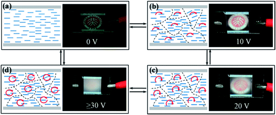
As described by the Carr–Helfrich mechanism, the formation of anomalous alignment and convective flow cells is the responses of the NLCs to external fields. In this paper, the behaviour of the LCs in a low frequency (Hz) electric field was studied. The subsequent behaviour is then described in terms of voltages. As the voltage is increased, at some fixed frequency below the cut-off frequency, the system undergoes various transitions from straight or oblique convective rolls to less symmetrical patterns.24,25 Hence, the change in the alignment of the NLCs (sample 1) for different applied voltage at fixed frequency of 100 Hz was illustrated schematically in Fig. 1. Assuming that the sample 1 was initially in the parallel state appearing transparent in Fig. 1(a), when a low voltage (E = 10 V) was applied, a scattering texture formed and evolved microdomains as a result of the turbulent motion of the ionic species, due to the competition of the conductivity and dielectric torques. It was noted that the scattering texture appeared to be less opaque in the case than that observed when the sample was without applying electric in Fig. 1(b). With a subsequent increase of the applied voltage, the microdomains began to form roll-like pattern, along with transmittance of the samples decreasing in Fig. 1(c). When the applied voltage was increased to 30 V, the roll-like domains began to appear everywhere. The sample appeared white in Fig. 1(d). It should be also noted that the transformation between any states was reversible and repeatedly driven many times without noticeable fatigue.The results of observations with POM were shown in Fig. 2. Fig. 2(a) shows the appearance of domains at the applied an ac field of the order of 10 V. The domain structure in space was clear and found an isogyre in the each cellular domain. These domains resembled of the circular domains. As shown in Fig. 2(b), increasing the applied voltage at 20 V, two neighbouring domains were fused into an elongated one as roll-like. The organization process of a new dissipative structure was activated by increasing the applied electric field. Thus the roll-like domains began to appear everywhere, when we increased further the applied voltage from 30 V to 60 V in Fig. 2(c–f). We also found that a dust particle flows periodically between a domain centre and a domain boundary in a cellular domain. The velocity of the flow of it increased with the increasing of the applied voltage.
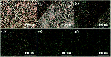 | ||
| Fig. 2 Optical polarizing microscopy textures of sample 1 under different operating voltage environments: (a) 10 V, (b) 20 V, (c) 30 V, (d) 40 V, (e) 50 V, and (f) 60 V. | ||
The sample 1 was sealed and irradiated with an UV source (2.0 mW cm−2) for 10.0 min to induce the in situ polymerization with applied voltage at 10 V, 20 V, 30 V, 40 V, 50 V, and 60 V, respectively. Fig. 3 shows the microstructure of the polymer network of sample 1 with different applied voltage. It can be clearly seen that the changes of the applied voltage dramatically alter the network structure. At voltage of E = 10 V, it appeared to be upward or downward in similar to wave. With increasing the applied voltage, polymer networks containing round bore with dimensions approximately 3 to 10 μm were observed in Fig. 3(b). When the applied voltage increased to 30 V, a series of oversize connected pores occurring could be funded which dimensions reach up to 30 μm. At the same time, many tiny holes were founded in boundary. With the further increase of the applied voltage, the oversize connected pores occurred were not vertically stacks but had tilted a certain angle between upper substrate. Moreover, the quantity of oversize connected pores decreased with increasing the number of tiny holes. The probability of molecular collision increased forming more tiny holes, because the velocity of the flow of the films increased with the increasing of the applied voltage. The above confirmed that the LCs microdomains where the turbulent motion of the ionic species occurred could be easily controlled by just applying different voltage.
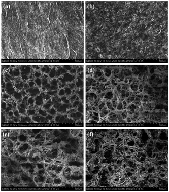 | ||
| Fig. 3 Scanning electron microscopy images of sample 1 under different operating voltage environments: (a) 10 V, (b) 20 V, (c) 30 V, (d) 40 V, (e) 50 V, and (f) 60 V. | ||
3.2 Effect of the electric field changes on the microstructure of CLCs with negative dielectric anisotropy on dynamic scattering
CLCs also exhibit light scattering states; however, unlike with NLCs, it is possible for the strong multiple scattering states to remain once the applied electric field is removed. CLCs have been shown to be particularly effective materials in which scattering can be readily induced by electrical means at low voltages for fabrication of stable random lasers.In order to achieve great potential for applications, we pay attention on studying effect of the electric field changes on the microstructure of CLCs with negative dielectric anisotropy. Additional POM of the sample 3 texture with different applied electric field are shown in Fig. 4 to highlight the different textures that were formed. These images represent the states of the sample applied electric field at 0 V, 10 V, 30 V, and 50 V, respectively. The sample was initially in the parallel state in Fig. 4(a), if a low voltage (E = 10 V) is applied, the swarm formation was almost instantaneous in Fig. 4(b). Fig. 4(c and d) show the optical texture for voltages of E = 30 V and E = 50 V respectively. The dynamic scattering state was observed with the field applied which was found to increase in velocity of the flow as the voltage was increasing.
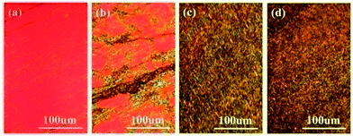 | ||
| Fig. 4 Optical polarizing microscopy textures of sample 3 under different operating voltage environments: (a) 0 V, (b) 10 V, (c) 30 V and (d) 50 V. | ||
Fig. 5 shows the microstructure of the polymer network of sample 3 by UV initiation polymerization with applied voltage at 30 V, 50 V, 70 V, and 90 V, respectively. As shown in Fig. 5(a), polymer networks containing round bore with dimensions approximately 10 μm were observed. With increasing applied voltage, polymer networks appear regions of “bulklike” were founded in Fig. 5(b). At 70 V applied voltage, open network composed of discrete, rice-grain-like particles were observed in Fig. 5(c). With the further increasing of the applied voltage, polymer networks were loose network by contrast in Fig. 5(d).
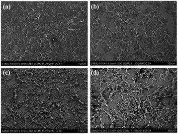 | ||
| Fig. 5 Scanning electron microscopy images of sample 3 under different operating voltage environments: (a) 30 V, (b) 50 V, (c) 70 V and (d) 90 V. | ||
As is well-known, the molecules of CLCs assembled layered in spiral with a torsion angle between layer and layer. Assuming that the sample was initially in the parallel state, if a low voltage (E < 30 V) was applied, electrohydrodynamic instability accompanied with the flows just occur in the single molecular layer. If, instead, a voltage above E = 30 V was applied, the molecules responded dielectrically to act synergistically in microdomains between layer and layer with the direction of the applied electric field.
3.3 Effect of the variations pitch on the microstructure of CLCs with negative dielectric anisotropy on dynamic scattering
The CLCs contains helical domains in which the orientation vector successively turns a small torsion angle from one layer to the next one along the helical axis. These helical domains can selectively reflect some wavelength light (λ). The relationship between wavelength and pitch (P) of domains can be described by the following equation:λmax = nP![[thin space (1/6-em)]](https://www.rsc.org/images/entities/char_2009.gif) sin sin![[thin space (1/6-em)]](https://www.rsc.org/images/entities/char_2009.gif) θ θ |
Pitch plays an important role in dynamic scattering and further optimization of the light scattering intensity is a prerequisite for satisfactory electro-optical characteristics. Fig. 6 shows the microstructure of the polymer network of samples 2–5 by UV initiation polymerization with applied voltage at 70 V, respectively. Here, the chiral monomer was right-handed helix. The samples contained chiral dopant R811, thus, the position of the reflection band can be adjusted by choosing an appropriate concentration of R811. The network voids became smaller with the decrease of the pitch as shown in Fig. 6. It's possible that because molecules respond dielectrically to act synergistically in microdomains were not individual molecules but molecular group matching one cholesteric pitch to happen electrohydrodynamic instability accompanied with the flows. Here, the cholesteric pitch corresponds to length over which the director rotates 360°. There may be evidence that the polymer morphology ensures memory effects of the orientational order present when its formation occurs.
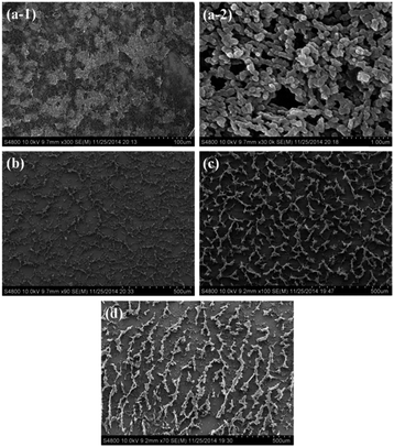 | ||
| Fig. 6 Scanning electron microscopy photographs of samples at 70 V: (a) sample 2, (b) sample 3, (c) sample 4 and (d) sample 5. | ||
3.4 Light scattering properties of the LCs with negative dielectric anisotropy on dynamic scattering
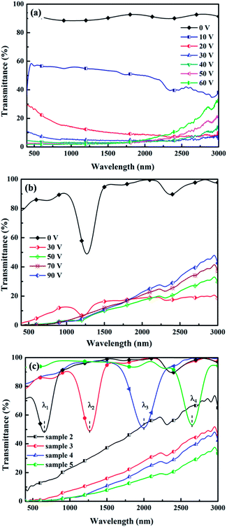
Fig. 7(a and b) show the wavelength (λ) dependence of the off-state transmittance for samples 1 and 2 with different applied voltage, respectively. As shown in Fig. 7(a), if a low voltage (E < 30 V) was applied, the transmittance of the samples decreased with the increasing applied voltage in the wavelength range of 400 nm to 3000 nm. For comparison, the transmittance of the sample only about 8% wavelength range of 400 nm to 3000 nm can be transmitted at the voltage of E = 30 V. If, instead, a voltage E > 30 V was applied, the transmittance of the samples in NIR region was higher than that of the samples in UV and VIS regions, increasing with the increasing applied voltage in the wavelength range of 1300 nm to 3000 nm. The similar to the tendency of transmittance for CLCs with increasing applied voltage in Fig. 7(b). Fig. 7(c) shows the wavelength (λ) dependence of the off-state transmittance for samples 2–5. λ1, λ2, λ3 and λ4 respectively correspond to P1, P2, P3 and P4 that gradually increased in pitch. It can be obviously seen that the transmittance of the samples decreased with the increasing length of CLCs pitch in the wavelength range of 400 nm to 3000 nm.Above-mentioned phenomenas can be explained by three approximate approaches concerning the light scattering properties of dynamic scattering: the RG approach, the AD approach, and the GO approach.26–29 The RG approximation for light scattering is appropriate for submicron-sized scattering particles, and is shown to describe accurately the scattering properties of very small LCs droplets, as well as that of small polymer crystallites. The scattering intensity τ is defined by
| τ ∝ D3/λ4 | (1) |
For large weakly scattering center particles, the light scattering property can be studied by AD theory, τ is defined by
| τ ∝ D/λ2 | (2) |
When the scattering center particle size is larger than the scale of the wavelength of light, the light scattering property can be studied by GO theory, τ is defined by
| τ ∝ 1/(Dλn)(0 ≤ n ≤ 4) | (3) |
According to the eqn (1), it can be explained that the τ of sample 1 with applied voltage at 10 V is very low, due to the polymer network containing submicron-sized pores result in an insufficient number of scattering centers, which is in good agreement with our experimental result in Fig. 3(a). According to the eqn (1)–(3), we can speculate large bore appeared and then the quantity of that gradually increased. Finally, oversize pores formed with many tiny holes. Various sizes of pores were nonlinear distribution in polymer network of sample 1 with the increasing applied voltage. These results are in good agreement with our experimental result in Fig. 3(b–f). In the same way, we can speculate what the distributions of pores were in polymer network of sample 3 with different applied voltage based on the equations. Moreover, the variation tendency of the light scattering intensity for samples 2–5 at the applied voltage of 70 V with the equations enable to infer their microstructures, as shown in Fig. 7(c). Consequently, the scattering intensity in the wavelength range of 400–3000 nm could be controlled with different scattering states by alteration of the applied electric field. The theoretical approaches have directive significance to our experiment.
4. Conclusions
In conclusion, the electrically controllable microdomains and dynamic light scattering in negative liquid crystals loaded with salt-type dopant were investigated. The films were clear and did not give rise to scattering of light. When an electric field was applied across the films, scattering of the light could be induced. The intensity of the transmitted light decreased with increasing voltage. The microstructure of the samples was found that have a pronounced effect on the light scattering properties from the films. Films formed by NLCs showed the transmittance decreased with the increasing applied voltage, while the transmittance in NIR region was higher than that of the films in UV and VIS regions at E > 30 V. The similar to the tendency of transmittance for films formed by CLCs with increasing applied voltage, but it also decreased with the increasing length of the CLCs pitch. Additionally, the relationship between microdomains of the LCs and the light scattering properties was discussed based on RG approach, the AD approach, and the GO approach. The research disclosed herein is expected to provide a unique prospect for precisely regulating the microstructures of thin films according to the desired functional properties, paving way for the widespread applications in areas of military or civil safety as well as opto-electronic devices.Acknowledgements
This work was supported by the Sino-American Cooperative Project of Chinese Ministry of Science and Technology under Grant (2013DFB50340), the National Natural Science Foundation of China (NSFC) (Grant no. 51173003, Grant no. 51333001), the Major Program of Chinese Ministry of Education under Grant (313002), the Doctoral Fund of Chinese Ministry of Education under Grant (20120001130005).Notes and references
- H. K. Bisoyia and S. Kumar, Chem. Soc. Rev., 2011, 40, 306 RSC.
- Q. Li, Liquid Crystals Beyond Displays: Chemistry, Physics, and Applications, John Wiley & Sons, Hoboken, New Jersey, 2012 Search PubMed.
- M. Peccianti, C. Conti, G. Assanto, A. D. Luca and C. Umeton, Appl. Phys. Lett., 2002, 81, 3335 CrossRef CAS PubMed.
- M. W. P. L. Baars, M. C. W. Boxtel, C. W. M. Bastiaansen, D. J. Broer, S. H. M. Söntjens and E. W. Meijer, Adv. Mater., 2000, 12, 715 CrossRef CAS.
- M. Ohe and K. Kondo, Appl. Phys. Lett., 1995, 67, 3895 CrossRef CAS PubMed.
- S. H. Lee, S. L. Lee and H. Y. Kim, Appl. Phys. Lett., 1998, 73, 2881 CrossRef CAS PubMed.
- R. Chang, J. Appl. Phys., 1973, 44, 1885 CrossRef CAS PubMed.
- W. Helfrich, J. Chem. Phys., 1969, 51, 4092 CrossRef CAS PubMed.
- A. Sussman, Appl. Phys. Lett., 1972, 21, 126 CrossRef CAS PubMed.
- G. H. Heilmeier, L. A. Zanoni and L. A. Barton, IEEE Trans. Electron Devices, 1970, ED-17, 22 CrossRef PubMed.
- S. M. Morris, A. D. Ford, M. N. Pivnenko and H. J. Coles, J. Appl. Phys., 2005, 97, 0h23103 CrossRef PubMed.
- B. He, Q. Liao and Y. Huang, Opt. Mater., 2008, 31, 375 CrossRef CAS PubMed.
- S. M. Morris, D. J. Gardiner, M. M. Qasim, P. J. W. Hands, T. D. Wilkinson and H. J. Coles, J. Appl. Phys., 2012, 111, 033106 CrossRef PubMed.
- I. Dierking, Adv. Mater., 2003, 15, 152 CrossRef CAS.
- R. W. Guo, K. X. Li, H. Cao, X. J. Wu, G. J. Wang, Z. H. Cheng, F. F. Wang, H. Q. Zhang and H. Yang, Polymer, 2010, 51, 5990 CrossRef CAS PubMed.
- J. B. Guo, H. Cao, J. Wei, D. W. Zhang, F. Liu, G. H. Pan, D. Y. Zhao, W. L. He and H. Yang, Appl. Phys. Lett., 2008, 93, 201901 CrossRef PubMed.
- W. Hu, H. Y. Zhao, L. Song, Z. Yang, H. Cao, Z. H. Cheng, Q. Liu and H. Yang, Adv. Mater., 2010, 22, 468 CrossRef CAS PubMed.
- X. W. Chen, L. Wang, Y. Y. Chen, C. Y. Li, G. Y. Hou, X. Liu, X. G. Zhang, W. L. He and H. Yang, Chem. Commun., 2014, 50, 691 RSC.
- L. Wang, W. L. He, X. Xiao, F. G. Men, Y. Zhang, P. Y. Yang, L. P. Wang, J. M. Xiao, H. Yang and Y. F. Lu, Small, 2012, 8, 2189 CrossRef CAS PubMed.
- L. Wang, W. L. He, Q. Wang, M. N. Yu, X. Xiao, Y. Zhang, M. Ellahi, D. Y. Zhao, H. Yang and L. Guo, J. Mater. Chem. C, 2013, 1, 6526 RSC.
- G. P. Montgomery, J. L. West and T. L. Winifred, J. Appl. Phys., 1991, 69, 1605 CrossRef PubMed.
- V. A. Loiko and A. V. Konkolovich, J. Exp. Theor. Phys., 2003, 96, 489 CrossRef CAS.
- G. P. Crawford, D. W. Allender and J. W. Doane, Phys. Rev. A, 1992, 45, 8693 CrossRef CAS.
- D. K. Rout and R. N. P. Choudhary, J. Phys. D: Appl. Phys., 1989, 22, 289 CrossRef CAS.
- G. H. Heilmeier, L. A. Zanoni and L. A. Barton, Proc. IEEE, 1968, 56, 1162 CrossRef.
- S. J. Cox, V. Y. Reshetnyak and T. J. Sluckin, J. Phys. D: Appl. Phys., 1998, 31, 1611 CrossRef CAS.
- J. B. Whitehead, S. Zumer and J. W. Doane, J. Appl. Phys., 1993, 73, 1057 CrossRef CAS PubMed.
- W. B. Li, H. Cao, M. K. Kashima, F. Liu, Z. H. Cheng, Z. Yang, S. Q. Zhu and H. Yang, J. Polym. Sci., Part B: Polym. Phys., 2008, 46, 2090 CrossRef CAS.
- W. B. Li, Z. H. Cheng, G. H. Pan, H. J. Liu, H. Cao, Z. Yang and H. Yang, Opt. Mater., 2008, 31, 434 CrossRef CAS PubMed.
Footnote |
| † Huihui wang and Ling wang contributed equally to this work. |
| This journal is © The Royal Society of Chemistry 2015 |

