DOI:
10.1039/C5RA01787D
(Paper)
RSC Adv., 2015,
5, 35506-35512
Enhancing photoelectrochemical activity of CdS quantum dots sensitized WO3 photoelectrodes by Mn doping†
Received
2nd February 2015
, Accepted 18th March 2015
First published on 18th March 2015
Abstract
Mn-doped CdS quantum dots sensitized WO3 photoelectrodes were successfully synthesized by a combination of hydrothermal and chemical bath deposition (CBD) methods. To improve the stability of the photoelectrodes in an alkaline environment, the electrodes were treated with TiCl4 to form a nano-TiO2 buffer layer on the WO3 plate surface before depositing CdS quantum dots (QDs). The resulting electrodes were applied as photoanodes in the photoelectrochemical cell for water splitting. The photoelectrochemical (PEC) properties were investigated by the photocurrent density curves and incident photon-to-current conversion efficiency (IPCE). The as-prepared Mn-CdS QDs sensitized WO3 plate-like photoelectrodes exhibit a significant improvement in their photoelectrochemical performance compared with undoped photoelectrodes. To better understand the enhanced PEC properties, the electron transport properties and efficient electron lifetime were studied in detail using electrochemical impedance spectroscopy (EIS), transient photocurrent spectroscopy and intensity modulated photocurrent spectroscopy (IMPS). The results show that the Mn-CdS QDs/TiO2/WO3 photoelectrodes exhibit a higher electron transit rate and a longer electron lifetime. This is most likely due to the existence of electronic states in the mid-gap region of the Mn-CdS QD.
1. Introduction
Hydrogen gas is considered to be a potential candidate for one of the most clean energy sources due to its renewable and environmental friendly characteristics.1 Since the first report on the photoelectrochemical water splitting for hydrogen production using a titanium dioxide (TiO2) photoelectrode in 1971,2 many studies have been dedicated to develop suitable photoelectrode materials, such as ZnO,3,4 Fe2O3,5,6 Cu2O7,8 and WO3, for converting solar energy into hydrogen.9,10 Among these materials, tungsten trioxide (WO3), which exhibits high photo-catalytic activity, chemical stability in acidic solutions and a nontoxic nature, is known as a promising material.10,11 Unfortunately, its large band gap (Eg ≥ 2.6 eV) limits the energy absorption in the near UV region.12 A large number of approaches have been taken to improve the activity of WO3 in the visible light region.13–15 A good solution could be the construction of a heterostructure junction between the narrow bandgap semiconductor and the wide bandgap semiconductor, which provides significant advantages for light absorption.16–19 Therefore, several types of heterostructures, such as BiVO4/WO3,20 Fe2O3/WO3,21 NiWO3/WO3,22 InVO4/WO3 (ref. 23) and CdS/WO3,24,25 have been demonstrated to be potential candidates to improve the photocatalytic activity of WO3.
Among the various narrow bandgap semiconductor materials, CdS quantum dots (QDs) are a well-known semiconductor material that have been widely used as photosensitizers for various wide bandgap semiconductor photoanodes.26–28 CdS QDs have been paid much attention due to their specific advantages, including the appropriate band gap (Eg ≈ 2.4 eV) and suitable valence band position.29,30 CdS QDs sensitized wide bandgap semiconductor electrodes, such as CdS QDs/TiO2,31,32 CdS QDs/ZnO,33,34 CdS QDs/BiVO4 (ref. 35) and CdS QDs/WO3,36 showed enhanced visible light absorption and improved water splitting performance. Many efforts, including the use of bilayer electrodes37–39 and co-sensitization together with infrared QDs (PbS,40 CdSe27 and Ag2S41), have been devoted to further improve the performance of CdS QDs-based photoelectrodes. Recently, the synthesis of Mn doped CdS (Mn-CdS) has been proven to be a powerful strategy to extend the lifetime of charge carriers to boost the efficiency of QDs-sensitized solar cells.42
In this study, we first report an investigation on the Mn-CdS QDs sensitized WO3 plate-like photoelectrodes and their performance for PEC hydrogen generation. The high-density arrays of monoclinic single crystalline WO3 plates were grown directly on FTO by a hydrothermal method. The conformal coating of a nano-TiO2 buffer layer on WO3 plates was carried out by the thermal hydrolysis of TiCl4. The Mn-CdS QDs were deposited on the plate-like film by the CBD technique. The structural, morphological and photoelectrochemical properties of the photoelectrodes were evaluated.
2. Experimental section
2.1 Synthesis and characterization
The WO3 plate-like films were synthesized by a hydrothermal method according to our previous study.43 0.231 g of Na2WO4·2H2O was dissolved in 30 mL of ultrapure water under constant stirring at room temperature. Then, 10 mL of 3 M HCl was added to the solution, followed by the addition of 0.2 g of (NH4)2C2O4. After five minutes of stirring, 30 mL of ultrapure water was added into the solution with continual stirring for 30 min. The as-prepared precursor was transferred into a 100 mL of Teflon-lined autoclave. The FTO substrates with the conducting side facing down were immersed and leaned against the wall of the Teflon vessel. The hydrothermal synthesis was conducted at 140 °C for 3 h. The as-prepared films were annealed at 450 °C for 2 h. The conformal coating of the nano-TiO2 buffer layer on WO3 plates was carried out by the thermal hydrolysis of TiCl4, which was described in the reported literature.44 Mn-CdS QDs were deposited on the plate-like film by the CBD technique. Firstly, the substrates with WO3 plate-like films were immersed in an ethanol solution containing 5 mM Cd(NO3)2 and 3.75 mM manganese acetate for 5 min for the adsorption of Cd2+ and Mn2+ on the WO3 plates surface and then thoroughly washed with anhydrous ethanol. Then, they were dipped in a 5 mM methanol solution of Na2S for 5 min and washed with methanol at least three times. This two-step dipping procedure was repeated ten times. The as-prepared films were calcined at 200 °C for 1 h.
Scanning electron microscopy (SEM, Nova NanoSEM 230) was utilized to observe the morphology and size of the products. High-resolution transmission electron microscopy (HR-TEM, TECNAI G2 F20, FEI) was operated at 200 kV to observe the crystallinity and distribution of WO3, TiO2 and Mn-CdS. The crystalline phases of the synthesized products were characterized by an X-ray diffractometer (XRD, D/Max2250, Rigaku Corporation, Japan). The surface electronic states of the films were analyzed using X-ray photoelectron spectroscopy (XPS, K-Alpha 1063, Thermo Fisher scientific). A spectrophotometer (DR-UVS, Shimadzu 2450 spectrophotometer) was used to obtain the UV-vis spectra in the 300–800 nm range.
2.2 Electrical and photoelectrochemical measurements
The photoelectrochemical response of the samples was recorded with an electrochemical analyzer (Zennium, Zahner, Germany) using a typical three-electrode electrochemical cell. An Ag/AgCl/satd. KCl electrode and a platinum foil were employed as the reference electrode and the counter electrode, respectively. An aqueous solution containing 0.35 M Na2SO3 and 0.25 M Na2S (pH ≈ 11.5) was used as electrolyte and sacrificial reagent to maintain the stability of CdS QDs, respectively. A 150 W Xe lamp (CHF-XM35, Beijing Trusttech Co. Ltd) with an ultraviolet filter (λ > 400 nm) to remove UV irradiation was used as the visible light source and positioned 10 cm away from the photoelectrochemical cell. The light intensity was adjusted to 100 mW cm−2. Intensity modulated photocurrent spectroscopy (IMPS) measurements were obtained using a Zahner CIMPS-2 system. A white light lamp emitting diode (λ = 520 nm) driven by a PP210 was used as a lamp.
3. Results and discussion
3.1 XRD, SEM, EDS, HR-TEM and XPS analysis
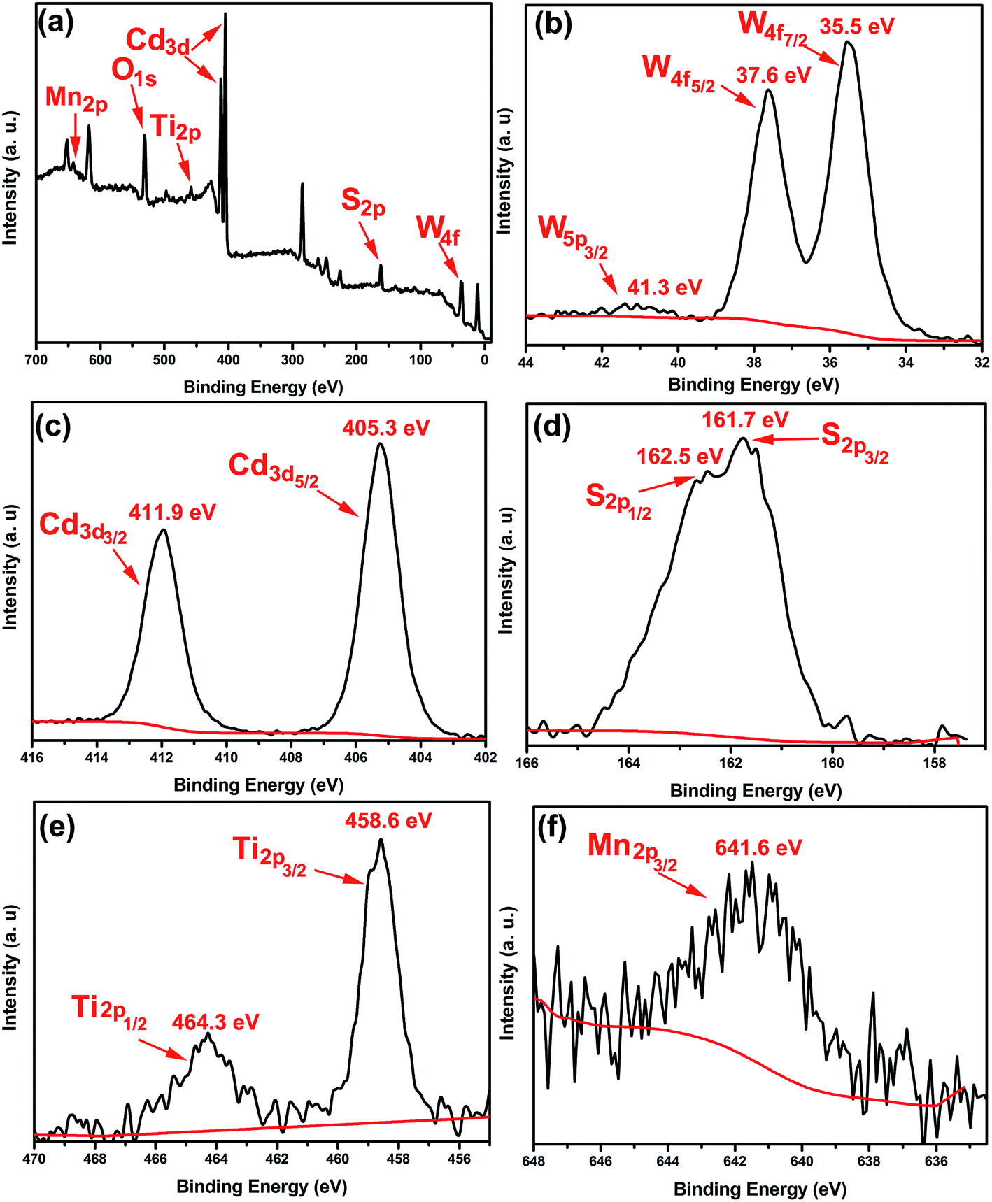
The crystal structures of the sample electrodes were examined by XRD analysis. Fig. 1 shows the XRD patterns of WO3 film, TiO2/WO3 film, CdS QDs/TiO2/WO3 film and Mn-CdS QDs/TiO2/WO3 film. The patterns of all the films present the same peaks, corresponding to monoclinic WO3 (JCPDS no. 83-0950). Unfortunately, there are no other obvious peaks in the patterns, which is likely due to the low TiO2, CdS and Mn-CdS content. The morphologies of the sample films were examined by field emission scanning electron microscopy (FESEM). Fig. 2 displays the typical top-view FESEM images of the WO3 plate-like film at low and high magnification. It can be seen that the high density and uniform vertical alignment of WO3 plates are grown on a FTO substrate. All the WO3 plates exhibit an edge length in the range of 0.5–1.5 μm and a thickness of 50–200 nm. As compared to pristine WO3 plates with a smooth surface, the TiO2/WO3 plates exhibit a rough surface (Fig. 2a and b). This is because a number of nano-TiO2 flakes and dots were aggregated to form a thin film on the surface of the plates after TiCl4 treatment. After loading CdS QDs and Mn-CdS QDs, the number of dots obviously increased, which can be observed in Fig. 2c and d. The TEM image of a Mn-CdS QDs/TiO2/WO3 plate in Fig. 3a shows that the Mn-CdS QDs are uniformly distributed on the entire TiO2/WO3 plate surface to form a high-quality WO3/Mn-CdS core–shell nanoplate. The spatial chemical compositions of Mn-CdS QDs/TiO2/WO3 plate were identified by the EDS spectrum, which shows the existence of Mn, Cd, S, and Ti elements on the WO3 plates, as shown in Fig. 3b. The composition of the Mn-CdS QDs/TiO2/WO3 film was further detected by XPS, as shown in Fig. 4. The survey XPS spectrum is shown in Fig. 4a, which contains the peaks of W4f, S2p, Cd3d, Ti2p and O1s. The peaks centered at 41.3 eV, 37.6 eV and 35.5 eV are attributed to W6+ (Fig. 4b), and the peaks at 464.3 eV and 458.6 eV are attributed to Ti2p (Fig. 4e). In addition, the peaks at 405.3 eV and 411.9 eV correspond to Cd3d and at 161.7 eV and 162.5 eV correspond to S2p (Fig. 4c and d). Importantly, the Mn2p peak can be observed at 641.5 eV (Fig. 4f), which is in good agreement with the reported study.45 On the basis of the abovementioned results, it can be confirmed that Mn has been successfully doped into the CdS QDs.
 |
| | Fig. 1 XRD patterns of the film samples. | |
 |
| | Fig. 2 SEM images of (a) WO3 film, (b) TiO2/WO3 film, (c) CdS QDs/TiO2/WO3 film and (d) Mn-CdS QDs/TiO2/WO3 film. | |
 |
| | Fig. 3 (a) TEM images and (b) EDS spectra of Mn-CdS QDs/TiO2/WO3 film. | |
 |
| | Fig. 4 XPS spectra analysis of Mn-CdS QDs/TiO2/WO3 film, (a) wide scan for Mn-CdS QDs/TiO2/WO3 film, narrow scan for (b) W element, (c) Cd element, (d) S element, (e) Ti element (f) Mn element. | |
3.2 UV-visible optical absorption
Fig. 5 illustrates the UV-visible optical absorption spectra of the TiO2/WO3, QDs CdS/TiO2/WO3 and Mn-QDs CdS/TiO2/WO3 film. The spectrum obtained from the TiO2/WO3 film shows that the adsorption edge of the TiO2/WO3 film is located at ∼455 nm. By the in situ growth of CdS QDs in the WO3 plate-like film, the absorption spectrum was extended into the visible light region with a band edge of more than 530 nm due to the CdS QDs absorption. Relative to the absorption edge of the QDs CdS/TiO2/WO3 film, the absorption edge of Mn-QDs CdS/TiO2/WO3 film shows a slight red-shift and a little enhancement in the visible light region, which is consistent with what is reported in previous study.46 The images of the sample films shown in Fig. S1† also support the abovementioned result. There is no obvious difference in color between the pristine WO3 film and the TiO2/WO3 film. Compared with the former two samples, the color of the WO3 films sensitized by QDs evidently changed to orange. The Mn-QDs CdS/TiO2/WO3 film is slightly darker than the QDs CdS/TiO2/WO3 film.
 |
| | Fig. 5 UV-visible optical absorption spectral of the film samples. | |
3.3 Photoelectrochemical study
To confirm the potential advantages of the Mn-CdS QDs/TiO2/WO3 film as a photoanode, four types of photoanodes with Mn-CdS QDs/TiO2/WO3, CdS QDs/TiO2/WO3, TiO2/WO3 and WO3 were fabricated on FTO glass for comparison. The linear sweep voltammograms of the four photoanodes are compared in Fig. 6a. These measurements were carried out in dark and under illumination of AM 1.5 (with UV cutoff) at 100 mW cm−2. Under light illumination, the TiO2/WO3 and WO3 photoanodes show negligible photocurrent generation, while Mn-CdS QDs/TiO2/WO3 and CdS QDs/TiO2/WO3 photoanodes exhibit significant photocurrent generation. This indicates that the large photocurrents can be attributed to electrons generated from CdS QDs. Among them, the maximum photocurrent density of 2.51 mA cm−2 was obtained with Mn-CdS QDs/TiO2/WO3 photoanodes at 0 V vs. Ag/AgCl, which is about 10 times larger than that of the bare WO3 photoanodes (0.24 mA cm−2) and about 7 times larger than that of the TiO2/WO3 photoanodes (0.34 mA cm−2). Furthermore, the Mn-CdS QDs/TiO2/WO3 photoanodes present better photoelectrochemical properties than those of CdS QDs/TiO2/WO3 photoanodes (1.40 mA cm−2).
 |
| | Fig. 6 (a) The photocurrent density and (b) IPCE of the photoelectrodes. | |
The incident photon-to-current conversion efficiencies (IPCE) of the photoelectrodes were measured at an applied voltage of −0.4 V vs. Ag/AgCl, and the results are shown in Fig. 6b. As expected from the absorption edge of TiO2/WO3 films, the TiO2/WO3 electrodes show the photoresponse only at the wavelength of ∼452 nm with a lower IPCE value of ∼15%. Compared to TiO2/WO3 electrodes, the electrodes sensitized by QDs show substantially enhanced IPCE in a wide range (from 350 to 550 nm) due to the increased light absorption by the QDs. More importantly, the IPCE value of the Mn-CdS QDs/TiO2/WO3 electrodes is the highest, which is in accordance with the photocurrent results.
To better understand the enhanced PEC properties in the Mn-CdS QDs/TiO2/WO3 photoelectrodes, the electron transport properties and the efficient electron lifetime were assessed using electrochemical impedance spectroscopy (EIS). EIS is an effective method to investigate electrochemical behavior, especially for charge transfer processes. The EIS Nyquist plots are related to the charge transfer resistance and the separation efficiency of the photoelectron–hole pairs.47 Fig. 7 shows the EIS Nyquist plots of CdS QDs/TiO2/WO3 and Mn-CdS QDs/TiO2/WO3 photoelectrodes at the applied potential of −0.2 V vs. Ag/AgCl under visible light illumination. The EIS Nyquist plots is fitted by the equivalent circuit (the inset in Fig. 7) composed of a charge transfer resistance (R1), a chemical capacitance (CPE1) and a series resistance (RS). R1 corresponds to the complex charge transfer resistance in the photoelectrode, and RS represents the sheet resistance of the FTO glass, contact resistance, and wire resistance.48 The electron lifetimes (τe) could be estimated using the following formula: τe = R1CPE1.28 A larger τe means that the electrons have a longer lifetime and a faster diffusion rate in the electrode.49 As listed in Table 1, the RS values of the two samples are similar, while the R1 values are very different. The R1 value of the Mn-CdS QDs/TiO2/WO3 photoelectrode is only 1/2 of that of the CdS QDs/TiO2/WO3 photoelectrodes, implying that Mn-doped-CdS greatly promotes the charge transport and suppresses the electron–hole recombination, which is consistent with the improved PEC property. Moreover, the Mn-CdS QDs/TiO2/WO3 photoelectrodes (497.3 ms) have a 2-fold longer τe compared with CdS QDs/TiO2/WO3 (1101 ms). This is due to the existence of electronic states in the midgap region of the Mn-CdS QD, resulting in the long-lived charge carriers and the retarded charge pair recombination.42 It was also supported by the transient photocurrent plots (Fig. S2†), which indicates that the addition of Mn2+ into a crystal lattice of CdS QDs prolongs the lifetime of the photogenerated electron–hole pairs.
 |
| | Fig. 7 Electrochemical impedance spectra of the photoelectrodes. | |
Table 1 Equivalent circuit parameters of EIS for CdS QDs/TiO2/WO3 and Mn-CdS QDs/TiO2/WO3 photoelectrodes
| Samples |
Rs (Ω cm2) |
R1 (Ω cm2) |
CPE1 (μF) |
τe (ms) |
| CdS QDs/TiO2/WO3 |
34.45 |
1318 |
377.3 |
497.3 |
| Mn-CdS QDs/TiO2/WO3 |
27.30 |
617.1 |
1784 |
1101 |
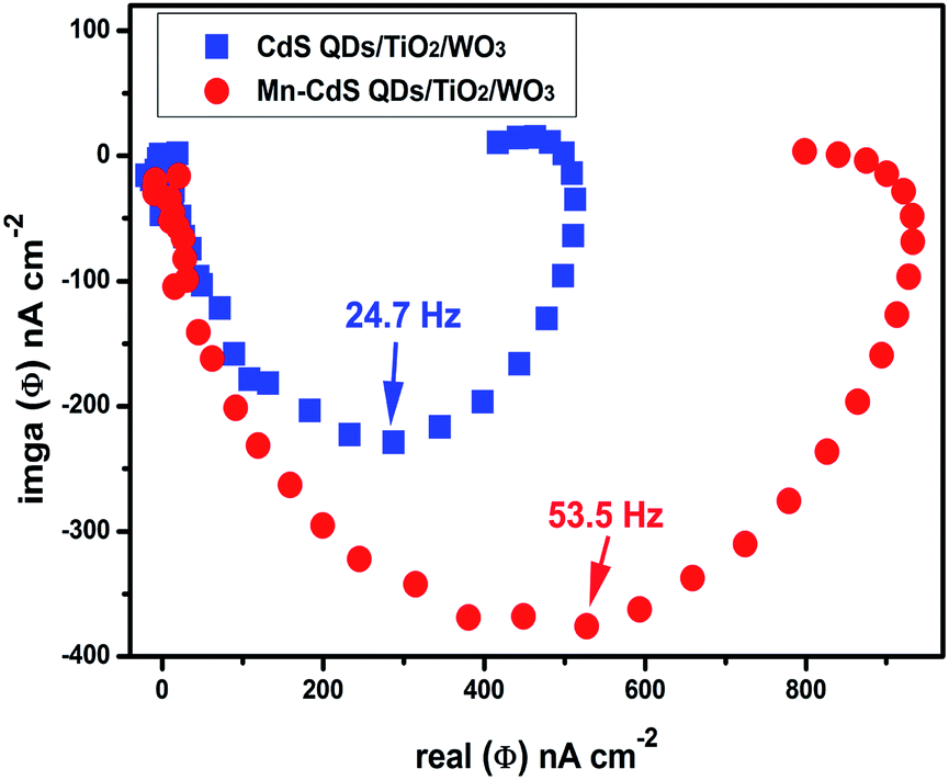
In order to further characterize the electron transport properties and support the abovementioned ideas, intensity-modulated photocurrent spectroscopy (IMPS) measurements were employed. During the IMPS measurements, the photoelectrodes were biased at −0.2 V (vs. Ag/AgCl) and illuminated with a white light emitting diode (λ = 520 nm) at 2.19 mW cm−2. The IMPS plots of the sample photoelectrodes are shown in Fig. 8. The electron transport time (τd) can be estimated from the IMPS plots, according to the following formula: τd = (2πfmin)−1, where fmin is the characteristic minimum frequency of the imaginary component of IMPS.50,51 The electron transport times calculated for Mn-CdS QDs/TiO2/WO3 and CdS QDs/TiO2/WO3 electrodes are 2.98 ms and 6.45 ms, respectively. This result suggests that the Mn-CdS QDs/TiO2/WO3 photoelectrodes exhibit a higher electron transit rate than CdS QDs/TiO2/WO3 photoelectrodes, which supports the EIS results very well.
 |
| | Fig. 8 Complex plane plot of the IMPS response of the photoelectrodes. | |
The schematic for the Mn-CdS QDs/TiO2/WO3 electrode illustrates the electron transfer process, which can explain the possible mechanism for the enhanced photoelectrochemical properties under visible light irradiation (Fig. 9). The conduction band value of the CdS QDs is −0.4 eV, which is above that of TiO2 (−0.1 eV) and WO3 (+0.4 eV), according to previous works.52 In the CdS QDs/TiO2/WO3 system, when the electron–hole pairs are generated in CdS QDs under visible light illumination, the photoexcited electrons can be separated from the holes by transfer to TiO2 and then to WO3 along the potential gradient. In the Mn-CdS QDs/TiO2/WO3 system, the electronic states in the midgap region of the CdS QD can be created by Mn doping. The photoexcited electrons can easily migrate to the electronic states in the midgap region of the Mn-CdS QD, and then to TiO2 and WO3 (as shown in the schematic in Fig. 9).42 The electronic states in the midgap region of the Mn-CdS QD can be used as the buffer level state. This induces long-lived charge carriers and retards the recombination of charge pairs, thereby resulting in enhancing PEC performance.
 |
| | Fig. 9 Sketch showing the architecture of the Mn-CdS QDs/TiO2/WO3 photoelectrodes and electron-transfer processes. | |
4. Conclusion
In summary, we have synthesized Mn-doped CdS quantum dots sensitized WO3 photoelectrodes by a combination of hydrothermal and CBD methods. The results of EDS and XPS demonstrated that Mn was indeed incorporated into the crystal lattice of CdS. The SEM and TEM images showed that the Mn-CdS QDs were uniformly deposited on the surface of the TiO2/WO3 plates. The results show that the Mn-CdS QDs/TiO2/WO3 electrodes exhibit excellent PEC activities, which is attributed to the existence of electronic states in the midgap region of the Mn-CdS QD, resulting in the long-lived charge carriers and the retarded charge pair recombination.
Acknowledgements
This study was supported by the National Nature Science Foundation of China (no. 21171175), China Scholarship Council (CSC File no. 201406370157) and the Fundamental Research Funds for the Central Universities of Central South University (2014zzts015).
References
- J. A. Turner, Science, 2004, 305, 972–974 CrossRef CAS PubMed.
- A. Fujishima and K. Honda, Nature, 1972, 238, 37–38 CrossRef CAS.
- A. Wolcott, W. A. Smith, T. R. Kuykendall, Y. Zhao and J. Z. Zhang, Adv. Funct. Mater., 2009, 19, 1849–1856 CrossRef CAS PubMed.
- H. Chen, Z. Wei, K. Yan, Y. Bai, Z. Zhu, T. Zhang and S. Yang, Small, 2014, 10, 4760–4769 CrossRef CAS PubMed.
- A. A. Tahir, K. G. U. Wijayantha, S. Saremi-Yarahmadi, M. Mazhar and V. McKee, Chem. Mater., 2009, 21, 3763–3772 CrossRef CAS.
- H. Dotan, K. Sivula, M. Grätzel, A. Rothschild and S. C. Warren, Energy Environ. Sci., 2011, 4, 958 CAS.
- Y.-K. Hsu, C.-H. Yu, Y.-C. Chen and Y.-G. Lin, Electrochim. Acta, 2013, 105, 62–68 CrossRef CAS PubMed.
- Y.-K. Hsu, C.-H. Yu, Y.-C. Chen and Y.-G. Lin, J. Power Sources, 2013, 242, 541–547 CrossRef CAS PubMed.
- G. Hodes, D. Cahen and J. Manassen, Nature, 1976, 260, 312–313 CrossRef CAS.
- X. Liu, F. Wang and Q. Wang, Phys. Chem. Chem. Phys., 2012, 14, 7894–7911 RSC.
- D. V. Esposito, J. G. Chen, R. W. Birkmire, Y. Chang and N. Gaillard, Int. J. Hydrogen Energy, 2011, 36, 9632–9644 CrossRef CAS PubMed.
- B. Cole, B. Marsen, E. Miller, Y. Yan, B. To, K. Jones and M. Al-Jassim, J. Phys. Chem. C, 2008, 112, 5213–5220 CAS.
- Y. Sun, C. J. Murphy, K. R. Reyes-Gil, E. A. Reyes-Garcia, J. M. Thornton, N. A. Morris and D. Raftery, Int. J. Hydrogen Energy, 2009, 34, 8476–8484 CrossRef CAS PubMed.
- W. Li, J. Li, X. Wang and Q. Chen, Appl. Surf. Sci., 2012, 263, 157–162 CrossRef CAS PubMed.
- Y. C. Nah, I. Paramasivam, R. Hahn, N. K. Shrestha and P. Schmuki, Nanotechnology, 2010, 21, 105704 CrossRef PubMed.
- B. Wang, J. Zhang, Y. Hu, S. Wang, R. Liu, C. He, X. Wang and H. Wang, Int. J. Electrochem. Sci., 2013, 8, 7175–7186 CAS.
- Y. J. Hwang, A. Boukai and P. Yang, Nano Lett., 2008, 9, 410–415 CrossRef PubMed.
- J. Schrier, D. O. Demchenko, L. W. Wang and A. P. Alivisatos, Nano Lett., 2007, 7, 2377–2382 CrossRef CAS PubMed.
- N. S. Lewis, Science, 2007, 315, 798–801 CrossRef CAS PubMed.
- J. Su, L. Guo, N. Bao and C. A. Grimes, Nano Lett., 2011, 11, 1928–1933 CrossRef CAS PubMed.
- K. Sivula, F. L. Formal and M. Grätzel, Chem. Mater., 2009, 21, 2862–2867 CrossRef CAS.
- J. Zhu, W. Li, J. Li, Y. Li, H. Hu and Y. Yang, Electrochim. Acta, 2013, 112, 191–198 CrossRef CAS PubMed.
- F. Zhang, W. Zhao and K. Zhang, React. Kinet., Mech. Catal., 2013, 108, 253–261 CrossRef CAS PubMed.
- H.-i. Kim, J. Kim, W. Kim and W. Choi, J. Phys. Chem. C, 2011, 115, 9797–9805 CAS.
- Z.-G. Zhao, Z.-F. Liu and M. Miyauchi, Adv. Funct. Mater., 2010, 20, 4162–4167 CrossRef CAS PubMed.
- L. M. Peter, D. J. Riley, E. J. Tull and K. G. U. Wijayantha, Chem. Commun., 2002, 1030–1031 RSC.
- G. Wang, X. Yang, F. Qian, J. Z. Zhang and Y. Li, Nano Lett., 2010, 10, 1088–1092 CrossRef CAS PubMed.
- H. Chen, L. Zhu, H. Liu and W. Li, Electrochim. Acta, 2013, 105, 289–298 CrossRef CAS PubMed.
- H. Chen, L. Zhu, Q. Hou, W. Liang, H. Liu and W. Li, J. Mater. Chem., 2012, 22, 23344–23347 RSC.
- J. Deng, M. Wang, X. Song, Y. Shi and X. Zhang, J. Colloid Interface Sci., 2012, 388, 118–122 CrossRef CAS PubMed.
- Y. Hu, B. Wang, J. Zhang, T. Wang, R. Liu, J. Zhang, X. Wang and H. Wang, Nanoscale Res. Lett., 2013, 8, 1–5 CrossRef PubMed.
- F. Su, J. Lu, Y. Tian, X. Ma and J. Gong, Phys. Chem. Chem. Phys., 2013, 15, 12026–12032 RSC.
- H. Chen, W. Li, H. Liu and L. Zhu, Sol. Energy, 2010, 84, 1201–1207 CrossRef CAS PubMed.
- M. Thambidurai, N. Muthukumarasamy, N. Sabari Arul, S. Agilan and R. Balasundaraprabhu, J. Nanopart. Res., 2011, 13, 3267–3273 CrossRef CAS.
- J. Jiang, M. Wang, R. Li, L. Ma and L. Guo, Int. J. Hydrogen Energy, 2013, 38, 13069–13076 CrossRef CAS PubMed.
- C. Liu, Y. Li, W. Li, J. Zhu, J. Li, Q. Chen and Y. Yang, Mater. Lett., 2014, 120, 170–173 CrossRef CAS PubMed.
- S. Buhbut, S. Itzhakov, E. Tauber, M. Shalom, I. Hod, T. Geiger, Y. Garini, D. Oron and A. Zaban, ACS Nano, 2010, 4, 1293–1298 CrossRef CAS PubMed.
- S. Buhbut, S. Itzhakov, D. Oron and A. Zaban, J. Phys. Chem. Lett., 2011, 2, 1917–1924 CrossRef CAS.
- B. Wang, H. Ding, Y. Hu, H. Zhou, S. Wang, T. Wang, R. Liu, J. Zhang, X. Wang and H. Wang, Int. J. Hydrogen Energy, 2013, 38, 16733–16739 CrossRef CAS PubMed.
- H. J. Lee, P. Chen, S. J. Moon, F. Sauvage, K. Sivula, T. Bessho, D. R. Gamelin, P. Comte, S. M. Zakeeruddin, S. I. Seok, M. Gratzel and M. K. Nazeeruddin, Langmuir, 2009, 25, 7602–7608 CrossRef CAS PubMed.
- I. Hwang, M. Seol, H. Kim and K. Yong, Appl. Phys. Lett., 2013, 103, 023902 CrossRef PubMed.
- P. K. Santra and P. V. Kamat, J. Am. Chem. Soc., 2012, 134, 2508–2511 CrossRef CAS PubMed.
- J. Yang, W. Li, J. Li, D. Sun and Q. Chen, J. Mater. Chem., 2012, 22, 17744 RSC.
- H. Zheng, Y. Tachibana and K. Kalantar-zadeh, Langmuir, 2010, 26, 19148–19152 CrossRef CAS PubMed.
- D. S. Kim, Y. J. Cho, J. Park, J. Yoon, Y. Jo and M.-H. Jung, J. Phys. Chem. C, 2007, 111, 10861–10868 CAS.
- J. Luo, H. Wei, Q. Huang, X. Hu, H. Zhao, R. Yu, D. Li, Y. Luo and Q. Meng, Chem. Commun., 2013, 49, 3881–3883 RSC.
- L. Wu, J. Li, S. Zhang, L. Long, X. Li and C. Cen, J. Phys. Chem. C, 2013, 117, 22591–22597 CAS.
- X. Miao, K. Pan, Y. Liao, W. Zhou, Q. Pan, G. Tian and G. Wang, J. Mater. Chem. A, 2013, 1, 9853–9861 CAS.
- C. Zha, L. Shen, X. Zhang, Y. Wang, B. A. Korgel, A. Gupta and N. Bao, ACS Appl. Mater. Interfaces, 2013, 6, 122–129 Search PubMed.
- H. Chen, Z. Wei, K. Yan, Y. Bai and S. Yang, J. Phys. Chem. Lett., 2014, 5, 2890–2896 CrossRef CAS.
- J. Su, L. Guo, N. Bao and C. A. Grimes, Nano Lett., 2011, 11, 1928–1933 CrossRef CAS PubMed.
- D. Robert, Catal. Today, 2007, 122, 20–26 CrossRef CAS PubMed.
Footnotes |
| † Electronic supplementary information (ESI) available. See DOI: 10.1039/c5ra01787d |
| ‡ Contributed equally to this work. |
|
| This journal is © The Royal Society of Chemistry 2015 |
Click here to see how this site uses Cookies. View our privacy policy here.