Band engineering and charge separation in the Mo1−xWxS2/TiO2 heterostructure by alloying: first principle prediction

M. Farajia, M. Sabzalia, S. Yousefzadeha, N. Sarikhanib, A. Ziashahabia, M. Ziraka and A. Z. Moshfegh*ac
aDepartment of Physics, Sharif University of Technology, Tehran, 11155-9161, Iran. E-mail: moshfegh@sharif.edu; Tel: +98-21-66164516
bSchool of Mechanical Engineering, Sharif University of Technology, Tehran, 11155-9567, Iran
cInstitute for Nanoscience and Nanotechnology, Sharif University of Technology, Tehran, 14588-89694, Iran

Received 7th January 2015 , Accepted 12th March 2015

First published on 16th March 2015


Abstract

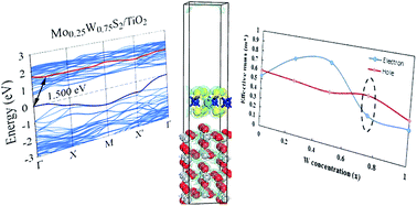
The composition dependent electronic properties of the Mo1−xWxS2 monolayer deposited over a TiO2 (110) substrate were investigated based on ab initio density functional calculations by applying periodic boundary conditions. Adsorption of the Mo1−xWxS2 monolayer on the TiO2 is physical in nature based on calculated binding energy values. It was found that the mechanical strain generated by the presence of TiO2 beneath the Mo1−xWxS2 layer resulted in a shift in band position of the Mo1−xWxS2 in favor of photoelectrochemical water splitting. Moreover, variation of W concentration in Mo1−xWxS2 could improve the charge separation and increase the effective mass ratio leading to an extension of the electron–hole pair lifetime which is useful for photocatalytic and photoelectrochemical applications.


1. Introduction

Several years after the pioneering work of Fujishima and Honda1 on the water splitting reaction at photoinduced titanium dioxide crystals, efforts to improve the properties of TiO2 and other photocatalysts have remained an important issue. TiO2, as a wide band gap semiconductor, is one of the most attractive photocatalysis and photovoltaic materials that has been investigated for solar energy conversion, as well as water and air purification, extensively.2 Under ultraviolet irradiation (<387 nm), whose energy exceeds the band gap of 3.3 eV in the anatase crystalline phase, TiO2 is highly active and chemically stable. Efforts to reduce the band gap energy of TiO2 have been carried out by many researchers in the last few decades.3–8 In fact a high performance photocatalyst should absorb visible light (>400 nm) which is the main part of the solar spectrum.

It is well established that there are several methods for modifying TiO2: (1) metal ion doped TiO2 using transition metals such as: Cu,9 Co,10 Ni and Cr,11 Fe,12 Pt13,14 (2) reduced TiOx photocatalysts, (3) nonmetal doped TiO2 (N, S, C, B, P, I, F),15 (4) composites of TiO2 with semiconductor having lower band gap energy (e.g. CdS particles16), (5) sensitizing of TiO2 with dyes (e.g. thionine17) and (6) TiO2 doped with up conversion luminescence agent.18 Nevertheless, the doping method can alter the visible light photocatalytic efficiency of TiO2 to some extent, thus the photocatalytic performance is still restricted by the relatively high recombination rate of electron–hole pairs.19,20 This challenge must be resolved by using appropriate strategy. Recently, property of TiO2 composites semiconductors have been modified using 2D transition metal dichalcogenides (TMD) for visible light applications. For instance, the MoS2/TiO2 composite exhibits a great improvement in photocatalytic hydrogen production21–24 and dye degradation under visible light illumination.25

Generally a decent candidate semiconductor for photoelectrochemical water splitting should meet three requirements simultaneously. First, to supply the driving force of the kinetics of the hydrogen and oxygen evolution reactions, that needs a semiconductor with band gap energy of at least 1.6–1.7 eV. Second, the band offsets must straddle the redox potentials of water. Finally, the semiconductor should be stable in an aqueous solution.26 Transition metal dichalcogenides materials can meet the above requirements.27

Bulk TMD is layered materials in which the interaction forces between layers are van der Waals forces in nature, like graphene and hexagonal boron nitride (h-BN) layers. These two dimensional (2D) semiconductor materials have attracted great attention due to their suitability of energy band gaps which match the solar spectrum from 0.89 to 1.87 eV, leading to high absorption of a significant percentage of the visible light, thus such 2D materials have great potential implications in high effective solar energy conversion, such as photoelectrochemical water splitting.

The nanosized MoS2 in the MoS2/TiO2 composite plays as photosensitizer role, which can absorb visible light and transfer photoexcited electrons from MoS2 to TiO2,27 and thus it can enhance the charge separation and restrain the recombination of the photoinduced electron and hole carriers in TiO2.28 Based on King et al.27 work, it was shown that low charge carrier mobility and low absorbed light limit the photocurrent efficiency of the MoS2/TiO2 composites. Moreover, the band edge position of conduction band (CB) and valance band (VB) of the MoS2 with respect to the water redox potentials is another limitation for MoS2 as an efficient photocatalyst for water splitting reaction. Indeed, the valance band maximum (VBM) should be located at a more positively potential than the oxygen reduction potential (O2/H2O) while the CB should be positioned more negatively than the proton reduction potential (H+/H2). Since the band gap of single layer MoS2 is significantly influenced by mechanical strain, it is important to study the changes in band edge potentials under strain.29 Thus, modification of MoS2 electronic structure with a suitable material is an important process for achieving a better photoelectrochemical activity. Alloying of monolayer TMD semiconductors could extend the unique electronic properties of composite semiconductors. Xi et al.30 have shown that band gap of atomically thin MoS2 is tunable by alloying with W. The free energy of mixing is negative for these monolayer alloys, indicating that they are thermodynamically stable at the room temperature.

Controlling the composition of MoS2 alloys is promising for band gap engineering and modulating their electronic properties like electron and hole mobility30 as well as optoelectronic properties.30,31 Several works have theoretically investigated photocatalytic properties of TMD,32,33 and their alloys30 as well as composites with other semiconductors like TiO234 with short description. However, to the best of our knowledge, there is no any published report on electronic structure of the hybrid TMD alloys on TiO2. In this study, we investigate the role of TiO2 substrate by considering its generated strain effect on Mo1−xWxS2 as well as the nature of their interface on the electronic property of the system using density functional theory with periodic boundary conditions and considering all electrons. From technological view point, studying the electronic structures of compositionally controlled Mo1−xWxS2 interfaced with TiO2 underlayer is essential to tune optoelectronic properties of the system for photocatalytic and photoelectrochemical applications.

2. Computational methods

First principle calculations were carried out by Dmol3 package using density functional theory (DFT). Besides, we have used the Perdew–Burke–Ernzerhof (PBE) pseudo-potential35 along with the generalized gradient approximation (GGA) as an exchange correlation functional. The all electron (AE) core treatment and double numeric plus polarization (DNP) basis set are utilized for the spin-polarized DFT calculations. In our calculation, a vacuum region equals to 18 Å is applied to prevent the interaction between neighboring cells in the direction normal to the Mo1−xWxS2 surface. The energy of this structure is optimized by an iterative method, in which the coordinates are modulated, so that the energy of the structure is brought to a stationary point, i.e., one in which the change in energy in successive iterations is less than 1.0 × 10⁻⁵ Ha (1 Ha = 27.2114 eV). In addition, the geometry optimizations were carried out until the forces on each atom during the structure relaxation were reduced below 0.002 Ha/Å and the maximum displacement was reached to 0.005 Å.

The structure of a monolayer of Mo1−xWxS2 sheet is shown in Fig. 1. To model a TiO2 substrate with the Mo1−xWxS2 surface layer, one √3 × 2 rectangular monolayer of Mo1−xWxS2 was placed on the top of four layer 2 × 1 rutile (tetragonal, P42/mnm) TiO2 (110) slab. The monolayer of the Mo1−xWxS2 considered hexagonal lattice with honeycomb structure (1H–Mo1−xWxS2) similar to graphene.34 Many possible configurations can be formed in TMD alloys, but the alloys with atoms being randomly distributed become more stable due to higher entropy according to Wei et al.36 work showing randomly constructed Mo1−xWxS2 is the stable phase.


image file: c5ra00330j-f1.tif
Fig. 1 (a) The unit cell of rutile TiO2, (b) the top view of monolayer MoS2 sheet and (c) the side view of the four-layer rutile TiO2 (110) slab, (d) the top view of the √3 × 2 rectangular monolayer Mo1−xWxS2 sheet.

Brillouin zone sampling was conducted with Monkhorst-Pack (MP) special k point meshes. Sufficient dense k-point mesh is needed for integration over the irreducible Brillouin zone to simulate optical transitions. For all calculations, the k-point sampling is set 6 × 6 × 1 for optimization and 8 × 8 × 1 for adsorption energy and density of states (DOS) as well as band structure calculations. Note that increasing the k-point sampling to larger numbers, the changes in adsorption energy of molecule, binding energy between Mo1−xWxS2 and the substrate, and band gap were only less than 0.1%, 0.1% and 3.6%, respectively. Therefore, these low values do not affect computational accuracy.

3. Results and discussion

3.1 Geometric structure

After relaxation, we have found that the oxygen atoms located on the top surface of the TiO2 and the oxygen terminated substrate interfaced with the Mo1−xWxS2 monolayer as shown in Fig. 2. To study the electronic properties of the Mo1−xWxS2/TiO2 (110) heterostructures, it is indispensable to study the geometric and electronic structure of MoS2, WS2 and TiO2 separately.
image file: c5ra00330j-f2.tif
Fig. 2 Optimized geometry of the interface between Mo1−xWxS2 and rutile TiO2 (110) surface (a) top view (b) side view. Red, light gray, yellow, and cyan balls represent O, Ti, S, and Mo, respectively.

Therefore, the Mo1−xWxS2 systems have been optimized geometrically (see sections S2 and S3, ESI) and their band structures obtained based on PBE/GGA approach. According to our data analysis, band gap of the Mo1−xWxS2 systems with different x values was calculated and results are shown in Fig. 3. Band gap energies of 1.810, 1.816, 1.831 and 1.833 eV were obtained for the MoS2, Mo0.75W0.25S2, Mo0.5W0.5S2, Mo0.25W0.75S2 and WS2. The computed results are in good agreement with experimental as well as other reported theoretical values.31,37,38 Table 1 shows a summary of reported band gap values obtained by different methods. The difference in tabulated values originates from implication of different exchange correlation functionals. It should be noted that the calculated band gap of the pure TiO2 is always under estimated by GGA approach.39


image file: c5ra00330j-f3.tif
Fig. 3 The PBE calculated band structures of the Mo1−xWxS2 systems along high symmetry lines of the Brillouin zone.
Table 1 The calculated and experimental band gap energy of a single layer of Mo1−xWxS2 system
Structure Method Band gap (eV) Ref.
MoS2 Experimental 1.9 36
MoS2 GGA 1.7 35
HSE06 2.10
MoS2 GGA 0.79 48
WS2 0.82
WS2 GGA 1.5 36
HSE 1.9
MoS2 LDA 1.71 29
WS2 LDA 1.67
MoS2 GGA 1.67 33
HSE 2.14  
WS2 GGA 1.81  
HSE 2.30  
MoS2 GGA 1.81 This work
WS2 GGA 1.86 This work
Mo0.5W0.5S2 GGA 1.8 30
Mo0.5W0.5S2 GGA 1.831 This work


In order to understand the role of addition of W concentration on property and function of the Mo1−xWxS2/TiO2 (110) structure, different values of x were examined under similar conditions and as a result the Mo1−xWxS2/TiO2 (110) heterojunctions were geometrically optimized, and the most stable geometry was identified by minimizing the total energy. As seen in Fig. 2, the two S atoms located in the bottom layer of the Mo1−xWxS2 sheet adsorbed on the bridge sites of the O atom on the surface of TiO2 (110) slab. Moreover, electron density has been calculated for all Mo1−xWxS2/TiO2 (110) structures. The existence of electron density overlap between Mo1−xWxS2 and TiO2 (110) is confirming that the interaction can occur between the structures. Furthermore, we have also calculated the distance between heterojunctions (Dz), as listed in Table 2. Based on the obtained results, a longer bond distance indicating that the interaction between Mo1−xWxS2 and TiO2 (110) is fairly weak.

Table 2 Adsorption properties, distances, band gaps, potential build up and effective mass relative ratio (D) within the PBE exchange and correlation functional of monolayer Mo1−xWxS2 Sheets on rutile TiO2 (110) Slabs
Structure Ebinding (eV) Dz (Å) Eg (eV) Potential build up (V)

image file: c5ra00330j-t1.tif

MoS2/TiO2 −0.143 3.413 1.241 0.499 1.100
Mo0.75W0.25S2/TiO2 −0.127 3.423 1.265 0.599 0.711
Mo0.5W0.5S2/TiO2 −0.110 3.431 1.415 0.675 0.639
Mo0.25W0.75S2/TiO2 −0.089 3.433 1.500 0.756 1.512
WS2/TiO2 −0.068 3.446 1.615 0.873 1.241


The binding energy (Eb) could explain the bond strength between the Mo1−xWxS2 sheet and TiO2 (110) slab in more precisely way. Thus it is an important quantity that must be obtained and it is defined as following:40

 
Eb = EMo1−xWxS2/TiO2 − (EMo1−xWxS2 + ETiO2) (1)
where EMo1−xWxS2 and ETiO2 are total energy of isolated Mo1−xWxS2 and TiO2 (110) structures and EMo1−xWxS2/TiO2 is energy of interacted hybrid structure.

As listed in Table 2 and seen in Fig. 4, the interaction between the Mo1−xWxS2 and TiO2 (110) heterostructures is weak, so it is physical adsorption in nature. To investigate the role of addition of W in the structure with binding energy it is necessary to examine this effect. It was found that increasing the W contents in the MoS2 leads to a weaker binding energy between MoxW1−xS2 sheet and TiO2 (110) slab.


image file: c5ra00330j-f4.tif
Fig. 4 The variation of binding energy between the Mo1−xWxS2 and TiO2 (110) as a function of W concentrations.

3.2 Charge transfer analysis

To explain the charge transfer and separation process, the three dimensional charge density difference, was calculated by subtracting the electronic charges of the pristine MoxW1−xS2 and TiO2 (110) slab from that of the Mo1−xWxS2/TiO2 (110) heterostructures (see Fig. S1, ESI). The charge distribution mainly occurred at the interface between Mo1−xWxS2 and TiO2 (110) and the electron transfer orientation is directed from Mo1−xWxS2 to TiO2 (110). Based on Bader analysis,41 we have calculated the amount of the charge transfer from Mo1−xWxS2 to TiO2 as following: 0.061e, 0.064e, 0.068e, 0.071e and 0.075e electrons transferred from the MoS2, Mo0.75W0.25S2, Mo0.5W0.5S2, Mo0.25W0.75S2 and WS2 to TiO2. It was found that incorporation of W into MoS2 structure leads to partially increasing of electron transfer from Mo1−xWxS2 layer to TiO2 substrate. Projected (partial) density of states (PDOSs) for all the Mo1−xWxS2/TiO2 (110) hybrid systems was obtained based on PBE calculation and the results are presented in Fig. 5. The Fermi level was set to zero as reference point. For the PDOS of pure TiO2, the valence band (VB) and conduction band (CB) mainly consist of O (2p) and Ti (3d) orbitals. Moreover, PDOS of the Mo1−xWxS2/TiO2 system was also computed as seen in Fig. 5. It is to note that VB is composed of Mo (4d) orbital, whereas the CB is consisted of Ti (3d) orbital. However for Mo1−xWxS2/TiO2 system the VB is composed of Mo and W (4d) orbitals, whereas the CB is primarily Ti (3d) orbitals.
image file: c5ra00330j-f5.tif
Fig. 5 PDOS calculated of the Mo1−xWxS2/TiO2 (110) heterojunctions based on PBE. The Fermi level of all of these systems is displayed with a black dashed line.

Band alignment of the Mo1−xWxS2/TiO2 (110) heterojunctions is a typical type II category34 where the CB of the Mo1−xWxS2 is placed at higher energy state than that of the TiO2 (110). The energy difference between the CB of both Mo1−xWxS2 and TiO2, is given in Table 2, Based on PDOS data analysis. We have found that by increasing the amount of W in the Mo1−xWxS2, it widens the distance between the CB of Mo1−xWxS2 and CB of TiO2. The observed widening is due to alloying and this phenomenon was also seen and reported for the n-Zn0.8Mg0.2O/p-Ni0.8Mg0.2O very recently.42 Moreover, this finding is also in a good agreement with calculated amounts for binding energy that is higher for the MoS2/TiO2 than the WS2/TiO2. The energy difference between CB of the Mo1−xWxS2 and CB of TiO2 drives charge transfer phenomena between Mo1−xWxS2 and TiO2. This phenomena cause an effective charge separation leading to potential build up and consequently it lowers electron–hole recombination rate.

According to the obtained PDOS figures, the location of Ti (3d) and O (2p) orbitals did not change by varying W concentrations in the Mo1−xWxS2/TiO2 (110) hybrid system and as a result the energy gap of TiO2 in all structures remains almost constant. Another important point is that the energy change for the Mo (4d) orbital is much higher than the S (2p) orbital in the MoS2 which indicates that the change in energy gap in the Mo1−xWxS2 structures is due to energy variation of the Mo (4d) orbital. Furthermore, increasing W content in the Mo1−xWxS2 leads to an increase in energy level of the Mo (4d) orbital and as a result, the band gap energy of the overall system is increased.

Our calculated results also revealed that the energy band structures of the Mo1−xWxS2 is strongly affected by presence of TiO2 substrate as shown in Fig. 6. Band gap energy calculation based on GGA method and PBE functional are in good agreement with both experiment and other theoretical works reported recently.29,37,43 Despite of the fact that a monolayer of Mo1−xWxS2 sheets possess a direct band gap structure,30,31,36 it will change to indirect band gap structure upon its conjunction with a TiO2 (110) surface. This finding is of particular importance and can be attributed to the strain effect induced by TiO2. The strain can be used to tune the electronic properties of MoS2 and WS2 systems.44,45 Our results are consistent with previous theoretical study performed by Yun et al.46 which was shown that strain makes band gap of monolayer dichalcogenides indirect. Moreover, analysis of band structure calculation indicates that the CB energy of the Mo1−xWxS2 is hybridized with the CB energy of the TiO2 (110) which facilitates photoinduced electron injection from the Mo1−xWxS2 monolayer to TiO2 (110) substrate as also reported in.27 To understand correlation between binding energy and variation of band gap with W concentration, corresponding quantities were plotted. Fig. 7 shows the variation in energy gap versus W concentration between Mo1−xWxS2 and TiO2 (110). It is obvious that by increasing W concentration, the change in its energy gap decreased which means high W concentrations could sustain TiO2 strain. This is due to the fact that the binding energy between Mo1−xWxS2 and TiO2 (110) decreased with increasing W concentration. As a result, band gap energy of Mo1−xWxS2 weakly affected by TiO2 as compared to energy build up defined as energy difference between CB of TiO2 and CB of Mo1−xWxS2 (see Table 2).


image file: c5ra00330j-f6.tif
Fig. 6 The PBE calculated band structures of the Mo1−xWxS2/TiO2 (110) heterostructures along high symmetry lines of the Brillouin zone.

image file: c5ra00330j-f7.tif
Fig. 7 Binding energy versus W concentration (blue diamonds); energy gap changes versus W concentration (red circles).

Since band gap energy of the Mo1−xWxS2 in conjunction with TiO2 (110) is in the range of 1.24 to 1.61 eV, thus the visible light irradiation can be absorbed by this hybrid structures and photoinduced electron from VB to CB can be injected to TiO2 conduction band and the generated hole in the Mo1−xWxS2 sheet can be transferred to the VB of TiO2. Moreover, that addition of W atoms into MoS2 could enhance the hole mobility.30 In order to evaluate the separation and diffusion rate of photoinduced charge carriers, the relative ratio of effective electron and hole masses was calculated. From application view point, this ratio is one of the most important factors responsible for the photocatalytic activity of a semiconductor. The effective mass (m*) of the carriers could be extracted from calculated band structures and defined as:47

 
image file: c5ra00330j-t2.tif(2)
where m* (me* and mh*) represents the effective mass of conduction band minimum (CBM) and valance band maximum (VBM), ħ is the reduced Planck constant, and E(k) is the band dispersion function. Its value is easily attained by fitting a parabola to band structure as the wave function at k. The second derivative, image file: c5ra00330j-t3.tif, is defined as the curvature of energy band. Therefore, the effective mass is essentially related to inverse of curvature of energy band. The calculated m* values at different W concentrations are illustrated in Fig. 8 and the results are summarized in Table 2. The electron and hole effective mass of an individual configuration at different W concentration is provided using the equation. The smaller effective mass indicates the improved mobility of photoinduced carriers. The obtained results denote that both electron and hole effective masses of the WS2/TiO2 are lighter than those of the MoS2/TiO2, proposing that charge carriers are better transported in the WS2/TiO2. Among all the investigated Mo1−xWxS2 structures, maximum electron effective mass is found for the Mo0.25W0.75S2/TiO2 system. In opposite to the electron effective mass, the hole effective mass decreased slightly with increasing W content. The higher electron effective mass makes the electron mobility slower. The relative ratio (D) of the effective masses generally is defined by the following formula:48
 
image file: c5ra00330j-t4.tif(3)
where the higher absolute value of D specifies the larger difference of charge carriers (electrons and holes) mobility and leads to the lower recombination rate of photoinduced electron–hole pairs. From Table 2, it can be found that the highest values of D were obtained for the Mo0.25W0.75S2/TiO2 system. Therefore, we believe attaining the higher separation of photoexcited electron–hole pairs, resulted in a better photoelectrochemical activity of the Mo0.25W0.75S2/TiO2 system.


image file: c5ra00330j-f8.tif
Fig. 8 Effective masses of electrons and holes for the Mo1−xWxS2/TiO2 (110) monolayer alloys.

4. Conclusion

In summary, we have utilized density functional calculations with the generalized gradient approximation (GGA) for exchange correlation functional to explore the electronic properties of 2D Mo1−xWxS2/TiO2 heterostructures with different concentration of W. The study focused on understanding how TiO2 activated under visible light irradiation with addition of 2D dichalcogenide alloys. The adsorption energy of the Mo1−xWxS2 on TiO2 is negative but significantly small for these monolayer alloys, indicating that the interaction between the Mo1−xWxS2 and TiO2 is physical in nature. It is found that the direct band gap semiconducting Mo1−xWxS2 changed to indirect band gap semiconductor when deposited on TiO2 (110), moreover, it was observed a displacement in thermodynamic band position of CB and VB of the Mo1−xWxS2 in presence of TiO2 (110) and by varying W concentration. It is believed that the shift in CB band position to more negative potential can be promote reduction power of and (H+/H2) with respect to MoS2 band position. Furthermore, the Mo0.25W0.75S2/TiO2 alloyed structure exhibits a higher relative effective mass ratio (D) which leads to a better charge separation and lower electron–hole recombination rate and could improve photoelectrochemical activity of the Mo0.25W0.75S2/TiO2 (110) system.

Acknowledgements

The authors wish to thank Research and Technology Council of Sharif University of Technology for financial assistance. Partial support of Iran National Science Foundation (Project: INSF-92034052) and Iran Nanotechnology Initiative Council (INIC) is greatly acknowledged.

Notes and references

  1. A. Fujishima and K. Honda, Nature, 1972, 238, 37–38 CrossRef CAS.
  2. T. Ochiai and A. Fujishima, J. Photochem. Photobiol., C, 2012, 13, 247–262 CrossRef CAS PubMed.
  3. M. Bayati, F. Golestani-Fard and A. Z. Moshfegh, Catal. Lett., 2010, 134, 162–168 CrossRef CAS PubMed.
  4. M. Bayati, A. Z. Moshfegh and F. Golestani-Fard, Appl. Surf. Sci., 2010, 256, 2903–2909 CrossRef CAS PubMed.
  5. W.-J. Ong, M. M. Gui, S.-P. Chai and A. R. Mohamed, RSC Adv., 2013, 3, 4505–4509 RSC.
  6. W. Li, Y. Wang, H. Lin, S. I. Shah, C. Huang, D. Doren, S. A. Rykov, J. Chen and M. Barteau, Appl. Phys. Lett., 2003, 83, 4143–4145 CrossRef CAS PubMed.
  7. S. George, S. Pokhrel, Z. Ji, B. L. Henderson, T. Xia, L. Li, J. I. Zink, A. E. Nel and L. Mädler, J. Am. Chem. Soc., 2011, 133, 11270–11278 CrossRef CAS PubMed.
  8. M. Gholami, M. Qorbani, O. Moradlou, N. Naseri and A. Z. Moshfegh, RSC Adv., 2014, 4, 7838–7844 RSC.
  9. P. Sangpour, F. Hashemi and A. Z. Moshfegh, J. Phys. Chem. C, 2010, 114, 13955–13961 CAS.
  10. B. Sarkar, C. Pendem, L. N. S. Konathala, T. Sasaki and R. Bal, Catal. Commun., 2014, 56, 5–10 CrossRef CAS PubMed.
  11. L. Lu, F. Teng, S. Tapas, D. Qi, L. Wang and J. Zhang, Appl. Catal., B, 2015, 163, 9–15 CrossRef CAS PubMed.
  12. K. Vijayalakshmi and S. D. Jereil, J. Mater. Sci.: Mater. Electron., 2014, 5089–5094 CrossRef CAS PubMed.
  13. M. Anpo, Pure Appl. Chem., 2000, 72, 1787–1792 CAS.
  14. L. Ye, Z. Li, L. Zhang, F. Lei and S. Lin, J. Colloid Interface Sci., 2014, 433, 156–162 CrossRef CAS PubMed.
  15. T. Ihara, M. Miyoshi, M. Ando, S. Sugihara and Y. Iriyama, J. Mater. Sci., 2001, 36, 4201–4207 CrossRef CAS.
  16. M. Qorbani, N. Naseri, O. Moradlou, R. Azimirad and A. Z. Moshfegh, Appl. Catal., B, 2015, 162, 210–216 CrossRef CAS PubMed.
  17. D. Chatterjee and A. Mahata, Appl. Catal., B, 2001, 33, 119–125 CrossRef CAS.
  18. S. Li, Y. Guo, L. Zhang, J. Wang, Y. Li, Y. Li and B. Wang, J. Power Sources, 2014, 252, 21–27 CrossRef CAS PubMed.
  19. J. Zhang, Y. Wu, M. Xing, S. A. K. Leghari and S. Sajjad, Energy Environ. Sci., 2010, 3, 715–726 CAS.
  20. J. Tang, J. R. Durrant and D. R. Klug, J. Am. Chem. Soc., 2008, 130, 13885–13891 CrossRef CAS PubMed.
  21. C. Liu, L. Wang, Y. Tang, S. Luo, Y. Liu, S. Zhang, Y. Zeng and Y. Xu, Appl. Catal., B, 2015, 164, 1–9 CrossRef CAS PubMed.
  22. W. Zhou, Z. Yin, Y. Du, X. Huang, Z. Zeng, Z. Fan, H. Liu, J. Wang and H. Zhang, Small, 2013, 9, 140–147 CrossRef CAS PubMed.
  23. Q. Xiang, J. Yu and M. Jaroniec, J. Am. Chem. Soc., 2012, 134, 6575–6578 CrossRef CAS PubMed.
  24. N. Yang, Y. Liu, H. Wen, Z. Tang, H. Zhao, Y. Li and D. Wang, ACS Nano, 2013, 7, 1504–1512 CrossRef CAS PubMed.
  25. W. Ho, J. C. Yu, J. Lin, J. Yu and P. Li, Langmuir, 2004, 20, 5865–5869 CrossRef CAS.
  26. S. Cho, J. W. Jang, K. H. Lee and J. S. Lee, APL Mater., 2014, 2 Search PubMed.
  27. L. A. King, W. Zhao, M. Chhowalla, D. J. Riley and G. Eda, J. Mater. Chem. A, 2013, 1, 8935–8941 CAS.
  28. M. S. Hamdy, J. Mol. Catal. A: Chem., 2014, 393, 39–46 CrossRef CAS PubMed.
  29. Y. Li, Y. L. Li, C. M. Araujo, W. Luo and R. Ahuja, Catal.: Sci. Technol., 2013, 3, 2214–2220 CAS.
  30. J. Xi, T. Zhao, D. Wang and Z. Shuai, J. Phys. Chem. Lett., 2014, 5, 285–291 CrossRef CAS.
  31. Y. Chen, J. Xi, D. O. Dumcenco, Z. Liu, K. Suenaga, D. Wang, Z. Shuai, Y. S. Huang and L. Xie, ACS Nano, 2013, 7, 4610–4616 CrossRef CAS PubMed.
  32. H. L. Zhuang and R. G. Hennig, Chem. Mater., 2013, 25, 3232–3238 CrossRef CAS.
  33. J. Kang, S. Tongay, J. Zhou, J. Li and J. Wu, Appl. Phys. Lett., 2013, 102, 012111–012114 CrossRef PubMed.
  34. M. Niu, D. Cheng and D. Cao, J. Phys. Chem. C, 2014, 118, 5954–5960 CAS.
  35. J. P. Perdew, K. Burke and Y. Wang, Phys. Rev. B: Condens. Matter Mater. Phys., 1996, 54, 16533–16539 CrossRef CAS.
  36. X. L. Wei, H. Zhang, G. C. Guo, X. B. Li, W. M. Lau and L. M. Liu, J. Mater. Chem. A, 2014, 2, 2101–2109 CAS.
  37. K. F. Mak, C. Lee, J. Hone, J. Shan and T. F. Heinz, Phys. Rev. Lett., 2010, 105 Search PubMed.
  38. A. B. Kaul, J. Mater. Res., 2014, 29, 348–361 CrossRef CAS.
  39. T. Mahmood, C. Cao, R. Ahmed, M. A. Saeed and M. Ahmed, J. Optoelectron. Adv. Mater., 2014, 16, 117–122 CAS.
  40. T. H. Wang, Y. F. Zhu and Q. Jiang, J. Phys. Chem. C, 2013, 117, 12873–12881 CAS.
  41. W. Tang, E. Sanville and G. Henkelman, J. Phys.: Condens. Matter, 2009, 21 Search PubMed.
  42. Y.-M. Guo, L.-P. Zhu, W.-Z. Niu, X.-Y. Zhang and Z.-Z. Ye, Appl. Phys. A, 2014, 1–4 Search PubMed.
  43. E. Scalise, M. Houssa, G. Pourtois, V. Afanas'ev and A. Stesmans, Nano Res., 2012, 5, 43–48 CrossRef CAS.
  44. H. Shi, H. Pan, Y. W. Zhang and B. I. Yakobson, Phys. Rev. B: Condens. Matter Mater. Phys., 2013, 87 Search PubMed.
  45. L. Dong, R. R. Namburu, T. P. O'Regan, M. Dubey and A. M. Dongare, J. Mater. Sci., 2014, 49, 6762–6771 CrossRef CAS.
  46. W. S. Yun, S. W. Han, S. C. Hong, I. G. Kim and J. D. Lee, Phys. Rev. B: Condens. Matter Mater. Phys., 2012, 85 Search PubMed.
  47. B. Lange, C. Freysoldt and J. Neugebauer, Phys. Rev. B: Condens. Matter Mater. Phys., 2010, 81 Search PubMed.
  48. H. Zhang, L. Liu and Z. Zhou, RSC Adv., 2012, 2, 9224–9229 RSC.

Footnote

Electronic supplementary information (ESI) available: 2D profiles of charge density difference, experimental and optimized lattice constants of TiO2 and MS2 (M = Mo, W) and optimized atomic coordinates of Mo1−xWxS2/TiO2 (110) and Mo1−xWxS2. See DOI: 10.1039/c5ra00330j

This journal is © The Royal Society of Chemistry 2015
Click here to see how this site uses Cookies. View our privacy policy here.