Limitation factors for the performance of kesterite Cu2ZnSnS4 thin film solar cells studied by defect characterization
Ling Yinab,
Guanming Chengb,
Ye Fengb,
Zhaohui Lib,
Chunlei Yang*b and
Xudong Xiao*ab
aDepartment of Physics, The Chinese University of Hong Kong, Shatin, Hong Kong, China. E-mail: xdxiao@phy.cuhk.edu.hk
bCenter for Photovoltaics and Solar Energy, Shenzhen Institutes of Advanced Technology, Chinese Academy of Sciences, Shenzhen, 518055, China. E-mail: cl.yang@siat.ac.cn
First published on 23rd April 2015
Abstract
In this work, photoluminescence (PL), admittance spectroscopy (AS) and drive-level capacitance profiling (DLCP) were performed to analyze the defect properties of a Cu2ZnSnS4 (CZTS) solar cell. Compared to a high efficiency CuInGaSe2 (CIGS) solar cell, the absorber of the CTZS device has larger potential fluctuation which can be attributed to the co-existence of a high concentration of deep acceptor (CuZn) and deep donor (ZnCu) defects. The density of the interface states in the CZTS device is also orders higher than that in the CIGS device. These high density defects (both in the bulk and at the CZTS/CdS interface) will induce a large loss in the open-circuit voltage (Voc), resulting in a lower performance of the CZTS device. We suggest that defect control can be a possible solution to reduce the potential fluctuation induced by acceptors. To overcome the potential fluctuation induced trapping effect for electrons by the ZnCu donors, a graded conduction band similar to CIGS will be good to eliminate electron localization.
1. Introduction
Kesterite Cu2ZnSnS4 has drawn a lot of attention due to its ideal wide bandgap, high absorption and the abundance of raw material.1–3 In the past few years, various methods including sputtering, evaporation, spray pyrolysis, ink-based approaches and solution-based hydrazine process have been developed to fabricate CZTS devices.3–9 The current record of the solar energy conversion efficiency of CZTSSe and pure CZTS solar cells are 12.6% (by the IBM group) and 9.2% (by Solar Frontier K. K.), respectively.10,11 However they are still much lower than the CIGS record 21.7% (by ZSW).12 To further improve the conversion efficiency of CZTS-based solar cells, it is important to get more detailed information about the optoelectronic properties of CZTS-based materials and understand the key factors which limit the CZTS-based solar cell performance. Recently, Tayfun Gokmen et al. demonstrated that the formation of band-edge tail states is a fundamental performance bottleneck for hydrazine processed CZTSSe solar cells.13 However, the limitation factor for the performance of CZTS solar cells is still an open question.Photoluminescence (PL) spectrum is a powerful optical method for the characterization of solar cells. From the PL spectrum, important information about the radiative and nonradiative recombination can be obtained.14 The PL emissions in CZTS and CIGS involving tail states transitions usually show asymmetrical PL bands. By fitting these asymmetrical PL spectrum, either using the Gaussian-like defect model or the exponential-like tail model, average energy depth of the potential fluctuations can be extracted.15,16 Since the potential fluctuations usually act as potential traps for carriers, the energy depth of the potential fluctuations will be a critical factor in limiting the transport/diffusion of photo-induced carriers in a semiconducting thin film. J. H. Werner et al. reported that the potential fluctuations reduce the efficiency of CIGS solar cells,17 and S. Siebentritt et al. also found that the potential fluctuations become deeper with increasing stoichiometric deviation in CIGS solar cells.16 Intensity-dependent PL measurement at low temperature can be used to estimate the quasi donor–acceptor pair defect density. By this method, Talia Gershon et al. concluded that the total defect density is a better indicator of CZTS device efficiency than the starting metal ratios alone.18
Admittance spectroscopy (AS) is another important solar cell characterization technique which allows insight into the energetic position and the density of states of the defects. The technique is based on the analysis of capacitance measured as a function of frequency and temperature. On the other hand, as reported by Heath et al., the drive level capacitance profiling (DLCP) measurement is a useful technique enabling the identification of net carrier and different type of defects, including bulk defect and interface defect in thin films.19 As for the record CZTS-based solar cell, the drive level density measured by DLCP is less than 7 × 1015 cm−3, similar with the value of a higher efficiency CIGS solar cell.10
In previous work, the potential fluctuation or tail states were demonstrated mainly by studying the optical properties such as absorption and photoluminescence spectra. In this work, in addition to the optical techniques, we have also used admittance spectra to show the effect of potential fluctuation by revealing its trapping process on the carrier transport in CZTS and CIGS devices. We believe the trapping potential measured by the admittance measurement will be more directly related to the device performance. The trapping energy will also be very helpful in identifying the possible origin of the defects contributing to the potential fluctuation. By using DLCP, we further show that the much higher density of interface states is another origin for the voltage loss in CZTS by comparing with CIGS.
2. Experimental
The solar cells investigated in this paper consist of Ni–Al–Ni/AZO/ZnO/CdS/(CZTS or CIGS)/Mo layers deposited on soda-lime glass (SLG). The absorber of the CZTS cell (with efficiency 6.25%) was fabricated by sulfurization of co-sputtered SnS2–ZnS–Cu precursor and the composition (Cu/Zn = 1.15, Zn/Sn = 1.35) was determined by Energy Dispersive X-Ray Spectroscopy (EDX). The reference CIGS sample (with efficiency 19.4%) was deposited by three-stage evaporation with a V-shape Ga/[In + Ga] profile across the absorber. The averaged Ga/[In + Ga] across the absorber is about 0.32, while the surface Ga/[In + Ga] ratio is about 0.36. The values of bandgap of both CIGS and CZTS absorber layers were estimated from the absorption edges using the inflection of the external quantum efficiency (EQE) curves near the band edges.13The PL measurement was performed by mounting the devices in a close-cycled cryostat with which the temperature can be varied in the range of 10–400 K. The 633 nm helium–neon gas laser was used as the excitation source and the emission signals were detected by a HORIBA iHR550 spectrometer equipped with a CCD detector cooled at −80 °C. The AS measurement was conducted in the dark and the capacitance was measured in the frequency range from 100 Hz to 1 MHz, with an oscillating voltage of 30 mV. The DLCP was measured at different frequency with ac excitations of amplitude varied from 20 to 200 mV. Finally, the current–voltage (IV) characteristics of the devices were measured using an solar simulator with an Keithley 2400 source meter under illumination intensity of 100 mW cm−2.
3. Results and discussion
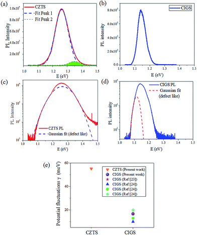
The performances of the CZTS and CIGS solar cells are listed in Table 1. The bandgap of the CZTS absorber is about 0.3 eV larger than the surface bandgap of the CIGS absorber, while the Voc of the CZTS solar cell is about 90 mV lower than that of the CIGS solar cell. To study the Voc deficiency problem in the CZTS solar cell, PL, AS and DLCP were employed to identify the different defect properties of the CZTS and CIGS solar cells. Fig. 1(a) shows the room temperature PL spectra of the CZTS and CIGS solar cells. The PL peaks of both solar cells are shifted to lower energies with respect to their bandgap energy Eg. However, the red shift of the PL peak relative to Eg for CIGS solar cell is relatively small (<5 meV) compared to that of the CZTS solar cell, which has a pronounced shift (∼190 meV). In addition, the CZTS PL spectrum has a larger FWHM than that of the CIGS PL spectrum. Eg − qVoc, the difference between the bandgap and qVoc is plotted in Fig. 1(b). The CZTS solar cell has a larger Voc deficit than that of the CIGS solar cell. This large Voc deficiency in the CZTS in Fig. 1(b) is consistent with the pronounced red shift of the PL peak relative to Eg for CZTS device in Fig. 1(a). As indicated in the literature, a large red shift of the PL peak relative to Eg and the broadening of PL peaks can be often attributed to the potential fluctuations in CZTS absorber layers.13,20,21 The tail states introduced by the potential fluctuation will reduce the effective bandgap of the absorber and thus decrease the Voc of solar cells. To get more detailed information on the potential fluctuation, we have performed low temperature PL measurement since the carriers are intended to be trapped at those tail states when temperature is low. Fig. 2(a) shows the PL spectrum of the CZTS solar cell at 10 K. Compared to the PL spectrum measured at room temperature (Fig. 1(a)), the peak measured at 10 K shifts to lower energy. Two peaks located at 1.25 eV and 1.35 eV, respectively, are observed. Emission at lower energy can be attributed to carriers in localized states while the high energy emission involves states that are delocalized.18 To estimate the potential fluctuation, we use the models developed by S. Siebentritt et al.,16 in which the low-energy tail of the PL band due to fluctuations is treated either as defects (justified for deep enough fluctuations), and the density of states assumes a Gaussian shape, or treated as Urbach tails, and the density of states shows an exponential decay.15,16| I(E) ∼ exp(−E/γ) or I(E) ∼ exp(−(E − E0)2/2γ2) | (1) |
| Sample | Bandgap (eV) | Voc (mV) | Jsc (mA cm−2) | FF (%) | η (%) |
|---|---|---|---|---|---|
| CZTS | 1.510 | 623 | 15.7 | 63.9 | 6.25 |
| CIGS | 1.220 | 715 | 35.0 | 77.7 | 19.4 |
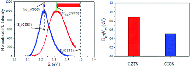 | ||
| Fig. 1 (a) Room temperature PL spectroscopy of CZTS and CIGS. (b) Voc deficiency compared to bandgap in CZTS and CIGS. | ||
To study the transition mechanism in solar cells, excitation density and temperature dependent PL spectroscopy were performed. As shown in Fig. 3(a), PL intensity increases with the excitation laser power. These intensities have been fitted in Fig. 3(b) using the power law:
| I ∝ Pk | (2) |
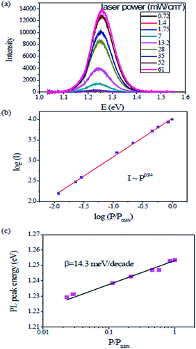 | ||
| Fig. 3 (a) Power dependent PL spectroscopy of CZTS at 10 K. (b) Power law fitting with coefficient of 0.94 ± 0.01. (c) Peak shift as a function of laser power. | ||
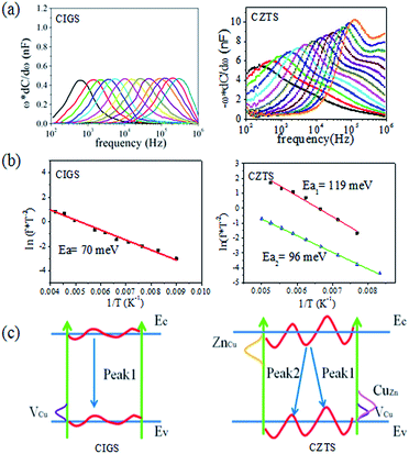
To further compare the bulk defect density and interface defect density in CZTS and CIGS solar cells, CV and DLCP measurements were used.15 Since DLCP is insensitive to the response from the interface or near-interface states, we can extract the contribution of the interface states by subtracting the DLCP defect density from the CV defect density. In addition, since the defects cannot respond effectively to the excitation signals at high frequencies, the detected DLCP signal hence provides us the information of free carrier concentration. The measured CV and DLCP of CIGS device at different frequencies are shown in Fig. 5(a). By analyzing the CV and DLCP results, we presented both the bulk trap density and interface defect density in CZTS and CIGS for comparison. Detailed defect density and free carrier density are listed in Table 3. For CZTS, same to previous publication,32 both the bulk defect density and interface defect density are two orders higher than those in the CIGS solar cell. The higher bulk defect density of CuZn and ZnCu with deeper defect level in the CZTS sample will cause larger potential fluctuations, which is also consistent with the PL measurement result. From Table 3, we can find that the interface states density in CZTS is also much higher. There are two possible reasons which can explain the higher interface defect density as observed in the CZTS cell. Firstly, the large lattice misfit between CZTS and CdS (about 7%) may result in interface dislocation/defects and cause minority carrier recombination at the CdS/CZTS interface.34,35 Secondly, when “cliff-like” band alignment occurs at the CdS/CZTS interface as shown in Fig. 5(c), it is equivalent to an interface bandgap reduction which will enhance the recombination, especially for the recombination between electrons in the conduction band of the buffer and holes in the valence band. Due to the high recombination at the CZTS/CdS interface, the Voc of the device will significantly decrease.34,36 However, we have to say that the formation of “cliff-like” or “spike-like” heterojunction between CdS and CZTS is still an open question.31,35,37,38
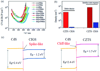 | ||
| Fig. 5 (a) DLCP of CIGS solar cell (measured at 170 K) (DLCP of CZTS solar cell not shown here, refer to ref. 32). (b) Defect and interface density of CZTS and CIGS. (c) Schema of the band alignment of CdS/CZTS and CdS/CIGS. | ||
| Sample | Nt (cm−3) | Ni (cm−3) | Nf (cm−3) |
|---|---|---|---|
| a Nt: bulk defect density, Ni: interface defect density, Nf: free carrier density. | |||
| CZTS | 1.0 × 10¹⁶ | 4.0 × 10¹⁶ | 1.0 × 10¹⁶ |
| CIGS | 1.3 × 10¹⁴ | 5.6 × 10¹⁴ | 3.2 × 10¹⁴ |
Based on the above findings, we may conclude that the large Voc deficit which limits the efficiency of the CZTS solar cells is related to both the larger potential fluctuations and higher density interface defects by comparing with CIGS. The potential fluctuation in CZTS is caused by both donors of ZnCu and acceptors of CuZn which have deeper ionization level and much higher population than those of the dominant defect VCu in CIGS. To make CZTS device be with efficiency comparable to CIGS, one has to pay more attention on the defects in the absorber. In addition to optimize the growth parameters to reduce the defect density, it will be with great help to reduce the potential fluctuation if the deep acceptor CuZn can be partly replaced by shallow acceptor VCu. Since the electrons in CZTS also experiences strong localization due to the potential fluctuation introduced by the donors, a design of graded conduction band similar to CIGS will benefit the transport of electrons and thus increase the device efficiency. Band engineering using spatial variation of Se/(S + Se) or Sn/(Ge + Sn) in Cu2ZnSn(S,Se)4 or Cu2Zn(Sn,Ge)Se4 will take the advantage of Ga/(Ga + In) grading in CIGS to facilitate the efficient collection of photo-generated electrons.
4. Conclusions
In this work, PL spectroscopy, DLCP, and AS measurement were used to characterize the factors limiting the performance of the CZTS solar cell by comparing with CIGS. Our results suggest that deep defect energy of acceptor CuZn and donor ZnCu, and resulting large potential fluctuation of the band structure, together with high density of interface defects cause the limitation of the efficiency of CZTS solar cell. The potential fluctuation in CIGS comes mainly from the dominant shallow acceptor VCu. Optimizing the growth parameters to suppress the deep CuZn defect and to increase the advantageous VCu will possibly reduce the resulting potential fluctuation. To overcome the potential fluctuation induced trapping effect for electrons by the ZnCu donors, we suggest that a graded conduction band similar to CIGS will be a good solution to eliminate electron localization.Acknowledgements
This work is supported by 973 project of China under 2012CB933700, NSF of China under 61274093 and 51302304, 51302303. We will also thank ITC funding of Shen Zhen under projects KQC201109050091A and JCYJ20120617151835515.Notes and references
- Y. B. K. Kumar, G. S. Babu, P. U. Bhaskar and V. S. Raja, Sol. Energy Mater. Sol. Cells, 2009, 93, 1230–1237 CrossRef PubMed.
- D. B. Mitzi, O. Gunawan, T. K. Todorov, K. Wang and S. Guha, Sol. Energy Mater. Sol. Cells, 2011, 95, 1421–1436 CrossRef CAS PubMed.
- N. Yu, R. Z. Zhong, W. J. Zhong, X. L. Chen, J. Luo, X. D. Gu, X. H. Hu, L. S. Zhang, J. Q. Hu and Z. G. Chen, RSC Adv., 2014, 4, 36046–36052 RSC.
- K. Ito and T. Nakazawa, Jpn. J. Appl. Phys., 1988, 27, 2094–2097 CrossRef CAS.
- K. Jimbo, R. Kimura, T. Kamimura, S. Yamada, W. S. Maw, H. Araki, K. Oishi and H. Katagiri, Thin Solid Films, 2007, 515, 5997–5999 CrossRef CAS PubMed.
- H. Katagiri, K. Jimbo, S. Yamada, T. Kamimura, W. S. Maw, T. Fukano, T. Ito and T. Motohiro, Appl. Phys. Express, 2008, 1, 41201 CrossRef.
- A. Ennaoui, M. Lux-Steiner, A. Weber, D. Abou-Ras, I. Kötschau, H.-W. Schock, R. Schurr, A. Hölzing, S. Jost, R. Hock, T. Voß, J. Schulze and A. Kirbs, Thin Solid Films, 2009, 517, 2511–2514 CrossRef CAS PubMed.
- J. Madarász, P. Bombicz, M. Okuya and S. Kaneko, Solid State Ionics, 2001, 141–142, 439–446 CrossRef.
- T. Todorov, O. Gunawan, S. J. Chey, T. G. Monsabert, A. Prabhakar and D. B. Mitzi, Thin Solid Films, 2011, 519, 7378–7381 CrossRef CAS PubMed.
- W. Wang, M. T. Winkler, O. Guanwa, T. Gokmen, T. K. Godorov, Y. Zhu and D. B. Mizi, Adv. Energy Mater., 2014, 4, 1301465 Search PubMed.
- T. Kato, H. Hiroi, N. Sakai, S. Muraoka and H. Sugimoto, 27th European Photovoltaic Solar Energy Conference, 2012, DOI:10.4229/27thEUPVSEC2012-3CO.4.2.
- ZSW press release, Stuttgart, September 22, 2014.
- T. Gokmen, O. Gunawan, T. K. Todorov and D. B. Mitzi, Appl. Phys. Lett., 2013, 103, 103506 CrossRef PubMed.
- K. Tanaka, T. Shinji and H. Uchiki, Sol. Energy Mater. Sol. Cells, 2014, 126, 143–148 CrossRef CAS PubMed.
- E. O. Kane, Phys. Rev., 1963, 131, 79–88 CrossRef.
- S. Siebentritta, N. Papathanasioua and M. C. Lux-Steine, Phys. B, 2006, 376–377, 831–833 CrossRef PubMed.
- J. H. Werner, J. Mattheis and U. Rau, Thin Solid Films, 2005, 480–481, 399–409 CrossRef CAS PubMed.
- T. Gershon, B. Shin, T. Gokmen, S. Lu, N. Bojarczuk and S. Guha, Appl. Phys. Lett., 2013, 103, 193903 CrossRef PubMed.
- J. T. Heath, J. D. Cohen and W. N. Shafarman, J. Appl. Phys., 2004, 95, 1000–1010 CrossRef CAS PubMed.
- J. Mattheis, U. Rau and J. H. Werner, J. Appl. Phys., 2007, 101, 113519 CrossRef PubMed.
- D. P. Halliday, R. Claridge, M. C. J. Goodman, B. G. Mendis, K. Durose and J. D. Major, J. Appl. Phys., 2013, 113, 223503 CrossRef PubMed.
- J. Krustok, J. Raudoja, M. Yakushev, R. D. Pilkington and H. Collan, Phys. Status Solidi, 1999, 173, 483–490 CrossRef CAS.
- J. Krustok, H. Collan, M. Yakushev and K. Hjelt, Phys. Scr., 1999, 79, 179–182 CrossRef.
- I. Dirnstorfer, M. Wagner, D. M. Hofmann, M. D. Lampert, F. Karg and B. K. Meyer, Phys. Stat. Sol., 1998, 168, 163–175 CrossRef CAS.
- M. Grossberg, J. Krustok, A. Jagomägi, M. Leon, E. Arushanov, A. Nateprov and I. Bodnar, Thin Solid Films, 2007, 515, 6204–6207 CrossRef CAS PubMed.
- J. P. Leitão, N. M. Santos, P. A. Fernandes, P. M. P. Salomé, A. F. da Cunha, J. C. González, G. M. Ribeiro and F. M. Matinaga, Phys. Rev. B, 2011, 84, 024120 CrossRef.
- K. Tanaka, Y. Miyamoto, H. Uchiki, K. Nakazawa and H. Araki, Phys. Stat. Sol., 2006, 203, 2891–2896 CrossRef CAS PubMed.
- L. Van Puyvelde, J. Lauwaert, P. F. Smet, S. Khelifi, T. Ericson, J. J. Scragg, D. Poelman, R. Van Deun, C. Platzer-Björkman and H. Vrielinck, Thin Solid Films, 2015, 582, 146–150 CrossRef CAS PubMed.
- M. Grossberg, P. Salu, J. Raudoja and J. Krustok, J. Photonics Energy, 2013, 3, 030599 CrossRef PubMed.
- S. Y. Chen, A. Walsh, X. G. Gong and S. H. Wei, Adv. Mater., 2013, 25, 1522–1539 CrossRef CAS PubMed.
- S. Y. Chen, J. H. Yang, X. G. Gong, A. Walsh and S. H. Wei, Phys. Rev. B, 2010, 81, 245204 CrossRef.
- G. M. Cheng, Y. Feng, Z. H. Li, L. Yin, X. D. Xiao and C. L. Yang. Defect study of CZTS solar cells by admittance spectroscopy, submitted.
- A. Walsh, S. Y. Chen, S. H. Wei and X. G. Gong, Adv. Energy Mater., 2012, 2, 400–409 CrossRef CAS PubMed.
- W. Li, J. Chen, C. Yan and X. J. Hao, J. Alloys Compd., 2015, 632, 178–184 CrossRef CAS PubMed.
- A. Nagoya, R. Asahi and G. Kresse, J. Phys.: Condens. Matter, 2011, 23, 404203 CrossRef CAS PubMed.
- T. Minemoto, T. Matsui, H. Takakura, Y. Hamakawa, T. Negami, Y. Hashimoto, T. Uenoyama and M. Kitagawa, Sol. Energy Mater. Sol. Cells, 2001, 67, 83–88 CrossRef CAS.
- M. Bar, B. A. Schubert, B. Marsen, R. G. Wilks, S. Pookpanratana, M. Blum, S. Krause, T. Unold, W. Yang, L. Weinhardt, C. Heske and H. W. Schock, Appl. Phys. Lett., 2011, 99, 222105 CrossRef PubMed.
- R. Haight, A. Barkhouse, O. Gunawan, B. Shin, M. Copel, M. Hopstaken and D. B. Mitzi, Appl. Phys. Lett., 2011, 98, 253502 CrossRef PubMed.
| This journal is © The Royal Society of Chemistry 2015 |

