
Ohmic contact of indium oxide as transparent electrode to n-type indium phosphide
Xiufeng Tang*ab,
Chunhan Hseiha,
Fang Oua and
Seng-Tiong Hoa
aDepartment of Electrical Engineering and Computer Science, Northwestern University, Evanston, Illinois 60208, USA. E-mail: tbrenda@sina.com; chunhanhseih2013@u.northwestern.edu; sth@northwestern.edu; Tel: +86 029 88494574
bState Key Laboratory of Solidification Processing, School of Materials Science and Engineering, Northwestern Polytechnical University, Xi'an 710072, China
First published on 23rd February 2015
Abstract
Ohmic contacts of n-type indium phosphide (n-InP) with indium oxide (In2O3), a transparent conducting oxide (TCO), have been achieved. Hydrogen plasma surface pretreatment of the n-InP substrates (H2-cleaned n-InP) prior to the deposition of In2O3 films, is the key to achieve Ohmic contact. Oxygen flow rate during the In2O3 film deposition, which equivalently determines its doping level, is the main tuning parameter for In2O3 thin films growth. Rapid thermal annealing process (RTP) at different temperatures was found to have little effects on the Ohmic contact type.
1. Introduction
Transparent high-conductivity Ohmic contacts are of primary importance for optoelectronic devices, such as high electron mobility transistors,1 light emitting diodes (LEDs)2 and solar cells.3 Although the large band gaps usually associated with optical transparency preclude the possibility of high conductivity in many transparent materials, a number of metal oxides, known as transparent conducting oxides (TCOs), possess the unique properties of being both transparent and highly conductive.4Compared with the majority of TCOs, indium oxide (IO) as a binary compound TCO does not need extrinsic doping and has the advantage of ease of tuning the chemical composition during film deposition. What's more, the superiority of IO films over tin oxide (SnO2) films as transparent electrodes is largely due to the higher mobility in IO.5 IO films prepared by various techniques have mobility in the range of 10–75 cm2 V−1 s−1, with carrier concentration around 1019–1020 cm−3.5 The optical transmittance of IO films in the visible and near-IR regions is about 75–90%.6–8 Additionally, the refractive index of IO films in the visible region ranges between 1.9 and 2.08.8,9 The low refractive index of IO relative to InP (n ≈ 3.2) also possesses the possibility that IO could be used as a conducting waveguide cladding material for current injection into high refractive index contrast nanophotonic devices.10,11 A critical concern for these applications, however, is the electrical properties across the interface between the IO films and InP substrates. The contact should be Ohmic and the resistance should be minimized.12,13
Generally, in order to achieve Ohmic contact between a TCO film and an n-type nondegenerate semiconductor, it is required that the Fermi level of the TCO (øIO) be less than that of the semiconductor (øInP).14,15 For the donor-doped n-InP substrates used in this study (n = 7.00 × 1017 cm−3), the Fermi level (EF) is estimated to be 0.39 eV below the conduction band minimum (Ec) by using eqn (1), shown as follows,
 | (1) |
In this paper, we present results for optical and electrical properties of indium oxide (In2O3) thin films deposited by ion beam assisted deposition (IAD). The electrical contact properties across the interface between the contact material, In2O3, and the semiconductor, n-InP are investigated. The oxygen partial pressure during deposition is the main tuning parameter for In2O3 films growth. Effects of oxygen partial pressure during deposition on microstructure and surface morphology, grain size and surface roughness, optical and electrical properties of In2O3 films were ever systematically reported.24–26 While, in our study, In2O3 films will be used as cladding electrodes and therefore optical and electrical properties of bulk In2O3 films and especially the interfacial electrical contact properties are our big concern. In addition, we know, in InP based photonic device fabrication, rapid thermal annealing processes (RTP) are often required. So, it is also necessary to investigate what effect RTP would have on the interfacial contact properties between In2O3 and InP.
2. Experimental
2.1 Film preparation
In2O3 thin films were prepared at room temperature using Ion-Assisted Deposition (IAD, ION TECH, INC, USA) with In2O3 target (99.99% pure, Kurt J. Lesker company). IAD consists of a main ion source and an assisted ion source. The main beam will sputter out In2O3 from the target, while the assistant beam directed toward the substrate will provide additional kinetic energy to the sputtered In2O3, increasing the film surface energy without further heating. Therefore, thin films prepared by IAD possess good adhesiveness without additional substrate heating. In addition, cooling water running in the back of the sample further stabilizes the local temperature during deposition and does not exceed 50 °C.Properties of In2O3 are strongly dependent on its doping level, which are mainly oxygen vacancies. The oxygen partial pressure, which is controlled by the oxygen flow rate of the assistant beam during deposition, is therefore the main tuning parameter for In2O3 thin films growth. Oxygen flow rates of 0 sccm, 3 sccm, 5 sccm, and 7 sccm were used and the deposited corresponding thin films are referred to as In2O3-0, In2O3-3, In2O3-5, and In2O3-7 respectively. Deposition time is 60 min and the working pressure is 4.5 × 10⁻⁴ Torr. The film thickness is about 100 nm, which is tested by an alpha-step 200 from Tencor Instruments. Other detailed parameters of In2O3 deposition are listed in Table 1.
| Forward power (W) | Beam voltage (V) | Accelerate voltage (V) | Beam current (mA) | Argon neutron (sccm) | Argon source (sccm) | Oxygen (sccm) |
|---|---|---|---|---|---|---|
| Main beam | ||||||
| 200 | 1000 | 160 | 85 | 3 | 10 | 25 |
![[thin space (1/6-em)]](https://www.rsc.org/images/entities/char_2009.gif) |
||||||
| Assisted beam | ||||||
| 110 | 150 | 100 | 31 | 3 | 10 | 0, 3, 5, 7 |
2.2 Bulk In2O3 properties measurement
Bulk material properties of In2O3 were characterized using thin films deposited on commercial glass slides. Electrical properties were carried out using Hall Effect measurements with films of Van der Pauw geometry. For optical properties, transmittance and reflectance spectra were measured in the spectral range from 200 nm to 2000 nm using a UV/Vis/IR Perkin-Elmer lambda 1050 spectrophotometer with the integrating sphere in the dual beam mode. Microstructure of the as-deposited In2O3-3 film was examined using scanning electron microscope (SEM, Hitachi S4800) and an RIGAKU: ATX-G X-ray diffractometer.2.3 Contact patterns fabrication and electrical contact properties measurement
Interfacial properties are characterized using the In2O3 thin films deposited on n-type InP substrates (n = 7.00 × 1017 cm−3). Prior to deposition, all InP substrates were first solvent cleaned in 3 minutes of ultrasonic bath sequentially in acetone, IPA (Isopropyl Alcohol), and then deionized water; substrates cleaned by this method are referred to as solvent-cleaned samples. Some substrates were further cleaned by reactive ion etching (RIE) in oxygen and others in Hydrogen (O2 or H2, 50 mtorr, 100 W, 1 min). Samples received surface treatments of RIE plasma cleaning are referred to as O2-cleaned or H2-cleaned. It should be noted that all samples were directly put into IAD apparatus right after ex situ pretreatments. B. Anthony's study27 showed that H plasma clean can protect the wafer from contamination for up to 15 min in ambient air. So the elapse was shortened to be less than10 min.In order to examine the electrical contact properties, photolithography process was used to define contact patterns for transmission line method measurements. Fabrication process flow is shown in Fig. 1: linear arrays of 200 um by 200 um square pads with various gap distances apart (10–60 um gap in 10 um increment). Ti/Au (10 nm/300 nm) was then deposited by E-beam evaporation followed by a lift-off process to form metal contacts on In2O3. Finally, using the deposited metal pads as a self-alignment mask, the exposed In2O3 film was removed using RIE in Methane/H2/Ar gases (CH4:H2:Ar = 10:30:10 sccm, 50 mtorr, 200 W) to complete the fabrication process. The electrical current–voltage characteristics between In2O3 films and InP substrates were measured by standard two-probe measurement method using a Kiethley 2400 source meter.
 | ||
| Fig. 1 Schematic representation of the fabrication process used to define the electrical contact measurement pattern. | ||
2.4 Annealing heat treatments detail
The annealing treatments were carried out using a Jet First 100/150 Rapid Thermal Process, at 360 °C, 400 °C and 450 °C, which are the temperatures chosen for device contact annealing. The annealing duration is 60 seconds, while the temperature was raised rapidly in 10 seconds in forming gas (20% H2, balance N2).3. Results and discussion
3.1 Properties of bulk In2O3
The measured electrical and optical properties of bulk In2O3 are concisely summarized in Table 2. From Table 2, we can tell with increasing the O2 flow rate during the film deposition, the carrier concentration decreases from 8.53 × 10¹⁹ to 2 × 1017 cm−3. Higher oxygen partial pressure during film deposition results in lower carrier concentration due to the reduction of oxygen vacancies. The Hall mobility of In2O3 ranges from 13.1–29.3 cm2 V−1 s−1; the conductivity is highest at 355.5 S cm−1 for In2O3-0, while for In2O3-7 the conductivity is as small as 0.71 S cm−1, which indicates that In2O3-7 is highly oxidized and low in oxygen vacancies.| Deposition Condition (O2 flow rate) | 0 | 3 | 5 | 7 |
|---|---|---|---|---|
| Carrier Concentration (cm−3) | 8.53 × 10¹⁹ | 2.13 × 10¹⁹ | 2 × 10¹⁹ | 2 × 10¹⁷ |
| Conductivity (S cm−1) | 355.5 | 99.9 | 41.9 | 0.71 |
| Hall mobility (cm2 V−1 s−1) | 26.1 | 29.3 | 13.1 | 21.5 |
| Complex Refr. Ind.@1550 nm (n + ik) | 1.84 + 0.025i | 1.952 + 0.0102i | 1.9662 + 0.0071i | 2.01 + 0.004i |
| Optical loss@ 1550 nm (cm−1) | 2061.8 | 831.1 | 571.9 | 320.7 |
| Optical band gap (eV) | 3.75 | 3.7 | 3.68 | 3.65 |
We know that fiber-optic communication transmission windows around 1500 nm are most widely-used, which have the lowest attenuation losses and achieve the longest range. Therefore, in this study, the optical constants (refractive index n and absorption coefficient k) at 1550 nm are extracted from the transmittance and reflectance spectra, shown in Fig. 2, corrected by the substrate transmittance and reflectance spectra employing the interference pattern resulted from multiple reflections in the film and the glass substrate. From Fig. 2, we know that the optical transmittance of In2O3 in the visible and near-IR regions is about 75–90%, which is consistent with reported data.6,7 The high optical transparency of In2O3 in the visible and near-IR regions is a direct consequence of its wide band gap (Eg ∼ 3.0 eV).28 Additionally, the fundamental absorption edges of In2O3 generally lie in the UV and shift to shorter wavelengths with lower O2 flow rate, due to the increasing carrier concentration. The refractive index in the visible region increases from 1.84 to 2.01 in dependence of the increasing O2 flow rate during the deposition, because of the more sufficient oxidation. Optical loss at 1550 nm is highest for In2O3-0 at 2061 cm−1 and lowest for In2O3-7 at 320.7 cm−1, where higher loss at higher carrier concentration results from free carrier absorption and free carrier scattering.
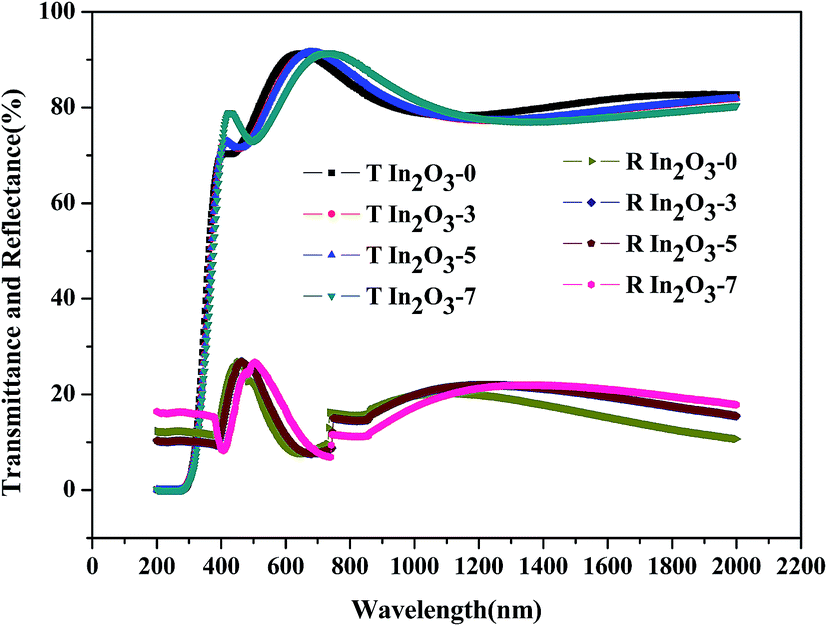 | ||
| Fig. 2 Transmittance and reflectance spectra of In2O3-0, In2O3-3, In2O3-5 and In2O3-7. | ||
The optical band gap of In2O3 is estimated using the graph of (αhν)2 versus hν29 (as shown in Fig. 3), where α, the optical attenuation coefficient at energy hν, is extracted from the transmittance and reflectance spectra using the relation α = −(1/d)log(T/(1 − R)), where d is the film thickness. From Fig. 3, we can tell the optical band gap increases with the increasing carrier concentration. The optical band gap energy depends on the carrier concentration as a result of the band filling effect, also known as the Burstein-Moss shift:30 the filling of excessive carrier in the conduction band leads to the increase of the optical band gap energy. To sum up, a trade-off relation is indicated for the engineering of the conductivity and the optical loss of bulk In2O3 thin films.
 | ||
| Fig. 3 Graph of (αhν)2 versus photon energy (eV). | ||
3.2 Microstructure of In2O3 films
SEM and XRD spectrum of the as-deposited In2O3-3 film was shown in Fig. 4. The SEM result shows that the as-deposited film prepared by IAD is smooth and dense with grain size about 50 nm. And the XRD result shows that the as-deposited film is already polycrystalline, but some amorphous contribution can not be excluded. Structures comprising amorphous and polycrystalline components are common for In2O3 films annealed or processed below 200 °C.31 Regarding In2O3, the film exhibits sharp crystalline peaks, which clearly correspond to the cubic structure of the mineral bixbyite (JCPDS 6-0416). For In2O3, deposited at low temperature, the predominant planes are (222) and (400),32 which is the case here. A (100) or (111) preferred orientation has generally been reported in In2O3 films which have been obtained by various techniques.8,33,34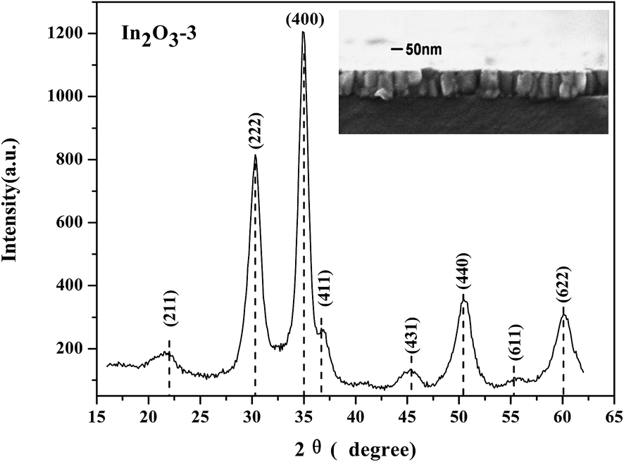 | ||
| Fig. 4 SEM and XRD spectra of the as-deposited In2O3-3 film. | ||
3.3 Interfacial electrical contact property
For interfacial electrical contact experiments, contacts to n-type InP substrates pretreated with standard solvent cleaning, O2 cleaning and H2 cleaning, from thin films of In2O3-0, In2O3-3, In2O3-5, and In2O3-7, were examined. Fig. 5 shows I–V curves of the In2O3 contact to n-InP of different O2 flow rates during In2O3 deposition: (a) solvent-cleaned n-InP substrates; (b) O2-cleaned n-InP substrates; (c) H2-cleaned n-InP substrates. For solvent-cleaned substrates as shown in Fig. 5(a), Ohmic contact is shown for n-InP to In2O3-0 and In2O3-3 thin films, while Schottky behavior is shown for In2O3-5, and In2O3-7 contacts to n-InP. The difference in carrier concentration results in different Fermi energy and work function of the In2O3 films, whereas the energy bands are predominately aligned for less oxidized, films with higher carrier concentration forming the Ohmic contact. However, for O2 plasma cleaned substrates, all film contacts to n-InP show Schottky behavior (seen in Fig. 5(b)). This implies that an interfacial oxide layer might exist between the film and the substrate for O2 plasma pretreated samples.23 If such oxide layer exists and causes the Schottky behavior, the removal of such layer could allow the formation of Ohmic contact. Then some substrates were treated by H2 plasma after standard solvent cleaning prior to In2O3 film deposition. The contact measurements of those samples are shown in Fig. 5(c). All In2O3 films form Ohmic contact to n-InP substrates pre-treated using H2 plasma. | ||
| Fig. 5 I–V curve measurements of the In2O3 contacts to n-InP of different O2 flow rates during film deposition: (a) solvent-cleaned n-InP substrates; (b) O2-cleaned n-InP substrates; (c) H2-cleaned n-InP substrates. | ||
Dynamic resistances of In2O3 film contacts to H2-cleaned InP substrates in terms of different O2 flow rates during film deposition are listed in Fig. 6, which are calculated from the I–V curves such as those in Fig. 5(c). It can be seen that the dynamic resistance shows a decreasing trend with the increasing O2 flow rate. It should be noted that besides the In2O3 film resistance and the In2O3/InP contact resistance, the dynamic resistance as calculated from I–V curves is the total resistance also including the resistances due to the probes, the metal pads, the InP substrate, and the probe/metal and the metal/In2O3 interfaces but these resistances are not affected by the increasing O2 flow rate and the hydrogen pretreatment. In consideration of the decreasing conductivity of the In2O3 films with the increasing O2 flow rate, seen in Table 2, we can conclude that the dynamic In2O3/InP interfacial contact resistance decreases with tuning the O2 flow rate from 0 sccm to 7 sccm, after hydrogen pretreatment. On the other hand, comparing with the dynamic resistances of In2O3-0 and In2O3-3 films contacts to solvent-cleaned InP substrates calculated from Fig. 5(a) as 2.46 Ω and 2.78 Ω separately, the dynamic resistances of those films contacts to H2-cleaned InP substrates are 2.12 Ω and 2.07 Ω separately, as shown in Fig. 6. It means that the hydrogen plasma pretreatment is not only crucial for In2O3 films to form Ohmic contact with n-InP substrates but also good for improving the interfacial conductivity of the In2O3/InP contact.
 | ||
| Fig. 6 Dynamic resistances of In2O3 film contacts to H2-cleaned n-InP substrates in terms of different O2 flow rates. | ||
Fig. 7(a) shows the I–V curve measurements of the In2O3-3 contacts to H2-pretreated n-InP substrates in terms of different post-deposition rapid thermal processes (RTP) to investigate whether the annealing process will affect the ohmic contact property. It can be seen that the contact properties between In2O3 and n-InP remain to be Ohmic after all the annealing heat treatments at 360 °C, 400 °C and 450 °C. This might be due to the carrier concentration remains unchanged (mainly oxygen vacancies). Meanwhile, the dynamic resistance of the In2O3-3 film/n-InP substrate samples were calculated, as plotted in Fig. 7(b). Comparing with that of the as-deposited sample at 2.07 Ω, the dynamic resistance first increases slowly to 2.3 Ω when the annealing temperature is lower than 400 °C and then increases sharply to 3.3 Ω with the temperature increased to 450 °C. Effects of annealing heat treatments at various temperatures, in different atmosphere or for different duration time on electrical properties of In2O3 films were ever investigated.35–37 Especially, Yuan's study of annealing on In2O3 films in vacumm,35 Oh's study of annealing on Al-doped ZnO films in H2 atmophere38 and Lin's study of annealing on In2O3:Sn films in N2 atmosphere39 have shown that grain size will increase and crystallite quality will be promoted after annealing process and the resistivity of bulk films will decrease, either due to the grain boundary scattering mechanism35 or originating from the desorption of the negatively charged oxygen species from the grain boundary surfaces by the hydrogen treatment.38 So resistivity of bulk In2O3 films will get lower after annealed in H2 + N2 atmosphere. What is more, besides the bulk In2O3 film resistance and the In2O3/InP contact resistance, the dynamic resistance includes resistance due to the probes, the metal pads, the InP substrate, and the probe/metal and the metal/In2O3 interfaces that remains as a constant. Therefore, we can conclude that the In2O3/InP interfacial contact resistances first increase slowly with the increasing annealing temperature and then change sharply when the annealing temperature is high at 450 °C, which can be probably explained by the interfacial diffusion.
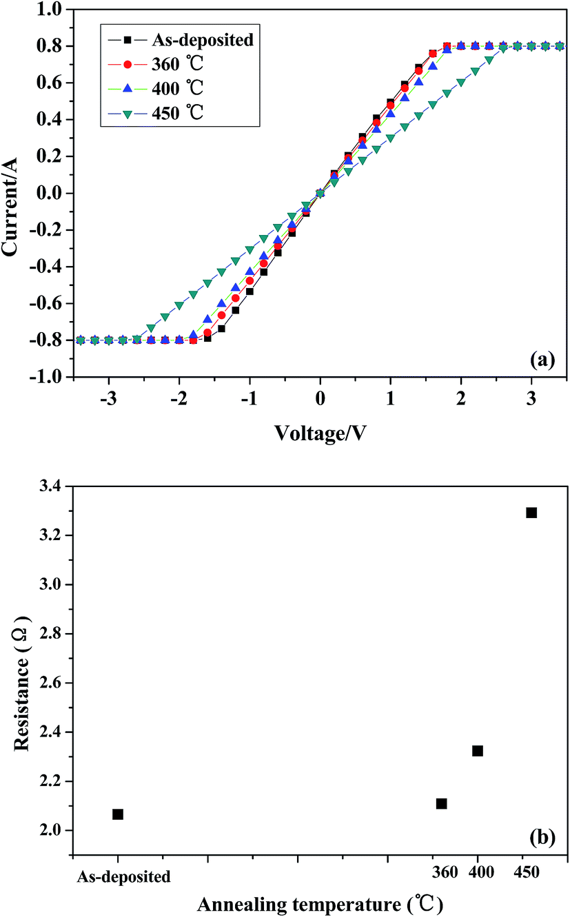 | ||
| Fig. 7 In2O3-3 contacts to H2-cleaned n-InP substrates in terms of different post-deposition annealing temperatures, (a) I–V curve measurements; (b) calculated dynamic resistances. | ||
All results show that though the Ohmic contact of In2O3 to n-InP is not only compatible to RTP but also the RTP is good for improving the quality of In2O3 films, the conductivity of the In2O3/InP contacts will deteriorate drastically when the annealing temperature is too high, suggesting that choosing optimal annealing temperature is important in device contact heat treatments.
4. Conclusions
Ohmic contact of In2O3 thin films prepared by IAD to n-type InP can be achieved with H2 plasma pre-treated substrates, which isn't obviously affected by tuning the oxygen flow rate during the film deposition or the post-deposition rapid thermal annealing processes. For optical and electrical properties, by tuning the ambient oxygen pressure during the film deposition, we obtained In2O3 films with low optical loss (lowest at 320.7 cm−1 for In2O3-7) at the 1550 nm wavelength range and reasonable conductivity (highest at 355.5 S cm−1 for In2O3-0). These results indicate the promising potential of In2O3 thin films as transparent electrodes for designing InP based optoelectronic devices for optical communication applications.Acknowledgements
This work was partially made possible through financial support from the Northwestern IGERT fellowship grant. Use of the Center for Nanoscale Materials clean room of Argonne National Lab was supported under proposal number CNM30847.References
- D. Dawson, L. Samoska and A. K. Fung, et al., IEEE Microw. Wireless. Compon. Lett., 2005, 15, 874–876 CrossRef.
- Y. J. Liu, C. H. Yen and C. H. Hsu, et al., Opt. Rev., 2009, 16, 575–577 CrossRef CAS PubMed.
- J. Van de Lagemaat, N. G. Park and A. J. Frank, J. Phys. Chem. B, 2000, 104, 2044–2052 CrossRef CAS.
- T. Minami, New n-Type Transparent Conducting Oxides, MRS Bull., 2000, 38–44 CrossRef CAS.
- K. L. Chopra, S. Major and D. K. Pandya, Thin Solid Films, 1983, 102, 1–46 CrossRef CAS.
- S. Noguchi and H. Sakata, J. Phys. D: Appl. Phys., 1980, 13, 1129 CrossRef CAS.
- C. A. Pan and T. P. Ma, Appl. Phys. Lett., 1980, 37, 163 CrossRef CAS PubMed.
- C. E. Wickersham and J. Greene, Phys. Status Solidi A, 1978, 47, 329 CrossRef CAS.
- H. K. Muller, Phys. Status Solidi, 1968, 27, 723 CrossRef.
- N. Nunoya, M. Nakamura, M. Morshed, S. Tamura and S. Arai, IEEE J. Sel. Top. Quantum Electron., 2001, 7, 249–258 CrossRef CAS.
- T. Minami, Semicond. Sci. Technol., 2005, 20, S35–S44 CrossRef CAS.
- K. J. Chen, T. Enoki, K. Maezawa, K. Arai and M. Yamamoto, IEEE Trans. Electron Devices, 1996, 43, 252–257 CrossRef CAS.
- H. C. Lin, S. Senanayake, K. Y. Cheng and M. Hong, et al., IEEE Trans. Electron Devices, 2003, 50, 880–885 CrossRef CAS.
- T. V. Blank and Y. A. Gol’dberg, Semiconductors, 2007, 41, 1281–1308 CrossRef.
- S. Wang, Fundamentals of Semiconductor Theory and Device Physics, Prentice Hall, Upper Saddle River, NJ, 1989 Search PubMed.
- Physical Properties of Semiconductors, Ioffe Physico-Technical Institute, http://www.ioffe.ru/SVA/NSM/Semicond/index.html.
- D. S. GinleyH. Hosono and D. C. Paine, Handbook of Transparent conductors, Springer, New York, 2011, p. 160 Search PubMed.
- V. Korobov, M. Leibovitch and Y. Shapira, J. Appl. Phys., 1993, 74, 3251–3256 CrossRef CAS PubMed.
- A. Golan, J. Bregman, Y. Shapira and M. Eizenberg, Appl. Phys. Lett., 1990, 57, 2205–2207 CrossRef CAS PubMed.
- C. Donley, D. Dunphy and D. Paine, et al., Langmuir, 2002, 18, 450–457 CrossRef CAS.
- F. J. Milliron, I. G. Hill, C. Shen, A. Kahn and J. J. Schwartz, Appl. Phys., 2000, 87, 572–576 Search PubMed.
- C. C. Wu, C. I. Wu, J. C. Sturm and A. Kahn, Appl. Phys. Lett., 1997, 70, 1348–1350 CrossRef CAS PubMed.
- F. Ou, D. Bruce Buchholz and F. Yi, et al., ACS Appl. Mater. Interfaces, 2011, 3, 1341–1345 CAS.
- A. Golan, J. Bregman, Y. Shapira and M. Eizenberg, Appl. Phys. Lett., 1990, 57, 2205–2207 CrossRef CAS PubMed.
- V. Korobov, Y. Shapira, B. Ber, K. Faleev and D. Zushinskiy, J. Appl. Phys., 1994, 75(4), 2264–2269 CrossRef CAS PubMed.
- S. Karthikeyan, A. E. Hill and R. D. Pilkington, Thin Solid Films, 2014, 550, 140–144 CrossRef CAS PubMed.
- B. Anthony, T. Hsu, L. Breaux, R. Qian, S. Banerjee and A. Tasch, J. Electron. Mater., 1990, 19(10), 1027–1032 CrossRef CAS.
- J. Wu, W.-Q. Han, A. Janotti, H.-C. Kim, Functional Metal Oxide Nanostructures, Materials Research Society, 2009, p. 136 Search PubMed.
- P. Prathap, Y. P. V. Subbaiah, M. Devika and K. T. Ramakrishna Reddy, Mater. Chem. Phys., 2006, 100, 375–379 CrossRef CAS PubMed.
- E. Burstein, Phys. Rev., 1954, 93, 632 CrossRef CAS.
- P. Barquinha, R. Martins, L. Pereira, E. Fortunato, Transparent Oxide Electronics: From Materials to Devices, Wiley, 2012, p.19 Search PubMed.
- J. F. Wager, D. A. Keszler and R. E. Presley, Transparent Electronics, Springer, New York, 2008 Search PubMed.
- P. Nath, R. F. Bunshah, B. M. Basol and O. M. Staffsud, Thin Solid Films, 1980, 72, 463 CrossRef CAS.
- V. M. Vainshtein and V. I. Fistul, Sov. Phys. Semiconduct., 1967, 1, 104 Search PubMed.
- Z. Yuan, X. Zhu and X. Wang, et al., Thin Solid Films, 2011, 519, 3254–3258 CrossRef CAS PubMed.
- K. Kato, H. Omoto, T. Tomioka and A. Takamatsu, Thin Solid Films, 2011, 520, 110–116 CrossRef CAS PubMed.
- T. Suzuki, T. Yamazaki, M. Takizawa and O. Kawasaki, J. Mater. Sci., 1989, 24, 187–191 CrossRef CAS.
- B.-Y. Oh, M.-C. Jeong and D.-S. Kim, et al., J. Cryst. Growth, 2005, 281, 475–480 CrossRef CAS PubMed.
- L. Lin, F. Lai and Y. Qu, et al., Mater. Sci. Eng. B, 2007, 138, 166–171 CrossRef CAS PubMed.
| This journal is © The Royal Society of Chemistry 2015 |