
 Open Access Article
 This Open Access Article is licensed under a Creative Commons Attribution-Non Commercial 3.0 Unported Licence
From 1D to 3D: a new route to fabricate tridimensional structures via photo-generation of silver networks†
Huaizhong
Shen
a,
Yuxin
Wu
a,
Liping
Fang
a,
Shunsheng
Ye
a,
Zhaoyi
Wang
a,
Wendong
Liu
a,
Zhongkai
Cheng
a,
Junhu
Zhang
a,
Zhanhua
Wang
*b and
Bai
Yang
*a
aState Key Laboratory of Supramolecular Structure and Materials, College of Chemistry, Jilin University, Changchun, 130012, P. R. China. E-mail: byangchem@jlu.edu.cn
bLaboratory of Organic Chemistry, Wageningen University and Research Center, Dreijenplein 8, 6703 HB, Wageningen, The Netherlands. E-mail: wzh12020915@gmail.com
First published on 13th March 2015
Abstract
A rapid and cost effective method has been developed to fabricate 3 dimensional (3D) ordered structures by photo-generating silver networks inside a 1D layered heterogeneous laminate composed of poly(vinyl alcohol) (PVA) and poly(methyl methacrylate) (PMMA). By designing the photo-mask meticulously, the silver nanoparticles (NPs) produced by UV light aggregate to form frameworks in different forms, which perform as the anisotropic component, i.e. the building blocks, thus converting the 1D structure into 3D. Formation of silver NPs increases the refractive index (RI) of the PVA layers, thus bringing optical change to the 1D laminar structure, which allows us to trace the silver formation process by measuring the change of RI value and reflectance spectra. The 1D layered structure is a good building matrix for 3D construction because the total number of layers and the layer thickness can be finely tuned flexibly which allow us to further study the various properties caused by the structural modulation. By utilizing photo-reactive silver ions, an innovative strategy of fabricating 3D structures through in situ photo-generating silver building blocks inside the laminar matrix is established, which makes it possible to fabricate 3D micro/nano composite materials with potential applications in fields such as sensors and photonic meta-materials.
Introduction
Inspired by the typical structures existing in natural creatures,1–5 three dimensional ordered structures, of which the constituent component is orderly distributed in three dimensions, have drawn much attention from researchers due to their special applications in manipulating light propagation6 and cell differentiation7 and potential use in meta-materials.8,9 3D structures consisting of self-assembled colloidal spheres exhibit vivid and bright structural color10 which is derived from interference effects within their periodic distribution of building blocks, while 3D structure containing unit cells, which are much smaller than the wavelength of light, present many new and unusual optical properties.8 As the structures evolve, many new properties and applications are discovered and studied. Thus, constructing 3D structures with different forms is highly required.High resolution top-down approaches as well as bottom-up technologies have been developed to construct 3D structures on multiple scales, including electron-beam lithography,11 ion beam lithography,12 direct laser writing13 and self-assembly.14–18 For instance, researchers have successfully fabricated various 3D patterns and networks to be used as cell guidance scaffolds,19 tissue engineering matrices20 and in biomimetic manufacturing.21 Another category of 3D structures of great importance is the photonic meta-materials, which are man-made structures consisting of repeating periodic micro- or nanostructured metallodielectric building blocks. Since their first introduction around one decade ago,22 photonic meta-materials have been on a fast evolution to become smaller and more delicate.23,24 By precisely designing the patterns’ shape, geometry, size, orientation and arrangement ahead of fabrication and combining sophisticated top-down manufacture processes, the photonic meta-materials possess novel electromagnetic properties such as negative refractive index, perfect absorption and negative magnetic permeability, which do not exist in nature.25 There are also previous reviews summarizing the fabrication methods of meta-materials.26–30 Among them, the layer deposition technique, which involves pattern making in a single layer and a subsequent stacking process, is widely used to fabricate stacked 3D meta-materials. However, there remain challenges in the construction of such 3D structures.31 One is the repeated stacking of unit cells to qualify the structure as a real material, the other is to realize various styles of building blocks which has an obvious influence on the structure’s magnetic resonance frequency. In addition, the sophisticated technology and equipment involved in the fabrication process also increases the complexity and the cost. Hence, to exploit an easy and economical way to fabricate 3D ordered structures is of great importance.
From the above-mentioned applications we noticed one thing, that in the cases of both biological and photonic regulation, the 3D structures involve repeating patterned layer stacks, which are most likely a post-processed 1D layered structure. This suggests to us whether we can fabricate a 1D heterogeneous layered structure at the first step, then convert it into 3D through post-processing, such as a chemical reaction inside the layer stack. Based on the analysis above, polymeric 1D layers and metal ion–containing polymer films enter our field of vision. Previous studies prove that the light-induced reduction of metal ions embedded in polymer films is effective and well-conducted.32–34 Among them, the in situ reduction of silver ions has been studied extensively by scientists for its mild reactive chemistry in the solid phase.35,36 Mills and coworkers developed a method to produce silver nanoparticles (NPs) and clusters in crosslinked PVA/PAA films.37 The Ozin group incorporated silver NPs into the TiO2/clay layers to modify the photonic properties.38 Nesbitt et al. further studied the experimental protocol, reaction process and morphology of photo-generated Ag NPs.39 In addition, silver ions embedded in polymer films can be selectively reduced to aggregate into different 2D and 3D structures, possibly through a combination with photo-masks or direct laser writing technology which provides a route for photo-patterning.40,41 Furthermore, Ag NPs presents high catalytic activity,42 anti-bacteria ability43 and other potential uses, such as in SERS for their characteristic surface plasmon resonance,44,45 which may bring new functions to the ordered structure. For the reasons we mentioned above, silver NPs can be utilized to form building blocks for 3D construction beginning with a 1D layer structure as a building matrix.
In this paper, we first fabricated a polymer heterogeneous 1D layered structure doped with silver ions. By selectively reducing Ag+ in specific parts of the 1D layered stacks, 3D networks of Ag were formed inside the structure, making it turn out to be a 3D construction based on heterogeneous polymer lamination, which is an exemplified combination of top-down and bottom-up fabrication. By increasing the refractive index (RI) of the PVA layer, silver NPs strongly modified the optical properties of the 1D stack with an obvious photonic band gap (PBG) within 3 bilayers, which provides us with a chance to trace the silver reduction process by measuring reflectance spectra and RI values of the composite film. Modulation of the structural parameters of the 1D matrix such as period and number of layers can be achieved, which further enables the fine adjustment of the 3D structure. Finite-Difference Time-Domain (FDTD) simulations were also conducted to confirm our results. Our method realizes the successful combinatorial construction of a 1D layered matrix and photo-generated silver building blocks to form a 3D ordered structure, which has possibilities for potential applications in bioassays, SERS matrices and photonic meta-materials.6–9
Results and discussion
Building of the 3D structure
The process of constructing the 3D ordered structure is illustrated in Fig. 1. Briefly, the 3D structure is fabricated by exposing the as-prepared Ag+ doped 1D heterogeneous layer stacks to UV irradiation with a pre-designed mask, a process in which the in situ photo-reduction of silver ions happens in a specific area inside the laminar structure, leading to the formation of composite 3D polymer–silver NPs hybrid materials. Compared to traditional fabrication methods of building stacked 3D materials, which may involve sophisticated instruments or complicated processes, our approach is to generate building blocks after the acquisition of a layered structure. The alignment of the building blocks belonging to different layers is achieved by the rectilinear propagation of UV light, which is guaranteed by carefully selecting an irradiation source matching the scale of the patterns to avoid diffraction. Unlike the layer deposition technique we mentioned above, this method omits time-consuming processes such as aligning marker making, lateral aligning and planarization.46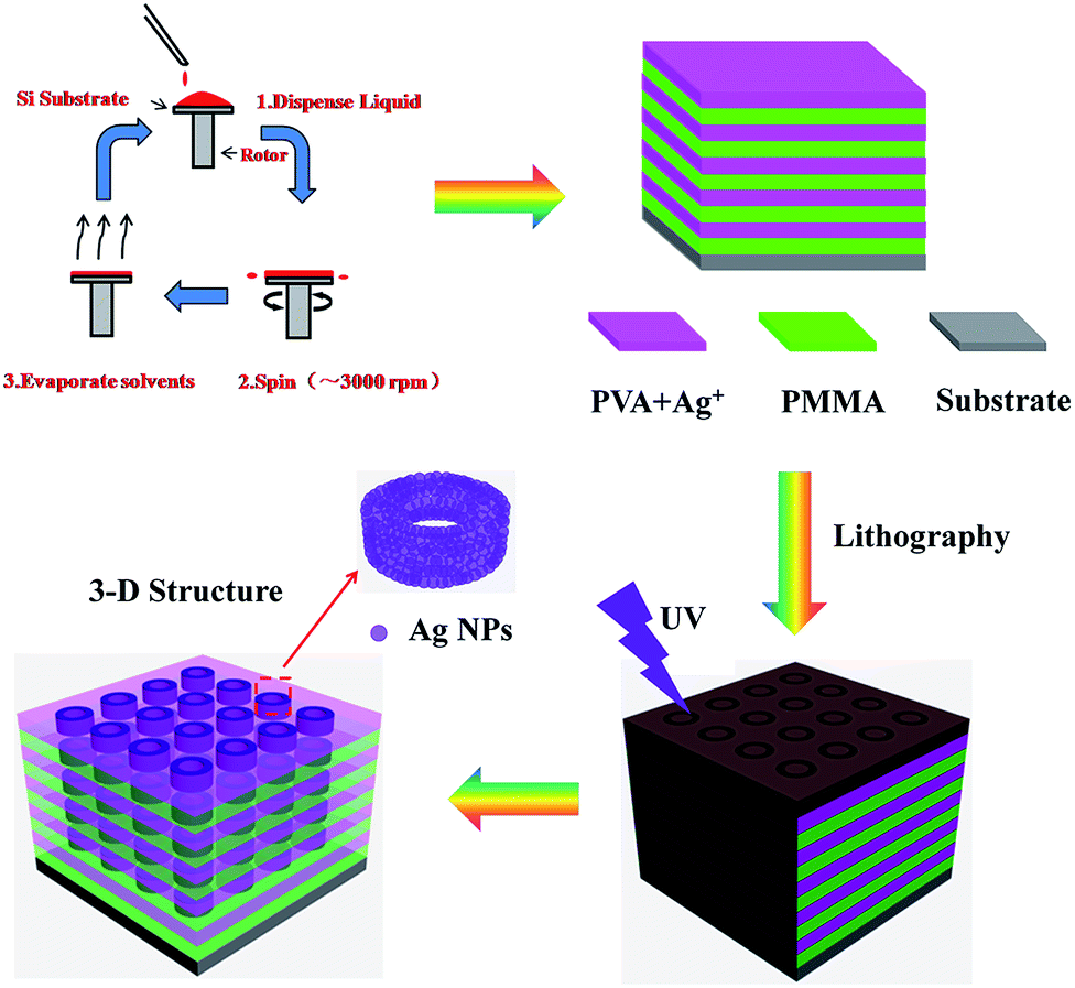 | ||
| Fig. 1 Schematic representation of the construction of a 3D structure derived from Ag ion doped 1D heterogeneous laminar stacks. | ||
Various building blocks can be produced by utilizing different photo-masks. Layered stacks may support smaller periods and the distance between building blocks can be adjusted by changing the internal film thickness, which we will discuss in detail in the following parts. Also, we make the silver-containing sol ahead of film fabrication, which affords accurate control of the amount of metal ions in the film over a large area. However, there are also limits in the utilization of such a method. One is that, because of the laminar character, and unlike direct laser writing producing 3D building blocks directly, this method is most applicable to fabricate stacked 3D structures. The other is that the size of building blocks is limited by the mask and irradiation source. Apart from the disadvantages above, fabricating 1D layers ahead of producing building blocks still provides us with an alternative way to construct stacked 3D structures.
Zero-valent silver NPs are formed during UV exposure
To verify the formation of silver NPs during the UV exposure, samples exposed to UV light directly without masks are tested. The reflectance spectrum of a 3-bilayer sample in its initial state is shown in Fig. 2a (black line). While after 30 min UV irradiation, an intense peak (around 76% reflectance for 1D layered stacks consisting of 3 bilayers) is observed at 630 nm (Fig. 2b, black line), and the reflectance ranging from 400 to 500 nm decreases dramatically compared to the initial state. We suspect that as a high-refractive index value component, silver NPs embedded in the PVA film bring optical change to the 1D layered system. The refractive indices for the PMMA and Ag+ containing PVA polymer layers are 1.474 and 1.481, respectively. The small difference between these two layers makes it difficult to achieve a photonic band within 3 bilayers.47,48 However, the silver NPs increased the refractive index of the PVA polymer films and the contrast between these two polymer films dramatically, thus satisfying all the conditions for being a typical one dimensional photonic crystal (1DPC) with an obvious photonic band. Strong absorption centered at 430–450 nm has been reported for silver containing PVA films,37 which may result in the reflection intensity decrease in the wavelength range of 400 to 500 nm. FDTD simulation was conducted here to confirm the experimental reflectance spectra (Fig. 2a and b, red lines). The parameters (refractive index, film thickness, number of layers, component material and incident angle) we used are based on our test results. Our experimental spectra (peak position and intensity) matched the simulation results very well except for the wavelength range of 400 to 540 nm in Fig. 2b which is attributed to the difference between the simulation model and practical situation. In practice, the increase of the RI value of the PVA film is induced by the embedded silver NPs. However, in the FDTD simulation, we establish a model of high and low RI value distribution instead of a metal–polymer composite film, thus surface plasmon resonance (SPR) absorption is not taken into consideration. That is the reason why the reflectance intensity is stronger in the simulated spectrum (Fig. 2b, red line). The sample after UV exposure exhibits a uniform and bright color (Fig. 2b) compared to that without UV curing (Fig. 2a) which is ascribed to the strong reflectance around 630 nm. The polymer–silver NPs composite film was studied by an ex situ measurement of the absorption spectrum. The single film exhibits an intense absorption centered at 450 nm (Fig. 2c) after UV exposure for 10 min under a mercury lamp (500 W, λ = 365 nm), which results from the Ag0 particles’ SPR absorbance.37 The morphology of the Ag NPs was characterized by TEM images. TEM samples were acquired from the same single film by immersing the quartz based PVA film into a HF/H2O (volumetric ratio = 1![[thin space (1/6-em)]](https://www.rsc.org/images/entities/char_2009.gif) :9, caution: Highly corrosive!) mixture for 10 s, and then lifting up a small piece of the single film with a carbon support film. Monodisperse silver NPs with an average diameter of 10 nm were observed (original TEM image is shown in Fig. S2†). In comparison to the particles in aqueous solution, the movements and aggregation of NPs were confined in the solid film. This contributes to the monodispersity of the silver NPs. The X-ray photoelectron spectroscopy (XPS) Ag 3d spectra of the Ag-containing PVA composite films were analyzed which further confirmed the reduction to form Ag0. As shown in Fig. 2d, the binding energy of the Ag 3d was observed at 368.25 eV and 374.25 eV with a spin energy separation of 6.0 eV, which would correspond to Ag0, indicating that the silver ions are mostly reduced to metallic silver NPs during the UV exposure.49 The cross sectional structure of the 1D laminar stacks before and after UV curing is shown in Fig. 2e and f. There were sharp interfaces between the layers representing a typical morphology of a 5 double-layer stack. The film thicknesses of the PVA and PMMA layers were 142 nm and 53 nm, respectively, which are in accordance with the results measured by a surface profiler and auto-laser ellipsometer. The choice of solvents is crucial for the successful building of the 1D multilayer structure, as we mentioned in the experimental part, we should always avoid mutual dissolution and penetration between different layers. Ag NPs embedded in PVA films are clearly shown in Fig. 2f. The size of the particles embedded in the bottom layers is relatively larger than of those in the upper layers; this can be explained by the nucleation and crystal growth theory.50,51 The growth typically follows an initial stage of nucleation; the amount of nuclei formed in the upper layers is larger than that in the bottom layers, because the UV light needs to penetrate the upper stacks to reach the bottom ones, which results in the size increase from the surface to the inner layers.
:9, caution: Highly corrosive!) mixture for 10 s, and then lifting up a small piece of the single film with a carbon support film. Monodisperse silver NPs with an average diameter of 10 nm were observed (original TEM image is shown in Fig. S2†). In comparison to the particles in aqueous solution, the movements and aggregation of NPs were confined in the solid film. This contributes to the monodispersity of the silver NPs. The X-ray photoelectron spectroscopy (XPS) Ag 3d spectra of the Ag-containing PVA composite films were analyzed which further confirmed the reduction to form Ag0. As shown in Fig. 2d, the binding energy of the Ag 3d was observed at 368.25 eV and 374.25 eV with a spin energy separation of 6.0 eV, which would correspond to Ag0, indicating that the silver ions are mostly reduced to metallic silver NPs during the UV exposure.49 The cross sectional structure of the 1D laminar stacks before and after UV curing is shown in Fig. 2e and f. There were sharp interfaces between the layers representing a typical morphology of a 5 double-layer stack. The film thicknesses of the PVA and PMMA layers were 142 nm and 53 nm, respectively, which are in accordance with the results measured by a surface profiler and auto-laser ellipsometer. The choice of solvents is crucial for the successful building of the 1D multilayer structure, as we mentioned in the experimental part, we should always avoid mutual dissolution and penetration between different layers. Ag NPs embedded in PVA films are clearly shown in Fig. 2f. The size of the particles embedded in the bottom layers is relatively larger than of those in the upper layers; this can be explained by the nucleation and crystal growth theory.50,51 The growth typically follows an initial stage of nucleation; the amount of nuclei formed in the upper layers is larger than that in the bottom layers, because the UV light needs to penetrate the upper stacks to reach the bottom ones, which results in the size increase from the surface to the inner layers.
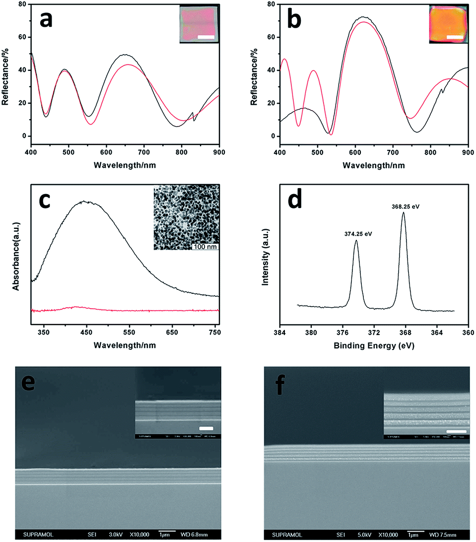 | ||
| Fig. 2 Reflectance spectra of a 3-bilayer sample before (a) and after (b) UV irradiation (black lines). Red lines are the corresponding results calculated by FDTD simulation. Insets are the photographs of the samples in the corresponding state, the scale bar is 1 cm. (c) Ex situ absorbance spectrum of Ag NPs composite films, the red line represents the sample before UV exposure while the black line is the same sample after UV exposure, inset is the TEM image of the silver NPs formed inside the films. (d) Ag 3d XPS spectrum of the silver NPs embedded PVA films. Cross sectional SEM images of the 1D layer stacks before (e) and after (f) UV curing, insets are corresponding magnified images, the scale bar for the inset images is 500 nm. | ||
Silver networks are obtained after UV curing under a photo-mask
The photo-reactive silver ions inside the 1D layered heterogeneous structure open a new way to build a 3D network structure. Making use of the chemical reaction of Ag+ under the external UV light instead of sophisticated physical management,52 a 3D structure was obtained. By selectively reducing the Ag+ in specific parts, different frameworks were formed according to the pre-designed photo-mask. As can be seen from Fig. 3a, a striped pattern with the size of 10 micrometers (μm) was observed under a microscope. During the exposure, the sample protected by the mask remained in the initial state, while the part without protection converted to zero valence Ag which changed the optical properties, thus giving the color contrast. With the same method, we also produced dots, concentric annuli, triangles and English letters on our samples. The size, shape and interval distance can all be modulated by previous design of the photo-masks. The smallest part of the letter K in the word ‘key’ (Fig. 3e) is 8 μm while the thinnest part of the letter D in ‘DNA’ (Fig. 3f) is 2 μm, which indicates that we can precisely modulate the pattern size on a minimum scale of around 5 μm. Besides micro pattern fabrication, we can also write macro letters by UV light in this multilayer matrix (Fig. S1†). ‘JLU’ was written on a 2 × 2 cm silicon substrate and the reflectance spectra of the letters and blank spaces were measured. The part exposed to UV light formed the ‘JLU’ pattern through Ag0 generation which produce a photonic stop band centered at 600 nm. A cross sectional SEM measurement was conducted along the border of an adjacent letter and blank space. As can be seen in Fig. S3,† there is an obvious difference in the amount of silver NPs along the fracture surface, which we define as the NPs barren and NPs rich parts. The NPs rich part belongs to the letter J while the NPs barren part belongs to the neighbouring space, which is protected by the photo-mask. Previous studies by Mills and co-workers reported that silver ions can be reduced by PVA in the dark,37 which explains why, even with the shield of the photo-mask, the silver ions are partly reduced in the NPs barren region. However, the UV light accelerates the reduction process, thus forming the NPs rich part. The difference in reaction rates also clearly verifies the effectiveness of modulating UV light to produce silver networks in selective parts of the 1D matrix. However, the silver ions remaining in the part with protection of the photo-mask may be reduced slowly when exposed to daylight. Even though this is a slow process when compared to the reduction under UV exposure, it may lead to the degradation of the as-prepared silver networks, which is a problem remained to be solved. A possible solution is adding a rinsing step after UV exposure to release the silver ions embedded in the polymer films. Considering that the PVA film is hydrophilic, water may infiltrate and then dissolve the ions, which is similar to a process described in a previous study.53 However, this needs more experiments to further verify and avoid further damage to the PVA films. The distance of zero-valence Ag belonging to different PVA layers can also be modulated by changing the thickness of the PMMA layers, which we will discuss in the following parts.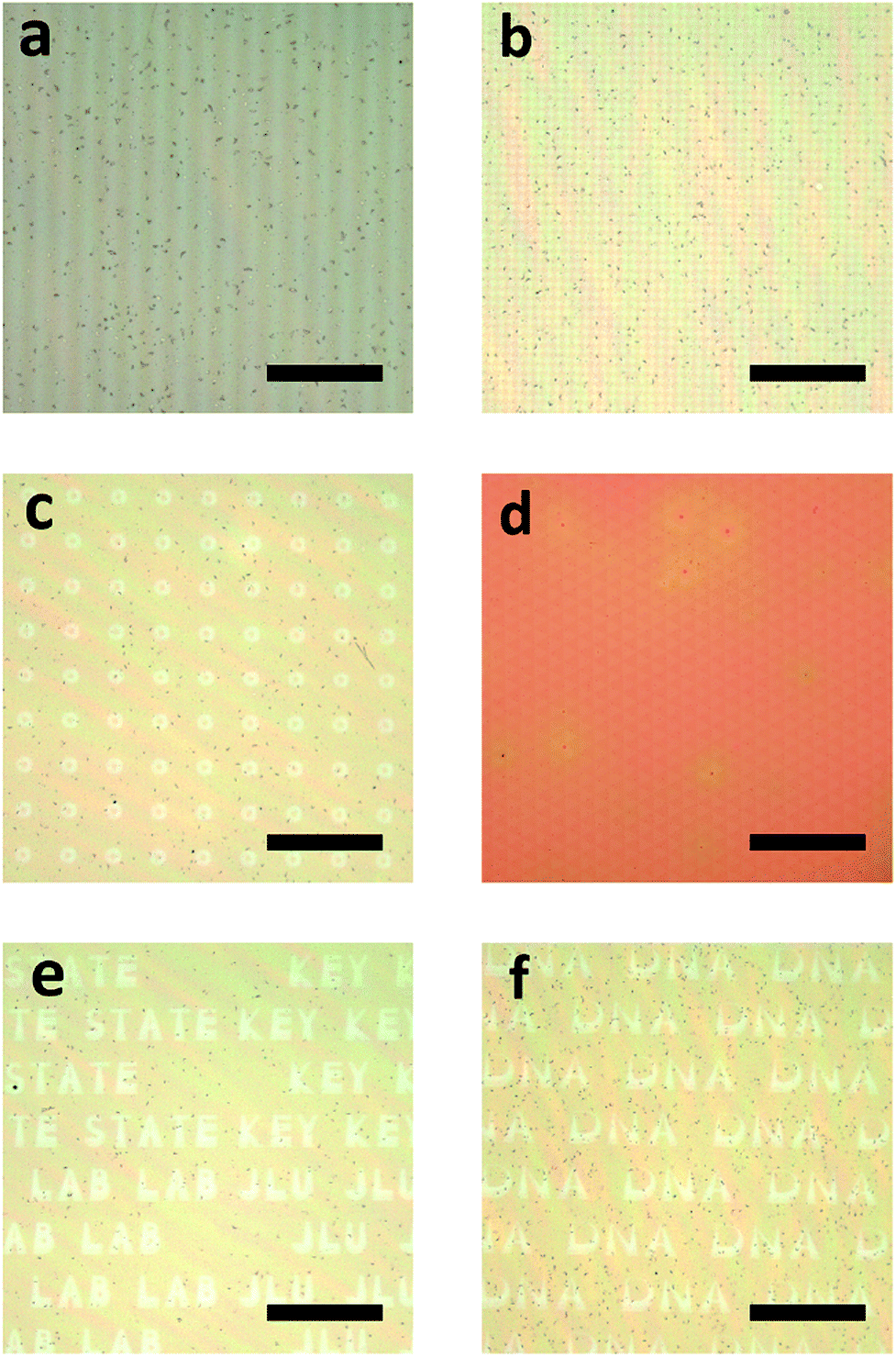 | ||
| Fig. 3 (a) Micrographs of the samples with (a) stripes, (b) dots, (c) concentric annuli, (d) triangles and (e and f) English letters from the top view, scale bars are all 200 μm except for (a) which is 100 μm. | ||
Fig. 2f verifies that the UV light can penetrate the whole stack and reach the bottom layer to conduct silver ion reduction, which indicates that the patterns we get above are not confined to the surface. Here, we take the sample, with a stripe pattern for example, to study the morphology inside the structure. For preparing the SEM sample, a photo-mask with 30 μm transparent and 50 μm opaque regions was utilized, and to match the scale of the mask, we specially fabricated a 1D structure with thicker layers (PVA 415 nm, PMMA 125 nm). Fig. 4a shows an illustrational process of the formation of silver building blocks. Zero valent silver NPs form after exposure to UV light and then aggregate according to the mask’s shape. The corresponding cross sectional SEM image of the as-prepared sample is shown in Fig. 4b. A periodical smooth and wrinkled morphology appears along the fracture surface and the difference between these two parts is so obvious that it could be easily identified. This can be ascribed to the mechanical property changes brought on by the Ag NPs. Because of the ductility of the polymer, the edges of the polymer tended to stretch after fracture, while for the body containing silver NPs, the rigidity increased, which contributed to the sharp interfaces. The lengths of the smooth and wrinkle parts are 30 μm and 50 μm, respectively, which correspond to the photo-mask. For smaller stripes with 10 μm alternate distribution, the cross sectional SEM images are shown in Fig. S4.† The same morphology of a periodical wrinkled and smooth distribution was also found, which correspond to the size scale of the mask. The part without protection of the photo-mask exhibited a smooth morphology after breakage, while the adjacent polymer layers were stretched and then curled. Our method produced metallic silver belonging to different layers from top to bottom in one step, which is easy to be put into mass production. The rectilinear propagation of UV light ensures the aligning of the building blocks in different layers instead of making alignment marks. Selecting a proper irradiation source according to the principle of light diffraction is also crucial for getting matched scale 3D networks.
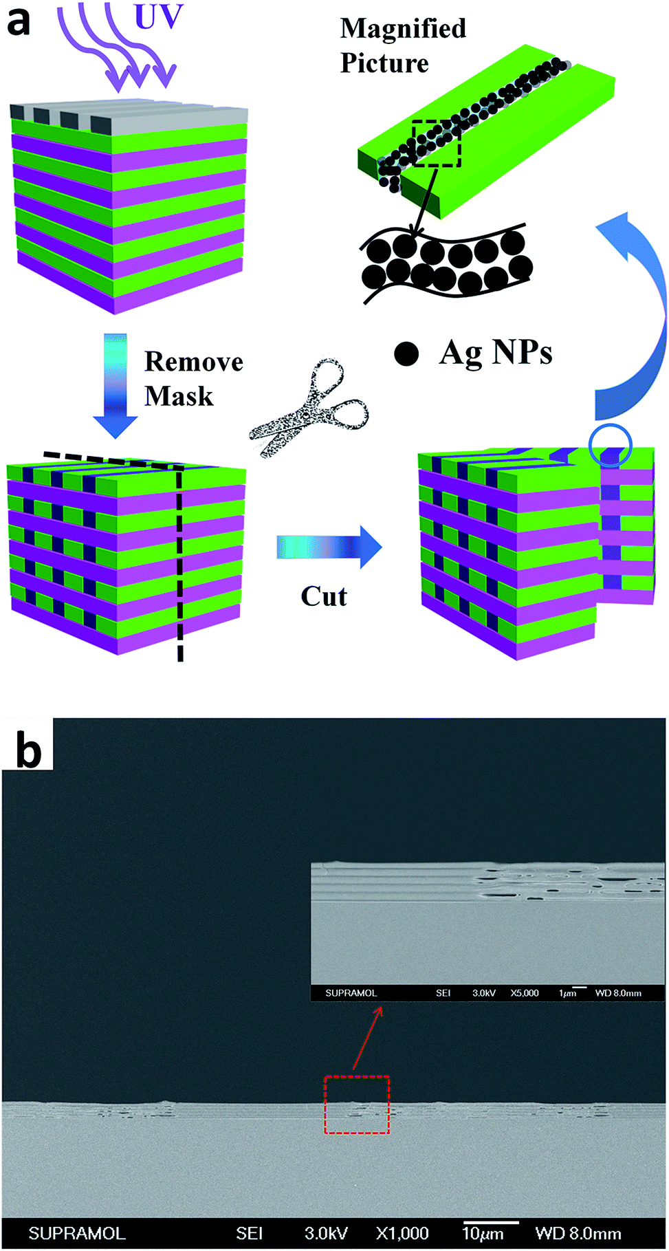 | ||
| Fig. 4 (a) Schematic illustration of the inner structure derived from a sample exposed to UV light with a striped mask, (b) cross sectional SEM image of a illustrational sample with a striped pattern. A periodical smooth and wrinkled morphology appears which corresponds to the photo-mask we used. | ||
Tracing the silver photo-generation process
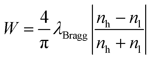
To understand how the UV curing time affects the silver reduction process, we analyze the reflectance spectra and the film RI value as a function of the UV exposure time. Starting from the Ag+ doped 1D ordered layers, the reflectance intensity increased dramatically after 70 min UV exposure from 55% to 85%, as shown in Fig. 5a, and the position of Bragg peak was finally located at 670 nm. When compared to the initial state, the position of the stop band blue-shifted, which resulted from the broadening of the half-peak width.54 The band width can be calculated by the following equation:where W is the band width, λBragg is the peak position, and nh and nl are the refractive indices of the high-index and low-index layers, respectively. As mentioned above, silver NPs increased the refractive index (nh) of the PVA layer, thus increasing the value of (nh − nl)/(nh + nl), resulting in the broadening of the band width. Fig. 5b shows the time-dependent change of the reflectance intensity marked by ΔR/R, where the value of ΔR was defined as the real time reflectance minus the initial reflectance (R). The refractive index of the silver composite single film under UV irradiation for various times is shown in the inset of Fig. 5b. At the beginning, the reflectance intensity increased linearly, and after 45 min UV exposure it reached a plateau, which is in perfect agreement with the rising trend of the single film’s RI. The silver composite single film absorption was measured (Fig. S5†), and the intensity of absorption increased with the exposure time. At the beginning, it increased very fast until 20 minutes was reached, which is in good accordance with the change of RI value. The increase of the film absorption verified the rising amount of silver NPs, and more NPs gave a higher refractive index of the composite film, which resulted in an obvious photonic band. This explains very well that the changing trends of reflection intensity, RI value and absorption intensity match one another. In order to study whether there is difference between the percentage of silver as reduced metal in the top and bottom PVA layers, a group of multilayer samples on a quartz glass substrate were prepared. The results are shown in Fig. S6,† from which we can see that after a certain period of UV exposure, most of the silver ions in the multilayer structure, including those embedded in the bottom PVA layers, are reduced to zero-valent silver metal.
 | ||
| Fig. 5 (a) Time-dependent reflectance spectra of the silver doped laminar stacks. (b) Time-dependent change of reflectance intensity, inset is the increase of the refractive index of a single composite film during UV curing. | ||
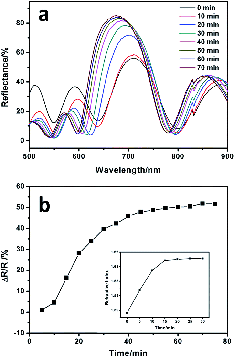
Next, the reflectance spectra and film RI value are measured as a function of silver nitrate doping amount. Fig. 6a to e show the reflectance spectra of samples with different amounts of AgNO3, ranging from 0.01 to 0.05, in the PVA/AgNO3 precursor solution (g ml−1), and Fig. 6f summarizes the changing trend. The larger Ag amount gave a higher reflection value before it reached 0.03 g ml−1. This can be attributed to more silver ions in the precursor solution, resulting in a larger silver particle fraction in the composite film, which leads to a higher RI value after photo-reduction. On the contrary, further increasing the quantity of AgNO3 generated a decline of the reflection. This phenomenon can be explained by the phase separation brought on by the addition of inorganic silver NPs. Microphotographs of the corresponding samples with Ag content, in weight percent, of 14.2% (Fig. 6h), 33.1% (Fig. 6i) and 41.2% (Fig. 6j) in the composite films, measured by EDS, showed the phase behaviours. A uniform and smooth film was generated from reactive silver-containing precursors followed by in situ photo-reduction at lower Ag fraction, while a higher Ag fraction (above 33.1 wt%) generated stripes, which is caused by the phase separation in the organic–inorganic composite films. This may increase the light scattering inside the multilayer system and subsequently enhance the energy loss, which leads to the decrease of the total reflection. Thus, in the following study, we only prepare the composite multilayer structure with a silver content no higher than 33.1 wt% for various tests in order to limit the energy loss to a reasonable level. The refractive indices of the composite films were measured at 632.8 nm by an ellipsometer (Fig. 6g). Starting from 1.4836, the RI value of the Ag-containing film reached 1.7892 at 43.35 wt%. We can also see that the RI value has no linear dependence on the Ag weight content, which is in good agreement with previous work on PbS/polymer film.55 Based on the aforementioned discussion, it is clear that as a high-RI value content, Ag NPs have a great contribution to the increase of the composite films’ refractive indices, which produced a large contrast between the PVA/Ag layer and the PMMA layer. A higher Ag weight fraction brought higher RI values, while larger content of inorganic Ag NPs embedded in the polymer film also produced phase separation. Taking both RI and phase performance into consideration, 0.03 g AgNO3 in 1 milliliter precursor solution meets both sides and it brought about the strongest reflection among various silver doping amounts when other parameters (layer thickness, number of layers and incident angel) were the same.
 | ||
| Fig. 6 (a) to (e) are the reflectance spectra of the multilayer structure containing different amounts of AgNO3, ranging from 0.01 g to 0.05 g, dissolved in 1 ml PVA aqueous solution. Black lines represent the original state before UV irradiation while red lines are the reflectance spectra after 40 min UV exposure. (f) Summary of the change of the reflectance intensity defined by ΔR/R as a function of the AgNO3 doping amount (g/10 ml). (g) The RI values of the silver NPs composite film after UV curing as a function of silver doping amount (atomic weight percentage measured by EDS). (h)–(j) are the microphotographs of the composite film containing 0.01, 0.03 and 0.05 g silver nitrate in 1 milliliter precursor solution, respectively (scale bars are all 50 μm). | ||
Manipulation of the matrix structure
Building a one dimensional layered matrix ahead of 3D construction not only brings convenience for generating building blocks at one time, but also provides a free tuning matrix for structural diversity. As we mentioned above, the building of multilayers qualifies the material as a real 3D structure, thus the total number of layers is one of the key parameters which affects the structural properties. Our 1D matrix can act as a model with a convertible number of layers. Increasing the number of layers will add repeating building blocks and thus enhance the mutual interaction inside our 3D structure, which is a good model to study. In our 1D layered system, because of the contribution of the Ag NPs to reinforce the RI contrast between the PMMA and PVA layers, increasing layer number will add saturation to replicate colors more vividly, because it enhances the reflection intensity.56Fig. 7 shows the reflectance spectra of the 1D laminar structure with various number of bilayers. For the sample with only 3 bilayers, the reflectance intensity reached 73%, and when the number of bilayers increased to 6, an intense peak (above 90%) was observed at 635 nm, which had a negligible red shift of the Bragg peak position, and the band width became narrower. The structural measurement by SEM is shown in Fig. S7;† the sharp interfaces between different layers make it easy for us to distinguish the samples with layer numbers from 3 to 6, and the photographs also show that the color saturation of the 6-bilayer sample is the highest among the four samples, which is brought on by the narrower bandwidth and stronger reflection. We also successfully built layered structures with 11 and 14 bilayers; their cross section is shown in Fig. S8.† There is no dissolution and penetration which indicates that our 1D matrix has good flexibility in changing the total number of layers.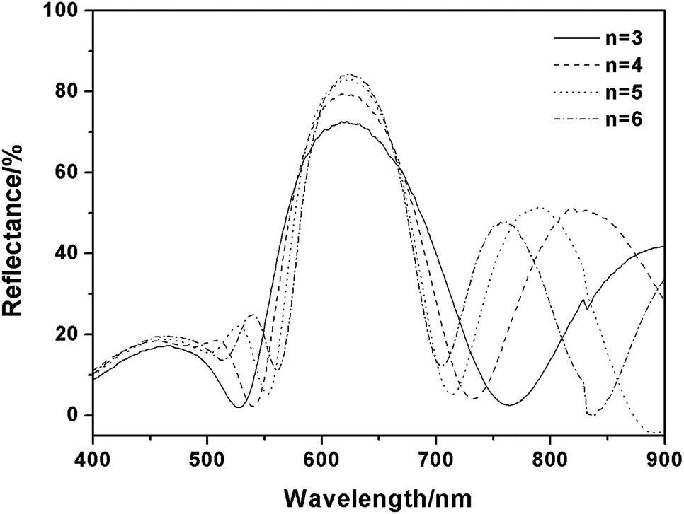 | ||
| Fig. 7 Adjusting the reflectance intensity of the 1D multilayer structure based on 1DPC theory by varying the number of bilayers (n). | ||
Besides the total number of layers, the layer thickness is also crucial to manipulate the layer structure. Usually it can be realized by either varying the polymer solution concentration (i.e. the solution viscosity) or the rotation speed/spin time. Here, we first fixed the precursor solution concentration and spin time, and lowered the rotation speed for each layer to 3000 rpm, 2500 rpm and 2000 rpm to fabricate three samples. The change of the film thickness is reflected in the SEM images and the shift of the peak position. Cross sectional SEM images are shown in Fig. 8a–c. The thicker part consists of PVA, while the thinner part is a PMMA layer. The thicknesses of the PVA layers in Fig. 8a–c are 92 nm, 97 nm and 106 nm, and the thicknesses of the PMMA layers are 30 nm, 38 nm and 44 nm, respectively. The increase of the period thickness resulted in the red shift of the Bragg peak position. As shown in Fig. 8d, the peak position was centered at 556 nm, 605 nm and 652 nm, respectively, which shifted towards a longer wavelength. The photographs in Fig. 8d present vivid color, which correspond to the three samples we mentioned above. However, in some cases of stacked 3D structures containing repeating building blocks which have strong interactions between interval layers,57 precisely controlling the distance between these layers is highly demanded, i.e. the thickness of PMMA layers.58 To realize this purpose, we spin coated a fixed concentration PVA solution together with various concentrations of PMMA solution, and the results are shown in Fig. S9.† SEM images show the cross section fracture which exhibits a clear alternate layer distribution, the PVA layers in all three samples possess the same layer thickness of 102 nm, while the thickness of the PMMA layers increases from 40, 46 to 53 nm. Using this method, we can freely adjust the thickness of spacer layers to provide a flexible matrix for studying the interaction between building blocks. However, in practical application, we do not need to take SEM measurements to trace the variation of period thickness, it can be verified by the peak red shift in reflectance spectra (Fig. S9d†). The adjustment of PVA layer thickness through tuning PVA solution concentration was shown in Fig. S10,† with a fixed PMMA layer thickness of 38 nm and a PVA layer thickness varying from 90, 118 to 140 nm. By using the methods we mentioned above, our 1D layered structure proves to be a perfect matrix for 3D construction.
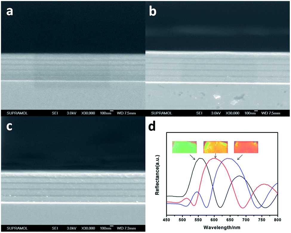 | ||
| Fig. 8 Cross sectional SEM images of the 1DPCs consisting of different layer thicknesses: (a) PVA layer is 92 nm and PMMA layer is 30 nm; (b) PVA layer is 97 nm and PMMA layer is 38 nm; (c) PVA layer is 106 nm and PMMA layer is 44 nm. (d) is the corresponding reflectance spectra of the sample (a)–(c) from left to right; insets in (d) are photographs of the three samples (2 × 1 cm). | ||
Experimental
Materials
Poly(vinyl alcohol) (PVA) (Mw 13000–23000) and poly(methyl methacrylate) (PMMA) with a Mw of 120000 were purchased from Aldrich. Silver nitrate was obtained from Aladdin. All the reagents were used as received without further purification. Silicon wafers (100) were cut into 2 × 2 cm small pieces followed by cleaning in boiling piranha solution (a mixture of 98% H2SO4/30% H2O2 with volumetric ratio 7:3, caution: this solution is extremely corrosive!) and then rinsing in DI water 3 times before use.
Fabrication of Ag+ precursor doped 1D heterogeneous layer structure
The multifilms were fabricated on the as-prepared silicon wafers. In detail, PMMA and PVA were first dissolved in toluene and DI water, respectively, via ultrasonic treatment, then the desired amount of AgNO3 was added into the aqueous solution of PVA to form Ag+ doped precursor solution. The 1D layers were fabricated by spin coating the PVA and PMMA sol alternately at 3000 rpm for 60 s, and each layer was baked at 80 °C for 10 min. The first layer was PMMA and the last layer was PVA in all our samples. All the operations were conducted in the dark to avoid light reduction of the silver ions. The thickness of each layer can be adjusted by changing the concentration of the precursor solution or the rotation speed. The total number of layers was calculated as 2n.The selection of the solvents for each polymer layer played a very important role in the preparation of pure polymer layered stacks. We chose deionized water for dissolving PVA and silver nitrate together and toluene for dissolving PMMA. Toluene is an excellent solvent for PMMA and a poor solvent for PVA which can help form a perfect PMMA thin film without destroying the PVA film. Similarly, deionized water is an excellent solvent for PVA and a poor solvent for PMMA which can help form a perfect PVA thin layer without destroying the PMMA layer. The choice of solvents also involved penetrability. In our design, toluene cannot penetrate the PVA layer and deionized water cannot penetrate the PMMA layer, which ensured the acquisition of the multilayer 1D matrix.
In situ photo-reduction of Ag+ to form Ag NPs inside the layer structure
Silver NPs were formed by exposing the as-prepared laminar structure sample to UV irradiation (500 W, λ = 365 nm) for a preset time at room temperature. The UV curing system was equipped with an ACM mirror and cooling system for temperature reduction.Photo induced 3D frameworks inside 1D layer stacks
The 3D structured silver skeleton was produced by UV reduction of the sample with a pre-designed photo-mask. Based on the different patterns of the photo-mask, the silver skeleton formed inside every PVA layer will exhibit corresponding stripes, dots, triangles or English letters. During the exposure process, the mask is strictly fixed on top of the 1D layer stack to ensure the alignment of the silver NPs from the sample surface to the bottom, thus forming a perfect skeleton inside the 1DPC.Finite-difference time-domain (FDTD) calculations
The calculated reflectance spectra were obtained using the commercialized software package, FDTD Solutions (Lumerical Solutions, Inc., Canada). A two-dimensional simulation region was employed in the XY plane. A periodic boundary condition was set in the ±Y direction and two perfectly matched layers in the ±X direction. The incident plane waves were perpendicular to the sample surfaces. The layer thicknesses and refractive indices of the simulation models were set according to those of the corresponding fabricated samples.Characterization
A Shimadzu 3600 UV-VIS-NIR spectrophotometer was used to measure the absorbance and reflectance spectra. The cross sectional micrographs were taken with a JEOL FESEM 6700F scanning electron microscope (SEM), and all the samples were sputtered with a thin layer of Pt before testing. The size of the photoreduced silver nanoparticles was determined by a Hitachi H-800 transmission electron microscope (TEM). An Electronic Data Systems (EDS) analyzer attached to the JEOL FESEM 6700F scanning electron microscope operating in SEI mode was used to analyze the Ag formed in the composite films. An X-ray photoelectron (XPS) test using Mg-Kα excitation (1253.6 eV) of the silver-containing composite films was collected with a VG ESCALAB MKII spectrometer. Binding energy calibration was based on C 1s at 284.6 eV. The thickness of PVA and PMMA single layers was measured by a Dektak 150 surface profiler (Veeco). The refractive indices of the polymer thin films at a wavelength of 632.8 nm were measured on an AUEL-III auto-laser ellipsometer equipped with a He–Ne laser (λ = 632.8 nm). The microphotographs were taken with an Olympus BX 51. Digital camera photographs were shot with a Canon Powershot G1X.Conclusion
A 3D ordered structure has been constructed by conducting a photo-reduction process in a Ag ion doped heterogeneous 1D structure. Employing the reaction between UV light and Ag+ opens up a new way to fabricate 3D networks inside the multilayers. By selectively photo-reducing the part without protection, our method realizes the formation of Ag NPs belonging to different layers in one step. The alignment of the silver building blocks belonging to different layers is simply guaranteed by the rectilinear propagation of UV light instead of a complex and repeating aligning process. The embedded silver NPs also dramatically increase the refractive index value of the PVA layers, thus resulting in an obvious PBG with fewer layers, which provides us with a method to trace the silver formation process. The number of layers and the distance between adjacent silver lattice layers can be precisely tuned as needed. For chasing a more delicate structure, shorter wavelength light should be applied as the radiation source to produce building blocks with much smaller size by avoiding light diffraction. We believe that further study will help reveal the potential use of our structure in fields such as bioassays and SERS matrices, and especially photonic meta-materials with working frequencies in the optical range can be envisioned based on our chemical approach.Acknowledgements
This work was financially supported by the National Science Foundation of China (NSFC) under Grant no. 91123031, 21221063, 51373065 and the National Basic Research Program of China (973 Program) under Grant no. 2012CB933800.Notes and references
- D. G. Stavenga, S. Foletti, G. Palasantzas and K. Arikawa, Proc. R. Soc. London, Ser. B, 2006, 273, 661 CrossRef CAS PubMed.
- M. Srinivasarao, Chem. Rev., 1999, 99, 1935 CrossRef CAS PubMed.
- P. Vukusic and J. R. Sambles, Nature, 2003, 424, 852 CrossRef CAS PubMed.
- A. R. Parker and H. E. Townley, Nat. Nanotechnol., 2007, 2, 347 CrossRef CAS PubMed.
- Q. F. Cheng, M. Z. Li, L. Jiang and Z. Y. Tang, Adv. Mater., 2012, 24, 1838 CrossRef CAS PubMed.
- J. G. Fleming and S. Y. Lin, Opt. Lett., 1999, 24, 49 CrossRef CAS PubMed.
- O. Jeon and E. Alsberg, Adv. Funct. Mater., 2013, 23, 4765 CAS.
- J. Valentine, S. Zhang, T. Zentgraf, E. Ulin-Avila, D. A. Genov, G. Bartal and X. Zhang, Nature, 2008, 455, 376 CrossRef CAS PubMed.
- N. Liu, H. C. Guo, L. W. Fu, S. Kaiser, H. Schweizer and H. Giessen, Nat. Mater., 2008, 7, 31 CrossRef CAS PubMed.
- J. X. Wang, Y. Z. Zhang, S. T. Wang, Y. L. Song and L. Jiang, Acc. Chem. Res., 2011, 44, 405 CrossRef CAS PubMed.
- A. Biswas, I. S. Bayer, A. S. Biris, T. Wang, E. Dervishi and F. Faupel, Adv. Colloid Interface Sci., 2012, 170, 2 CrossRef CAS PubMed.
- J. E. E. Baglin, Appl. Surf. Sci., 2012, 258, 4103 CrossRef CAS.
- Y. L. Zhang, Q. D. Chen, H. Xia and H. B. Sun, Nano Today, 2010, 5, 435 CrossRef CAS.
- S. M. George, Chem. Rev., 2010, 110, 111 CrossRef CAS PubMed.
- R. W. J. Scott, S. M. Yang, N. Coombs, G. A. Ozin and D. E. Williams, Adv. Funct. Mater., 2003, 13, 225 CrossRef CAS.
- B. Su, S. T. Wang, Y. C. Wu, X. Chen, Y. L. Song and L. Jiang, Adv. Mater., 2012, 24, 2780 CrossRef CAS PubMed.
- G. R. Xiong, G. Z. Han, C. Sun, H. Xu, H. M. Wei and Z. Z. Gu, Adv. Funct. Mater., 2009, 19, 1082 CrossRef CAS.
- J. Liu, Y. Mao and J. Ge, Nanoscale, 2012, 4, 1598 RSC.
- Y. Aizawa, R. Wylie and M. Shoichet, Adv. Mater., 2010, 22, 4831 CrossRef CAS PubMed.
- M. E. Kolewe, H. Park, C. Gray, X. F. Ye, R. Langer and L. E. Freed, Adv. Mater., 2013, 25, 4459 CrossRef CAS PubMed.
- W. H. Peng, S. M. Zhu, W. L. Wang, W. Zhang, J. J. Gu, X. B. Hu, D. Zhang and Z. X. Chen, Adv. Funct. Mater., 2012, 22, 2072 CrossRef CAS.
- D. R. Smith, W. J. Padilla, D. C. Vier, S. C. Nemat-Nasser and S. Schultz, Phys. Rev. Lett., 2000, 84, 4184 CrossRef CAS PubMed.
- C. M. Soukoulis, S. Linden and M. Wegener, Science, 2007, 315, 47 CrossRef CAS PubMed.
- C. M. Soukoulis and M. Wegener, Science, 2010, 330, 1633 CrossRef CAS PubMed.
- C. R. Simovski, P. A. Belov, A. V. Atrashchenko and Y. S. Kivshar, Adv. Mater., 2012, 24, 4229 CrossRef CAS PubMed.
- H. O. Moser and C. Rockstuhl, Laser Photonics Rev., 2012, 6, 219 CrossRef CAS.
- F. Monticone and A. Alù, Chin. Phys. B, 2014, 23, 047809 CrossRef.
- Z. Li, M. Mutlu and E. Ozbay, J. Opt., 2013, 15, 023001 CrossRef.
- M. Kadic, T. Bückmann, R. Schittny and M. Wegener, Rep. Prog. Phys., 2013, 76, 126501 CrossRef PubMed.
- J.-H. Lee, J. P. Singer and E. L. Thomas, Adv. Mater., 2012, 24, 4782 CrossRef CAS PubMed.
- C. M. Soukoulis and M. Wegener, Nat. Photonics, 2011, 5, 523 CAS.
- D. R. Clary and G. Mills, J. Phys. Chem. C, 2011, 115, 14656 CAS.
- J. G. Zhang, S. Q. Xu and E. Kumacheva, Adv. Mater., 2005, 17, 2336 CrossRef CAS.
- K. K. Chia, R. E. Cohen and M. F. Rubner, Chem. Mater., 2008, 20, 6756 CrossRef CAS.
- G. Machado, M. M. Beppu, A. F. Feil, C. A. Figueroa, R. R. B. Correia and S. R. Teixeira, J. Phys. Chem. C, 2009, 113, 19005 CAS.
- A. S. Korchev, T. Konovalova, V. Cammarata, L. Kispert, L. Slaten and G. Mills, Langmuir, 2006, 22, 375 CrossRef CAS PubMed.
- G. A. Gaddy, A. S. Korchev, J. L. McLain, B. L. Slaten, E. S. Steigerwalt and G. Mills, J. Phys. Chem. B, 2004, 108, 14850 CrossRef CAS.
- B. V. Lotsch, C. B. Knobbe and G. A. Ozin, Small, 2009, 5, 1498 CrossRef CAS PubMed.
- T. A. Baker, O. L. A. Monti and D. J. Nesbitt, J. Phys. Chem. C, 2011, 115, 9861 CAS.
- A. S. Korchev, M. J. Bozack, B. L. Slaten and G. Mills, J. Am. Chem. Soc., 2004, 126, 10 CrossRef CAS PubMed.
- N. Marquestaut, Y. Petit, A. Royon, P. Mounaix, T. Cardinal and L. Canioni, Adv. Funct. Mater., 2014, 24, 5824 CrossRef CAS.
- K. Shimizu and A. Satsuma, Phys. Chem. Chem. Phys., 2006, 8, 2677 RSC.
- T. V. Slenters, I. Hauser-Gerspach, A. U. Daniels and K. M. Fromm, J. Mater. Chem., 2008, 18, 5359 RSC.
- N. Leopold and B. Lendl, J. Phys. Chem. B, 2003, 107, 5723 CrossRef CAS.
- A. Klinkova, R. M. Choueiri and E. Kumacheva, Chem. Soc. Rev., 2014, 43, 3976 RSC.
- N. Liu, H. Guo, L. Fu, S. Kaiser, H. Schweizer and H. Giessen, Nat. Mater., 2007, 7, 31 CrossRef PubMed.
- Z. Wang, J. Zhang, J. Xie, Z. Wang, Y. Yin, J. Li, Y. Li, S. Liang, L. Zhang, L. Cui, H. Zhang and B. Yang, J. Mater. Chem., 2012, 22, 7887 RSC.
- D. Owens, C. Fuentes-Hernandez and B. Kippelen, Thin Solid Films, 2009, 517, 2736 CrossRef CAS.
- H. Kong and J. Jang, Chem. Commun., 2006, 3010 RSC.
- J. Zeng, C. Zhu, J. Tao, M. S. Jin, H. Zhang, Z.Y. Li, Y. M. Zhu and Y. N. Xia, Angew. Chem., Int. Ed., 2012, 51, 2354 CrossRef CAS PubMed.
- K. Yu, X. Y. Liu, Q. Zeng, M. L. Yang, J. Y. Ouyang, X. Q. Wang and Y. Tao, Angew. Chem., Int. Ed., 2013, 52, 11034 CrossRef CAS PubMed.
- Y. Zhou, S. H. Yu, C. Y. Wang, X. G. Li, Y. R. Zhu and Z. Y. Chen, Adv. Mater., 1999, 11, 850 CrossRef CAS.
- C. Damm and H. Münstedt, Appl. Phys. A, 2008, 91, 479 CrossRef CAS.
- E. Redel, J. Mlynarski, J. Moir, A. Jelle, C. Huai, S. Petrov, M. G. Helander, F. C. Peiris, G. von Freymann and G. A. Ozin, Adv. Mater., 2012, 24, OP265 CrossRef CAS PubMed.
- C. L. Lu, C. Guan, Y. F. Liu, Y. R. Cheng and B. Yang, Chem. Mater., 2005, 17, 2448 CrossRef.
- V. A. Tolmachev, A. V. Baldycheva, E. Y. Krutkova, T. S. Perova and K. Berwick, Modeling Aspects in Optical Metrology II, 2009, vol. 7390, p. 739017 Search PubMed.
- A. E. Miroshnichenko, B. Luk’yanchuk, S. A. Maier and Y. S. Kivshar, ACS Nano, 2012, 6, 837 CrossRef CAS PubMed.
- C. Garcia-Meca, J. Hurtado, J. Marti, A. Martinez, W. Dickson and A. V. Zayats, Phys. Rev. Lett., 2011, 106, 067402 CrossRef PubMed.
Footnote |
| † Electronic supplementary information (ESI) available: Detailed characterization of the patterned sample, SEM measurement of the 3D structure, absorbance spectrum of a single composite film and structural variation as function of layer numbers and layer thickness, respectively, are given. See DOI: 10.1039/c4ra17258b |
| This journal is © The Royal Society of Chemistry 2015 |