
Nonvolatile memory devices based on carbon nano-dot doped poly(vinyl alcohol) composites with low operation voltage and high ON/OFF ratio†
Lingqiang Mengabc,
Minhuan Lanabc,
Liang Guoabc,
Lisha Xied,
Hui Wangabc,
Jiechao Geab,
Weimin Liuab,
Ying Wang*ab and
Pengfei Wangab
aKey Laboratory of Photochemical Conversion and Optoelectronic Materials, Technical Institute of Physics and Chemistry, Chinese Academy of Sciences, Beijing, 100190, China. E-mail: wangy@mail.ipc.ac.cn
bKey Laboratory of Photochemical Conversion and Optoelectronic Materials and CityU-CAS Joint Laboratory of Functional Materials and Devices, Technical Institute of Physics and Chemistry, Chinese Academy of Sciences, Beijing, 100190, China
cUniversity of Chinese Academy of Sciences, Beijing, 100049, China
dCollege of Life Science and Technology, University of Chemical Technology, Beijing, China
First published on 6th March 2015
Abstract
Carbon nano-dots were synthesized by a hydrothermal method and integrated into the poly(vinyl alcohol) matrix as charge carrier trapping centers for nonvolatile memory devices. The devices with the configuration of ITO/carbon nano-dots-PVA/Ag exhibited bistable electrical switching at low voltage, long retention time and excellent reading stability.
Nonvolatile memory devices based on hybrid organic–inorganic nano-composites have been considered to be excellent candidates for promising application in next-generation electronics due to their advantages, such as low cost, simple device configuration, low temperature processing, large scale manufacturing, and good compatibility with flexible substrates.1–4 Considerable efforts have been undertaken both in academia and industry to obtain high performance organic memory devices,5–7 and lots of nanoparticles have been used as the charge trapping centres for the active layer, such as metal nanoparticles,7 metal oxide semiconductors,8–10 fullerenes,5 carbon nanotubes,11 graphene, graphene quantum dots (QDs) or graphene oxides.12–14 Chu et al. used the hybrid ZnO nano-rod/polymethylmethacrylate (PMMA) hetero-structures as the electrically bistable materials for the bistable random access memory devices.15 Kim et al. reported the nonvolatile memory devices based on multi-walled carbon nano-tubes/poly-4-vinyl-phenol (PVP) composites.11 H. Zhang et al. reported a flexible memory diode with the configuration of reduced graphene oxide/MoS2–PVP/Al.9 Although much progress have been achieved, there are still some obstacles impeding them from practical applications. One of them is the low ON/OFF ratio (<104) and high operation voltage of the bi-stable devices. The embedded nanoparticles are inclined to the aggregation, such as graphene QDs or graphene oxides.12–14 The aggregation of the nanoparticles and the thus short-circuit between the aggregations can increase the OFF current of the memory devices, leading to the low ON/OFF ratio. The large switching voltage can be ascribed to the high hetero-material interface energy barriers, resulting in the high voltage for the injection of charge carriers from electrodes. Also, the toxic solvents were also needed during the blending of organic matrix and nanoparticles, which is undesirable for the manufacture and application. Thus, high performance nonvolatile memory devices with low operating voltage and large ON/OFF ratio is still a challenge.
Carbon nano-dots are 0D quasi-spherical carbon nanoparticles with size below 10 nm.16 Their fascinating chemical, electronic and optical properties, such as excellent water solubility, stable photoluminescence, low cytotoxicity, excellent biocompatibility and cell membrane permeability, had paved the way towards photocatalyst, energy conversion/storage, quantitative detection, and highly efficient fluorescent imaging.17–20 Especially in the electronics, Wang et al. demonstrated the first white light-emitting device with the carbon dots as the active layer, getting a maximum external quantum efficiency of 0.083% at a current density of 5 mA cm−2 with a colour rendering index of 82.21 The carbon nano-dots can be regarded as the analogues of the aggregation of carbon nanotube or graphene, the graphene or carbon nanotube parts aggregating together with the functional group outward. P. Mirtchev et al. had used carbon quantum dots (QDs) as a sensitizer in a dye-sensitized solar cell, achieving a power conversion efficiency of 0.13%.22 Zhu et al. inserted an ultrathin layer graphene QDs between perovskite and TiO2 as the superfast electron tunnel to enhance the electron extraction, leading to a significant power conversion efficiency improvement of perovskite solar cells from 8.81% to 10.15%.23 However, there is no report on the application of carbon nano-dots for the organic memory devices. The success of graphene QDs as the electron-acceptor materials for polymer photovoltaic devices inspired us to innovatively use the carbon nano-dots as the charge trapping centres of the organic memory devices.17 In this communication, we reported the first organic nonvolatile memory device using carbon nano-dots as the carrier-trapping centres. The resulting devices exhibits low operating voltages of 1 V (turn-on) and −3 V (turn-off), and the ON- and OFF-states possess a retention time of over 3500 s with a high ON/OFF ratio up to 105, which is promising for memory cells with low power consumptions.
The hydrothermal preparation of carbon nano-dots was performed (see the Experimental section in the ESI†). The carbon nanodots solution of water remains homogeneous even at room temperature without any perceptible changes. The UV-vis absorption spectrum of the as-prepared carbon nano-dots in water displays a broad absorption band up to 600 nm (Fig. 1). With increasing excitation wavelength from 340 to 500 nm, the PL emission peak with the reduced PL intensity redshifts from 461 to 566 nm. Similar excitation-dependent feature can also be observed for the PL emission spectra of the as-prepared carbon nano-dots as previously reported. The multicolour emission reflect the effects from particles of different sizes and the distribution of different surface states on the surface of carbon nano-dots.24 TEM images reveal that the carbon nano-dots are mono-dispersed and have a uniform diameter of 2–8 nm (Fig. 1c–e), corresponding to d-spacing values of 2.8 Å. The d-spacing values are close to the value for the planes of (020) graphitic carbon, indicating the graphitic nature of the carbon nano-dots.25 These are comparable to those carbon QDs synthesized by electrochemical methods or thermal pyrolysis.17,26 The corresponding AFM images show that there typical topographic heights were between 0.7–3.5 nm, similar to the synthesized graphene QDs consisting of 2–10graphene layers.17
 | ||
| Fig. 1 (a and b) UV-vis absorption and photoluminescence spectra of carbon nano-dots in water, respectively; (c and d) TEM and HRTEM images of as-prepared carbon nano-dots; (e) sized distribution of carbon nano-dots; (f) AFM image of the carbon nano-dots on Si substrate (the height profile along the line); (g) FT-IR spectra of carbon nano-dots; (h) the C1s XPS spectrum of carbon nano-dots. | ||
To explore their elemental composition and chemical bonds, X-ray photoelectron spectroscopy (XPS) was performed. Fig. S2† shows the full-scan XPS spectrum of carbon nano-dots. There are two main peaks centred at 284.8 and 531.8 eV, which are attributed to the graphitic C1s peak and the O1s peak, respectively. The ratio of O/C is about 0.71, confirming the as prepared carbon QDs with more functional oxygen-containing groups. The high resolution XPS spectra of C1s further verified the presence of sp2 C–C (284.6 eV), C–O (285.5 eV), and C![[double bond, length as m-dash]](https://www.rsc.org/images/entities/char_e001.gif) O/COOH (288.2 eV) bonds. Fourier transform infrared (FTIR) spectra were used to identify the surface functional groups present on the carbon nano-dots' surface. These suggested that the as-prepared carbon nano-dots were rich in hydroxyl, carbonyl and carboxylic acid groups on the surface, which makes the carbon nano-dots soluble in aqueous medium, such as water and methanol, and facilitates the dispersion of carbon nano-dots in other solid matrix and application for organic electronics as demonstrated below. Fig. S3† show Raman spectroscopy of the as-prepared carbon nano-dots. There are two major Raman features, the D band at around 1345 cm−1 related to the presence of sp3 defects and the band at around 1455 cm−1 possibly related to the stretching vibration of CC bonds,27,28 and no clear G-band can be observed. This means that there are lots of active site on the surface of the as-prepared nano-dots, although they have highly crystalline nature correlated with the TEM results.
O/COOH (288.2 eV) bonds. Fourier transform infrared (FTIR) spectra were used to identify the surface functional groups present on the carbon nano-dots' surface. These suggested that the as-prepared carbon nano-dots were rich in hydroxyl, carbonyl and carboxylic acid groups on the surface, which makes the carbon nano-dots soluble in aqueous medium, such as water and methanol, and facilitates the dispersion of carbon nano-dots in other solid matrix and application for organic electronics as demonstrated below. Fig. S3† show Raman spectroscopy of the as-prepared carbon nano-dots. There are two major Raman features, the D band at around 1345 cm−1 related to the presence of sp3 defects and the band at around 1455 cm−1 possibly related to the stretching vibration of CC bonds,27,28 and no clear G-band can be observed. This means that there are lots of active site on the surface of the as-prepared nano-dots, although they have highly crystalline nature correlated with the TEM results.
Fig. 2(a) shows the schematic diagram of the fabrication process for the nonvolatile memory devices. The PVA polymer is insulating and easily dissolves in water. A homogeneous solution of PVA and carbon nano-dots can be obtained by the mixture of PVA solution and carbon nano-dots solution of water. The active layer of carbon nano-dots-PVA composite is deposited onto the ITO-coated glass by spin-coating. Fig. 2(b) and (c) shows the SEM and AFM images of the carbon nano-dots-PVA composite film on ITO. The mixed solution forms a uniform film on the ITO and no pin-holes can be observed. Importantly, all carbon nano-dots are well dispersed in the PVA film without any aggregation. A smooth surface morphology with a surface RMS of 0.64 nm is observed, which facilitates the deposition of the Ag electrode and gets better device performance. The devices were finished by the sequent deposition of an Ag layer with the typical 80 nm-thickness of the active layer, as shown by the cross-sectional image of the device in Fig. 2(d).
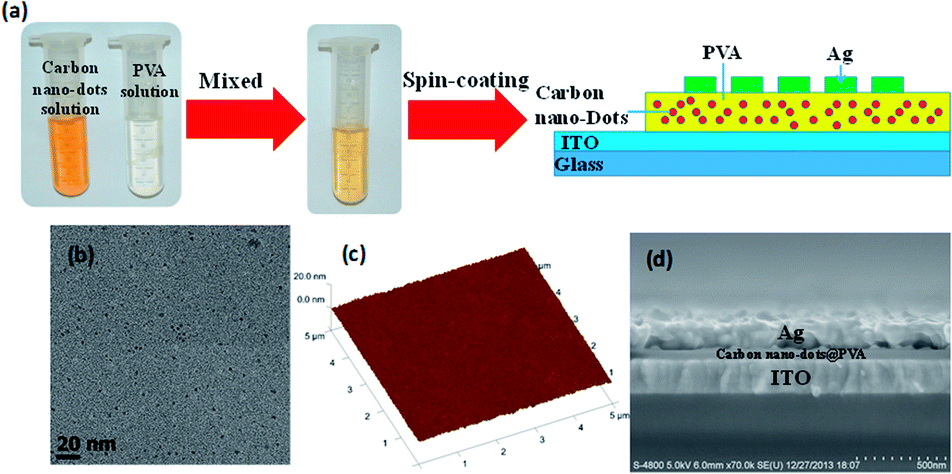 | ||
| Fig. 2 (a) Schematic diagram for the fabrication process of a carbon nano-dots-PVA composite memory devices; (b) SEM image of the film based on carbon nano-dots-PVA composite; (c) AFM images of the carbon nano-dots-PVA composite film on ITO; (d) cross-sectional SEM image of the device. | ||
To characterize the electrical bi-stable switching behavior of the devices, the electrical properties of the devices with the structure of ITO/nano-dots-PVA composites/Ag were investigated. Fig. 3(a) shows the semi-logarithmic plots of the I–V curves for the positive and negative sweeps, respectively. The arrows denote the sweeping direction of the voltage. Initially, when the diode was swept positively from 0 to 2 V, the current increased progressively with the applied bias up to about 1 V, followed by an abrupt increase of the current from 3.25 × 10⁻⁴ mA cm−2 to 297.3 mA cm−2. The switch-on voltage is much lower than the polypyrrole/PVA composites and other carbon-based materials/PVA composite memory.14,29 Further increasing the applied voltage, the high current state remained. During the second sweep from 0 to 2 V, the device was kept to be the high current state (ON-state), and no abrupt transition can be observed. These indicated the device transited from a high resistance state (OFF-state) to a low resistance state (ON-state). An ON/OFF ratio of the current up to 105 can be achieved. The transition behavior from the OFF-state to ON-state equates to the “writing” process in the digital memory devices. The device can return to the OFF-state by a suitable negative bias: a transition from high current state to the low current state can also be observed during the negative sweep from 0 to 4 V (Fig. 3(a), sweep 3), and no current transition occurs during the following voltage sweep (Fig. 3(a), sweep 4). The switching process from ON- to OFF-state is equivalent to the “erasing” process in the digital memory devices. The turn-off voltage is higher than the turn-on voltage of 1 V, approximately −3 V, which may be due to the different charge injection barriers from ITO and Ag. On account of the above switching process between ON- to OFF-state, we measure current versus voltage response of the device during write-read-erase-read voltage cycle, setting 2 V as the writing voltage, −4 V as the erasing voltage and 0.2 V as the reading voltage. Writing with 2 V bias, the device was set to ON-state, and the device can be switch off to OFF-state after erasing with −4 V bias. The switching process can be reproducible from cycle to cycle, confirming the feasibility of the nonvolatile rewritable feature of the devices, and allowing the application of carbon nano-dots–PVA composite as the active materials in the memory devices. Afterward, the data retention time and pulse voltage stresses are also investigated for the memory devices. As shown in Fig. 3(c), the programmed ON and OFF states were recorded at a reading voltage of 0.2 V after a writing/erasing process. The ON and OFF states can be preserved at the same order of magnitude, even no degradation for the duration of 3700 s, which is comparable with the organic resistive switches.30 The devices can be expected to retain the states unchanged for a longer period of time. As noticed, the ON and OFF states can be also read out under a succession of pulse bias of 0.2 V. The ON and OFF states of the devices were extremely stable even after reading up to 104 time. The excellent electrical stability ensure their potential use as a memory or switching element in organic electronics application.
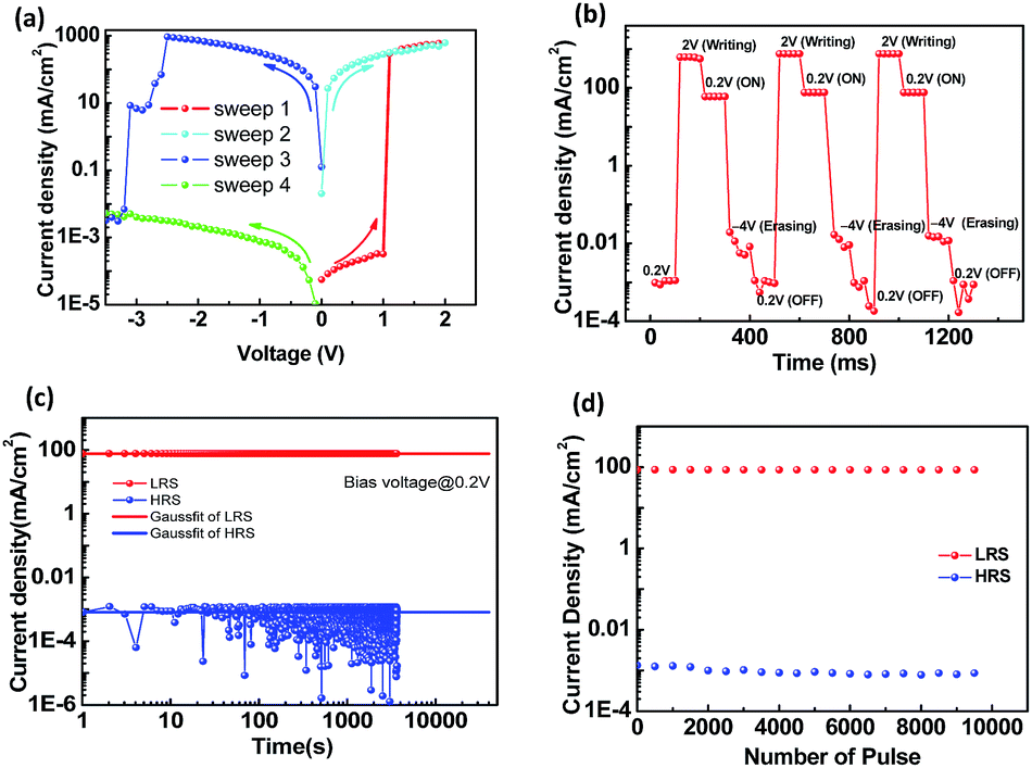 | ||
| Fig. 3 (a) The I–V characteristics of the ITO/carbon nano-dots-PVA/Ag memory devices; (b) current versus voltage response of memory devices during write-read-erase voltage cycles; (c) data retention ability of the programmed ON/OFF state at 0.2 V; (d) effect of a succession of pulses at a reading bias of 0.2 V on the device current in the written ON/OFF states. | ||
In order to understand the conduction mechanism of the carbon nano-dots-composite above, the I–V curves were analyzed with appropriate charge transport models. There are four distinct regions were observed in the I–V curves (as shown in Fig. 4(a)), indicating the different charge transport mechanism in each region. By analysis of the ln–ln plot of I versus V, a linear relationship with a slope of ∼1 for both forward and backward sweeps was observed in the LRS (region D shown in Fig.4(a)), which indicates that the conduction mechanism of the LRS is governed by Ohm's law. However, the curve in HRS was more complicated. In the region A (V < 0.6 V), ln(I) showed the linear relationship with ln(V) with the slope of 0.5, suggesting that the conduction mechanism is probably due to the thermionic emission model,31 and the charge carriers, surmounting the interface energy barriers, can be injected into the composite from the electrodes. In the region B (0.6 V < V < 0.9 V), similar linear relation was observed in the plot of ln(I)–ln(V). The slope of the fitting line increased up to 1.14, and the conduction mechanism can be described by trap-controlled space charge limited conduction (TC-SCLC). As the bias continuously increased to the threshold voltage from OFF state to ON state (about 1 V), the current increased exponentially as I vs. Vm (m = 144) in the switching region C. This correlated with the exponential distribution of trap states with in the PVA band gap. The conductive mechanism coincided with that in the MoS2 embedded PVP memory and polypyrrole nanoparticles embedded PVA memory.9,29 However, no such bistable behavior cannot be observed for the device based on PVA without carbon nano-dots (shown in Fig. S5†), experimentally supporting the key role in the bistable properties of the devices. Thus, we can conclude that the carbon nano-dots acted as carrier traps in the memory devices as we expected. These can be explained by the metal filament model. When the positive voltage is applied to the top Ag electrode, the electrochemically active Ag will be oxided to Ag+, and the mobile Ag+ will diffuse toward the ITO electrode through the active layer. The Ag metal starts to grow from the ITO and eventually form the Ag metal filament between two electrodes, leading to the Ohmic conduction in the ON-state of the memory devices.
 | ||
| Fig. 4 (a) The plot of current as a function of applied voltage for the memory devices for sweep 1 and 2; (b) experimental data and fitted lines of the I–V characteristics in Region A; (c) experimental data and fitted lines of the I–V characteristics in Region B. | ||
Fig. S6† shows the energy band diagram of the ITO/carbon nano-dots-PVA/Ag devices. The highest occupied molecular orbital (HOMO) of carbon nano-dots was −5.6 eV, determined by photoelectron spectroscopy, with a band gap of 2.28 eV. Then the lowest unoccupied molecular orbital (LUMO) can be deduced to be −3.68 eV. The HOMO and LUMO of PVA are −6.69 and −3.43 eV, respectively. This indicated that an electron-injection barrier of ∼1.4 eV, similar to that of MoS2–PVP memory devices.9 At the low bias (V < 0.6 V), the electrons will be injected into the PVA dielectric overcoming the interfacial barrier by the thermionic emission in the OFF state. The injection efficiency is low due to the large injection barrier. At the higher bias, the electrons injected will be subsequently trapped by the carbon nano-dots due to their low LUMO and quantum confinement effect. The charge transfer between PVA and carbon nano-dots followed a typical SCLC model. When the bias exceed the switching voltage, the injected carriers increase exponentially, leading to an abrupt increase of the current and the transition from the OFF state to the ON state. Consequently, almost all the traps will be occupied in the ON state, and thus the devices show the ohmic behavior. The trapped charges will be maintained in carbon nano-dots, even the device is in power off, because of the insulating property of the PVA matrix. The trapped charges can be detrapped by a reverse voltage, and then the devices return back to the OFF state. Thus, the writing and erasing process of date storage is performed.
Conclusions
Carbon nanodots has been successfully used to fabricate nano-composite nonvolatile memory devices for the first by the simple solution method with environment-friendly water as the solvent. The device with the configuration of ITO/carbon nano-dots-PVA/Ag shows the electrically bistable behavior with high ON/OFF ratio of 105 and low operation voltage: the devices can be writing/switching ON voltage at 1 V and erasing/switching OFF at negative voltage of 3 V. Both the ON and OFF states are stable for over 3400 s without any significant degradation, and the programmed states can be stable and read up to 104 cycles under a reading pulse of 0.2 V. These can be ascribed to the charge trapping and detrapping behavior of carbon nano-dots in the insulating PVA matrix under an electrical field. All these suggested the promising application potentials for the next-generation memory devices in a wide vary of commercial products.Acknowledgements
This work was financially supported by the “Hundred Talents Program” of the Chinese Academy of Sciences, the National Natural Science Foundation of China (Grant no. 61178061, no. 51373189, no. 61227008, no. 61227008 and no. 51472252), the Key Research Program of the Chinese Academy of Sciences (Grant no. KGZD-EW-T02), the Instrument Developing Project of the Chinese Academy of Sciences (Grant no. Z200929 and YZ201235), the National Basic Research Program of China (973) (No. 2014CB932600), and the Start-Up Fund of the Technical Institute of Physics and Chemistry, the Chinese Academy of Sciences.Notes and references
- J. Ouyang, C. W. Chu, C. R. Szmanda, L. Ma and Y. Yang, Nat. Mater., 2004, 3, 918 CrossRef CAS PubMed.
- B. Cho, S. Song, Y. Ji, T. W. Kim and T. Lee, Adv. Funct. Mater., 2011, 21, 2806 CrossRef CAS.
- J. C. Scott and L. D. Bozano, Adv. Mater., 2007, 19, 1452 CrossRef CAS.
- R. C. G. Naber, K. Asadi, P. W. M. Blom, D. M. de Leeuw and B. de Boer, Adv. Mater., 2010, 22, 933 CrossRef CAS PubMed.
- S. G. Hahm, N.-G. Kang, W. Kwon, K. Kim, Y.-G. Ko, S. Ahn, B.-G. Kang, T. Chang, J.-S. Lee and M. Ree, Adv. Mater., 2012, 24, 1062 CrossRef CAS PubMed.
- S.-J. Liu, P. Wang, Q. Zhao, H.-Y. Yang, J. Wong, H.-B. Sun, X.-C. Dong, W.-P. Lin and W. Huang, Adv. Mater., 2012, 24, 2901 CrossRef CAS PubMed.
- S.-T. Han, Y. Zhou and V. A. L. Roy, Adv. Mater., 2013, 25, 5425 CrossRef CAS PubMed.
- S. Cheong, Y. Kim, T. Kwon, B. J. Kim and J. Cho, Nanoscale, 2013, 5, 12356 RSC.
- J. Liu, Z. Zeng, X. Cao, G. Lu, L.-H. Wang, Q.-L. Fan, W. Huang and H. Zhang, Small, 2012, 8, 3517 CrossRef CAS PubMed.
- C.-J. Chen, C.-L. Tsai and G.-S. Liou, J. Mater. Chem. C, 2014, 2, 2842 RSC.
- W. T. Kim, J. H. Jung and T. W. Kim, Appl. Phys. Lett., 2009, 95, 0221041–0221044 Search PubMed.
- Y.-C. Lai, D.-Y. Wang, I.-S. Huang, Y.-T. Chen, Y.-H. Hsu, T.-Y. Lin, H.-F. Meng, T.-C. Chang, Y.-J. Yang, C.-C. Chen, F.-C. Hsu and Y.-F. Chen, J. Mater. Chem. C, 2013, 1, 552 RSC.
- J. Liu, Z. Yin, X. Cao, F. Zhao, L. Wang, W. Huang and H. Zhang, Adv. Mater., 2013, 25, 233 CrossRef PubMed.
- Z.-Z. Du, W. Li, W. Ai, Q. Tai, L.-H. Xie, Y. Cao, J.-Q. Liu, M.-D. Yi, H.-F. Ling, Z.-H. Li and W. Huang, RSC Adv., 2013, 3, 25788 RSC.
- Z.-L. Tseng, P.-C. Kao, M.-F. Shih, H.-H. Huang, J.-Y. Wang and S.-Y. Chu, Appl. Phys. Lett., 2010, 97, 212103 CrossRef PubMed.
- Y.-P. Sun, B. Zhou, Y. Lin, W. Wang, K. A. S. Femando, P. Pathak, M. J. Meziani, B. A. Harruff, X. Wang, H. Wang, P. G. Luo, H. Yang, M. E. Kose, B. Chen, L. M. Veca and S.-Y. Xie, J. Am. Chem. Soc., 2006, 128, 7756 CrossRef CAS PubMed.
- Y. Li, Y. Hu, Y. Zhao, G. Shi, L. Deng, Y. Hou and L. Qu, Adv. Mater., 2011, 23, 776 CrossRef CAS PubMed.
- H. Li, X. He, Z. Kang, H. Huang, Y. Liu, J. Liu, S. Lian, C. H. A. Tsang, X. Yang and S.-T. Lee, Angew. Chem., Int. Ed., 2010, 49, 4430 CrossRef CAS PubMed.
- Y. Wang, Y. Shao, D. W. Matson and Y. Lin, ACS Nano, 2010, 4, 1790 CrossRef CAS PubMed.
- C. Ding, A. Zhu and Y. Tian, Acc. Chem. Res., 2014, 47, 20 CrossRef CAS PubMed.
- F. Wang, Y. Chen, C. Liu and D. Ma, Chem. Commun., 2011, 47, 3502 RSC.
- P. Mirtchev, E. J. Henderson, N. Soheilnia, C. M. Yip and G. A. Ozin, J. Mater. Chem., 2012, 22, 1265 RSC.
- Z. Zhu, J. Ma, Z. Wang, C. Mu, Z. Fan, L. Du, Y. Bai, L. Fan, H. Yan, D. L. Phillips and S. Yang, J. Am. Chem. Soc., 2014, 136, 3760 CrossRef CAS PubMed.
- Y. Li, Y. Zhao, H. Cheng, Y. Hu, G. Shi, L. Dai and L. Qu, J. Am. Chem. Soc., 2006, 134, 15 CrossRef PubMed.
- M. Zheng, S. Liu, J. Li, D. Qu, H. Zhao, X. Guan, X. Hu, Z. Xie, X. Jing and Z. Sun, Adv. Mater., 2014, 26, 3554–3560 CrossRef CAS PubMed.
- X. L. Li, X. R. Wang, L. Zhang, S. W. Lee and H. J. Dai, Science, 2008, 319, 1229 CrossRef CAS PubMed.
- J. Ge, M. Lan, B. Zhou, W. Liu, L. Guo, H. Wang, Q. Jia, G. Niu, X. Huang, H. Zhou, X. Meng, P. Wang, C.-S. Lee, W. Zhang and X. Han, Nat. Comm., 2014, 5, 4596 CAS.
- T. López-Ríos, É. Sandré, S. Leclercq and É. Sauvain, Phys. Rev. Lett., 1996, 76, 4935 CrossRef.
- J.-Y. Hong, S. O. Jeon, J. Jang, K. Song and S. H. Kim, Org. Electron., 2013, 14, 979 CrossRef CAS PubMed.
- C. W. Lin, T. S. Pan, M. C. Chen, Y. J. Yang, Y. Tai and Y. F. Chen, Appl. Phys. Lett., 2011, 99, 023303 CrossRef PubMed.
- S. M. Sze, Physics of Semiconductor Devices, Wiley, New York, 2nd edn, 1981, p. 868 Search PubMed.
Footnote |
| † Electronic supplementary information (ESI) available: Materials and methods section, PL spectra, XPS, Raman spectra of carbon nano-dots, and absorption of carbon nano-dots film. See DOI: 10.1039/c4ra16563b |
| This journal is © The Royal Society of Chemistry 2015 |