Multifunctional reversibly sealable microfluidic devices for patterned material deposition approaches

A. Gang*a, N. Hausteina, L. Baraban*a and G. Cunibertiab
aInstitute for Materials Science and Max Bergmann Center of Biomaterials TU Dresden, 01062 Dresden, Germany. E-mail: andreas.gang@nano.tu-dresden.de; larysa.baraban@nano.tu-dresden.de
bCenter for Advancing Electronics Dresden (CfAED) TU Dresden, 01062 Dresden, Germany

Received 4th December 2014 , Accepted 9th January 2015

First published on 9th January 2015


Abstract

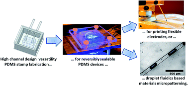
We present a concept to produce reversibly sealable polydimethylsiloxane (PDMS) based microfluidic devices with versatile channel designs, withstanding pressures up to 600 kPa. A novel fabrication strategy, namely the casting of a secondary PDMS casing around the initial channel system allows diverting the tubing attached to the channels sideways so that a simple mounting assembly can be used to press the fluidic chip onto virtually any type of substrate. We demonstrate the functionalities of the developed setup at a proof-of-concept level by direct printing of electronic interconnects onto flexible substrates in a single step. As a second application, we generate uniquely shaped polymer structures when combining the presented technique with droplet microfluidics using a UV-curable adhesive and water as continuous and dispersed phases, respectively. We believe the developed approach has a plethora of applications and a clear perspective of being used for cost-efficient and multifunctional designs of novel classes of materials and devices in diverse areas from electronics to biotechnology.


Introduction

The design of conceptually new materials that advance the understanding of biological and medical phenomena is constantly progressing.1–3 For instance in the area of tissue engineering a continuous improvement of scaffold structures with enhanced cell adhesion and growth properties is essential.4,5 Furthermore, in the field of flexible and stretchable electronics – which may facilitate e.g. conducting animal studies6 or the permanent monitoring of vital signs7,8 – new materials are required to increase device functionalities.9 In these regards, microfluidics technology emerges as a critically important tool helping to create new, exceptional materials and products by allowing the realization of novel, extraordinary fabrication strategies.10–12

Since the first introduction of a highly miniaturized gas chromatograph in 1979,13 micro- or even nanofluidic devices, in which fluids are pushed through miniature channels, gained a lot of attention from both laboratory researchers and market players, due to an efficient utilization of chemical or biological components in well-defined and confined spaces.14,15 In this manner dramatically lower sample volumes, decreased waste production and reduced human intervention can be achieved, while increasing e.g. the number of experiments running in parallel.16,17

Currently polydimethylsiloxane (PDMS) is a common material of choice when aiming for a quick prototyping of microfluidic devices as it enables an inexpensive and straightforward production of the desired channel systems.18,19 PDMS based devices have been used in a wide range of applications, such as DNA analysis,20,21 immunoassays22,23 or cell analysis,24,25 among others. For most of the assays, the PDMS cast is bonded irreversibly to the substrate by means of an oxygen plasma treatment of the respective surfaces.18 However, due to its high surface energy, a reversible adhesion of untreated PDMS to many kinds of substrates is also possible.26 This reversible adhesion is sufficiently strong to withstand fluid pressures up to 35 kPa.27 In contrast to irreversibly sealed chips,20,22–24 a reversible sealing method is favorable for a range of applications, e.g. the chemical patterning of surfaces,28 a locally confined deposition of cells,29 and the production of polymer-based microstructures via micromoulding in capillaries (MIMIC).30 To increase the applicable fluid pressures, while maintaining the reversibility of the PDMS attachment to the substrate, different techniques were developed. Le Berre et al. include in their PDMS designs, next to the fluidic circuits, channel networks that allow the application of an externally created vacuum to enhance the adhesion of the stamps to the substrates by aspiration.31 The maximum working pressure achieved in this configuration is 100 kPa, however, the space requirements of the aspiration structures may be a drawback for a number of microfluidic applications. Rafat et al. use permanent magnets to increase the maximum working pressures up to 145 kPa.32 A restriction of their approach is its suitability for simple microfluidic layouts with large channels only. Pressing the PDMS on the substrate surface using special mechanical clamps allows maximum working pressures of up to 220 kPa as demonstrated by Zang and Maeda, and Saarela et al.33 Chen et al. achieved with an glass–PDMS–glass sandwich configuration maximum working pressures of up to 400 kPa.34 However, in the latter cases33,34 the diversity of the channel designs is strongly restricted by the layout of the clamps or the glasses fixing the PDMS devices. Changing in- or out-let positions, or their amounts, respectively, would require a change of the clamp or the glass designs. Therefore, preserving high pressure resistances of reversibly sealable microfluidic systems with variable channel arrangement possibilities is of high importance, in particular for diverse biotechnological and electronic applications.

Here, we present a PDMS channel fabrication method which provides a large freedom in channel structure design, enables working pressures up to 600 kPa and keeps the channel sealing reversible, at the same time. We demonstrate at the proof-of-concept level that channel systems produced by means of the developed technique can be utilized for printing conductive poly(3,4-ethylenedioxythiophene)poly(styrenesulfonate) (PEDOT:PSS) electronic elements for flexible electronics applications. Finally, we present a process scheme how a droplet formation channel layout can be used to fix porous polymer structures with tunable pore sizes on surfaces – which may become a helpful technique to develop new scaffolds for e.g. cell growth experiments.

Materials and methods

Channel design and fabrication

Fig. 1 summarizes the production process of the newly fabricated PDMS devices. Master structures for channel casting were produced photolithographically using SU-8 photoresist (MicroChem Corp., MA, USA). PDMS base and curing agent (Sylgard® 184 Silicone Elastomer Kit, Dow Corning Corp., MI, USA) were mixed 9[thin space (1/6-em)]:[thin space (1/6-em)]1 (w/w), degassed, cast onto the mold, and cured either for 48 h at room temperature or 3 h at 60 °C (see Fig. 1A and B).18 Subsequently, holes were punched into the PDMS so that PTFE tubes (inner and outer diameters 0.5 mm and 1.0 mm, respectively) could be attached to the inlet and outlet areas of each channel (see Fig. 1C and D). For the next step (see Fig. 1E) the channel systems were pressed against a cleaned object carrier glass, and an aluminum casting frame with at least n + 1 holes (where n is the number of attached tubes) in one side was placed around them. Each tube was guided through one hole of the frame. After covering the setup with a second object carrier glass, fixing the glasses to the frame using elastic clamps and positioning the assembly in such way that the frame holes are facing upwards, a second layer of PDMS was injected and cast around the initial channel system (see also ESI, Fig. S1, left panel). A second curing step followed. PDMS stamps with up to four independent channel systems (i.e. up to eight attached tubes) were formed.
image file: c4ra15785k-f1.tif
Fig. 1 Schematic illustration of the production steps during the PDMS setup fabrication. (A–F) and a photograph of one finished and assembled device (G).

The developed approach allows diverting the utilized tubing sideways so that the resulting cuboid shaped PDMS stamp can be pressed onto virtually any kind of substrate by means of a simple aluminum sample holder combined with a Plexiglas® cover plate and four polyamide screws (see Fig. 1F and G). No chip-layout-specific holes must be considered in the clamp design which is advantageous over other reversible sealing techniques.33,34 Additionally, having large parts of the PTFE tubes (≥15 mm) embedded in the PDMS casing provides a tubing strain relief enabling a higher device robustness.

An opening in the bottom of the aluminum base allowed the observation of the fluid behavior via optical microscopy.

Leakage test

Following partially the scheme of Chen et al.34 a PDMS device with only one attached tube (see Fig. 2) was fabricated and assembled as described above. Then compressed air was pushed pressure controlled (manometer, WIKA Alexander Wiegand SE & Co. KG, Germany) into the channel while placing the entire setup inside a water bath. This allowed for investigating the maximum applicable pressure until air bubbles occurred indicating a leak.
image file: c4ra15785k-f2.tif
Fig. 2 Schematic drawing of the leakage test arrangement. Compressed air is pushed pressure controlled into a PDMS device with only one attached tube. Having the whole set-up inside a water bath allows checking for air bubbles indicating a leak.

Printing PEDOT:PSS

During the last years great attention was given to the deposition of organic conductive materials on bendable supports using different kinds of printing techniques for generating flexible electronic devices.35 Here, as a cost efficient approach to create printed electronic components on flexible substrates, an aqueous PEDOT:PSS solution (Sigma-Aldrich, MO, USA) was pushed into a two-channel-structure possessing the design, depicted in Fig. 3A. The lines between the inlet and outlet areas in position 1 and 2, and position 3 and 4, respectively are 40 μm wide and have a height of 10 μm. A printer foil supported by an object carrier glass carrier was utilized as a substrate. After fixing the PDMS on the substrate and filling the channels with PEDOT:PSS solution, at first a local heating, constricted to the aluminum base of the sample holder (see Fig. 1F) on a hot plate at 80 °C for 48 h was applied, in order to ensure the evaporation of the residual aqueous solution from the channels area. Subsequently, the whole assembly was heated in a furnace to 80 °C for another 24 h to remove any residual water from the tubing system. Afterwards, the PDMS setup was disassembled to obtain the bare printer foil with the PEDOT:PSS on top.
image file: c4ra15785k-f3.tif
Fig. 3 Layout of the channel design for printing PEDOT:PSS based flexible electronics (A). Optical microscopy images of the printer foil which was utilized as substrate before any polymer deposition (B), of the in-/out-let area (C) and one curved line section (D) after PEDOT:PSS printing. Photograph of the conductivity measurement arrangement and in the insets the simultaneously displayed data on the SMU readout and a photograph of the whole circuit, respectively (E).

Conductivity measurements, using a source measure unit (SMU, Keithley Source Meter 2604B) in combination with a micropositioner probe station, were performed to test the electrical properties of the PEDOT:PSS interconnect.

Porous polymer structure immobilization

Droplet microfluidics is utilized for the production of various kinds of spheroid-shaped objects consisting of multiple components and possessing diverse properties.10 Fig. 4A illustrates how inversed porous polymer structures can be created and immobilized on a polystyrene substrate by using a T-junction droplet formation PDMS channel layout.36 At the beginning the droplet formation is performed (t = t1, v > 0 μl s−1, see Fig. 4A). An adhesive that polymerizes under UV-irradiation (proformic 40166 – VIKO UG, Munich, Germany; UV-LED included in the adhesive kit) is utilized as continuous phase, while the droplets are composed of water (for both phases, at this stage: v = 0.003 μl min−1). After having generated a sufficient amount of droplets, so that the complete channel is filled, the flow is stopped (t > t1, v = 0 μl s−1) and droplets are immobilized by applying UV-light for at least 7 s to a desired area of the microfluidic chip. Irradiation of the entire chip is not preferred, because the consequent polymerization in the in- and out-let tubes would prevent a reutilization of the PDMS stamp. Subsequently, the setup is disassembled and the polystyrene substrate is rinsed with water and dried under nitrogen gas flow. The PDMS stamp is cleaned with acetone and isopropanol and blown dry, too. The polymer structure remaining on the polystyrene substrate is investigated via optical and scanning electron microscopy (SEM).
image file: c4ra15785k-f4.tif
Fig. 4 Schematic illustration of the droplet formation and polymer structure immobilization procedure on a polystyrene substrate using a T-junction PDMS channel layout (A). Top view optical microscopy images of the droplet formation process (B), the droplets before curing the utilized UV-curable adhesive (C), after polymerization of the adhesive and removal of the PDMS channel (D). Side view optical microscopy image of the formed polymer structure (E). SEM picture of a side view on one pore inside the polymer structure (F) and schematic drawing of a pore in the polymer material (inset in (F), orientation of the pore similar to the one in the SEM image).

Results and discussion

Leakage test

In our experiments we were able to increase the pressure of the compressed air up to 600 kPa without observing any air bubble formation in the water bath. This implies that at this pressure no leakage occurred – not between the PDMS device and the glass substrate, and also not along the PTFE tube attached to the channel. To the best of our knowledge this pressure resistance represents the highest one ever demonstrated for PDMS based reversibly sealable microfluidic devices,31–34 and it exceeds the resilience of plasma bonded PDMS-on-glass devices.37 The cuboid shape of the PDMS stamp – as a result of guiding the tubing sideways – enables a uniform pressure distribution over the entire chip when fixing it in the sample holder on the substrate via four screws. Consequently, a high device pressure resistance can be achieved. Raising the applied fluid pressure to values above 600 kPa led a leak in the outlying tubing assembly.

Comparing the achieved pressure resistance particularly to the results in the work of Saarela et al.33 in which also mechanical clamps are used, the resistance increase can be attributed to the improved tubing integration. In the work of Saarela et al.33 the tubing is only pushed into the PDMS, maximal 6 mm deep. Consequently, leakage mainly occurs at the PDMS–tubing interface. Embedding the tubing in the PDMS casing circumvents such issues.

In the initial experiments we could observe that pressing the PDMS tightly onto the substrate in some cases – particularly for wide channels (aspect ratios width/height above 10) – induces a channel collapse; a finding also reported by Xia and Whitesides.38 Therefore, in the later designs in wide channel sections additional columns were included to stabilize the structures, hence to increase the applicable pressures. The imprints of such columns can be seen in Fig. 3C.

Printing PEDOT:PSS

The results of the printing experiments using PEDOT:PSS are summarized in Fig. 3. Fig. 3A illustrates the layout of the structure, with positions 1–4 as in- or out-let tube attachment areas. The optical microscopy image in Fig. 3B shows the substrate printer foil in an untreated state. Several dark spots are visible which might be due to material inhomogeneities or surface contaminations. The optical microscopy images of an inlet region in Fig. 3C and of a curved line section in Fig. 3D illustrate that the developed printing method allows a well defined deposition of PEDOT:PSS with homogenous line widths and material densities. The conductive properties of the printed structures were examined while forcing the foil into a bent state as depicted in the photograph in Fig. 3E. Measurements between position 1 and 2, and position 3 and 4 (see Fig. 3A), respectively, showed resistivities in the low MΩ range as can be derived from the upper left inset in Fig. 3E depicting the display of the SMU during the experiment. From that one can estimate a conductivity of around 0.01 S cm−1. As the results of other groups show this value could be further enhanced.39,40 Between the positions 1 and 3 there was no conductivity. These results demonstrate that printing PEDOT:PSS based flexible electronic devices is in principle possible using the approach presented here. The 40 μm feature size achieved in our experiments are similar to the accuracies obtained with other conductive polymer printing techniques.35 Since the PDMS channel design can be changed very quickly with the presented fabrication method, a rapid prototyping of flexible electronic circuits with versatile layouts is possible.

Porous polymer structure immobilization

Fig. 4 summarizes the procedure and the outcome of the droplet formation and polymer structure immobilization experiments. As depicted in Fig. 4B water droplets are formed inside a continuous phase of UV-curable adhesive. After stopping the fluid flow (see Fig. 4C), polymerizing the adhesive and removing the PDMS channel the polymer structure is still in shape and fixed to the polystyrene substrate (see Fig. 4D). Imaging the structure from the side provides more information on the shape of the pores that the water left in its previous polymer “cage” (see Fig. 4E). The information of Fig. 4E in combination with the insights gained via SEM (see Fig. 4F) lead to the conclusion that the pores possess different kinds of walls: in the direction towards the substrate there is a thin polymer layer on the polystyrene surface; on top of the pore there is a thin closed polymer layer, as well; in two lateral directions – along the previous channel pattern – there are thick polymer walls between the separate pores; and in the other two lateral directions there are thin polymer walls with oval openings that previously allowed the water to leave the polymer structure (see also inset in Fig. 4F).

Such cavities may be very helpful for cell growth experiments. The openings at the side walls would allow the cells to enter the pores making a large surface area accessible. There are various photopolymerizable hydrogels which can be used for tissue engineering purposes and which could replace the UV-adhesive utilized in our experiments.41 By tuning the flow velocities of the different fluid phases during the experiment droplets can easily be adjusted to various sizes. In this way large amounts of differently sized pores can be produced in very short time and facilitate for example experiments on pore size dependent cell fate decisions.42

Conclusions

We developed a seminal technique to produce reversibly sealable microfluidic chips withstanding pressures up to 600 kPa. Guiding the tubes attached to the channels sideways enables a rapid prototyping of microfluidic devices with a high versatility of channel designs while no changes in the layout of the utilized mounting assembly are required. We demonstrated the potential application of such devices for fabricating flexible printed interconnects and patterned polymer microstructures.

The presented technique can be used to deposit various kinds of materials on different types of substrates opening up new possibilities for many research fields. The described method can also be of great help when a channel preparation via plasma induced bonding is not applicable, as for example in the case of using previously chemically modified substrates, or in the event of working with biological species, or when applying the MIMIC technique.

Additionally, the polymer structures periodically interspersed with cavities, created with the presented approach, could be used as photonic crystals.43 Finally, we believe that the achieved working pressures make the presented approach attractive for investigating spray-drying techniques.44

Acknowledgements

This work is funded by the European Union (ERDF) and the Free State of Saxony via the ESF project 100098212 InnoMedTec.

Notes and references

  1. N. P. King, J. B. Bale, W. Sheffler, D. E. McNamara, S. Gonen, T. Gonen, T. O. Yeates and D. Baker, Nature, 2014, 510, 103 CrossRef CAS PubMed.
  2. R. F. Service, Science, 2014, 343, 1421 CrossRef PubMed.
  3. J. A. Hubbell and R. Langer, Nat. Mater., 2013, 12, 963 CrossRef CAS PubMed.
  4. L. E. Freed, G. Vunjak-Novakovic, R. J. Biron, D. B. Eagles, D. C. Lesnoy, S. K. Barlow and R. Langer, Nat. Biotechnol., 1994, 12, 794 Search PubMed.
  5. L. Bacakova, E. Filova, M. Parizek, T. Ruml and V. Svorcik, Biotechnol. Adv., 2011, 29, 739 CrossRef CAS PubMed.
  6. A. Bozkurt and A. Lal, Sens. Actuators, A, 2011, 169, 89 CrossRef CAS.
  7. S. Bauer, Nat. Mater., 2013, 12, 871 CrossRef CAS PubMed.
  8. Y.-D. Lee and W.-Y. Chung, Sens. Actuators, B, 2009, 140, 390 CrossRef CAS.
  9. D.-H. Kim, R. Ghaffari, N. Lu and J. A. Rogers, Annu. Rev. Biomed. Eng., 2012, 14, 113 CrossRef CAS PubMed.
  10. S. S. Datta, A. Abbaspourrad, E. Amstad, J. Fan, S.-H. Kim, M. Romanowsky, H. Cheung Shum, B. Sun, A. S. Utada, M. Windbergs, S. Zhou and D. A. Weitz, Adv. Mater., 2014, 26, 2205 CrossRef CAS PubMed.
  11. Y. Yu, H. Wen, J. Ma, S. Lykkemark, H. Xu and J. Qin, Adv. Mater., 2014, 26, 2494 CrossRef CAS PubMed.
  12. S. Cheng and Z. Wu, Lab Chip, 2010, 10, 3227 RSC.
  13. S. C. Terry, J. H. Jerman and J. B. Angell, IEEE Trans. Electron Devices, 1979, 26, 1880 CrossRef.
  14. R. Fan, O. Vermesh, A. Srivastava, B. K. H. Yen, L. Qin, H. Ahmad, G. A. Kwong, C.-C. Liu, J. Gould, L. Hood and J. R. Heath, Nat. Biotechnol., 2008, 26, 1373 CrossRef CAS PubMed.
  15. D. C. Appleyard, S. C. Chapin and P. S. Doyle, Anal. Chem., 2011, 83, 193 CrossRef CAS PubMed.
  16. J. Melin and S. R. Quake, Annu. Rev. Biophys. Biomol. Struct., 2007, 36, 213 CrossRef CAS PubMed.
  17. E. K. Sackmann, A. L. Fulton and D. J. Beebe, Nature, 2014, 507, 181 CrossRef CAS PubMed.
  18. D. C. Duffy, J. C. McDonald, O. J. A. Schueller and G. M. Whitesides, Anal. Chem., 1998, 70, 4974 CrossRef CAS PubMed.
  19. E. Sollier, C. Murray, P. Maoddi and D. Di Carlo, Lab Chip, 2011, 11, 3752 RSC.
  20. C. S. Effenhauser, G. J. M. Bruin, A. Paulus and M. Ehrat, Anal. Chem., 1997, 69, 3451 CrossRef CAS PubMed.
  21. J. J. Benítez, J. Topolancik, H. C. Tian, C. B. Wallin, D. R. Latulippe, K. Szeto, P. J. Murphy, B. R. Cipriany, S. L. Levy, P. D. Soloway and H. G. Craighead, Lab Chip, 2012, 12, 4848 RSC.
  22. P. Novo, D. M. F. Prazeres, V. Chu and J. P. Conde, Lab Chip, 2011, 11, 4063 RSC.
  23. E. Eteshola and D. Leckband, Sens. Actuators, B, 2001, 72, 129 CrossRef CAS.
  24. W. Gu, X. Zhu, N. Futai, B. S. Cho and S. Takayama, Proc. Natl. Acad. Sci. U.S.A., 2004, 101, 15861 CrossRef CAS PubMed.
  25. M. Adler, M. Erickstad, E. Gutierrez and A. Groisman, Lab Chip, 2012, 12, 4835 RSC.
  26. G. T. Roman and R. T. Kennedy, J. Chromatogr. A, 2007, 1168, 170 CrossRef CAS PubMed.
  27. J. C. McDonald and G. M. Whitesides, Acc. Chem. Res., 2002, 35, 491 CrossRef CAS PubMed.
  28. E. Delamarche, A. Bernard, H. Schmid, A. Bietsch, B. Michel and H. Biebuyck, J. Am. Chem. Soc., 1998, 120, 500 CrossRef CAS.
  29. A. Khademhosseini, J. Yeh, G. Eng, J. Karp, H. Kaji, J. Borenstein, O. C. Farokhzad and R. Langer, Lab Chip, 2005, 5, 1380 RSC.
  30. E. Kim, Y. Xia and G. M. Whitesides, Nature, 1995, 376, 581 CrossRef CAS.
  31. M. Le Berre, C. Crozatier, G. V. Casquillas and Y. Chen, Microelectron. Eng., 2006, 83, 1284 CrossRef CAS.
  32. M. Rafat, D. R. Raad, A. C. Rowat and D. T. Auguste, Lab Chip, 2009, 9, 3016 RSC.
  33. V. Saarela, S. Franssila, S. Tuomikoski, S. Marttila, P. Östman, T. Sikanen, T. Kotiaho and R. Kostiainen, Sens. Actuators, B, 2006, 114, 552 CrossRef CAS.
  34. Q. Chen, G. Li, Y. Nie, S. Yao and J. Zhao, Microfluid. Nanofluid., 2014, 16, 83 CrossRef CAS.
  35. B. Weng, R. L. Shepherd, K. Crowley, A. J. Killard and G. G. Wallace, Analyst, 2010, 135, 2779 RSC.
  36. P. Garstecki, M. J. Fuerstman, H. A. Stone and G. M. Whitesides, Lab Chip, 2006, 6, 437 RSC.
  37. J. C. McDonald, D. C. Duffy, J. R. Anderson, D. T. Chiu, H. Wu, O. J. A. Schueller and G. M. Whitesides, Electrophoresis, 2000, 21, 27 CrossRef CAS PubMed.
  38. Y. Xia and G. M. Whitesides, Annu. Rev. Mater. Sci., 1998, 28, 153 CrossRef CAS.
  39. D. Alemu, H.-Y. Wei, K.-C. Ho and C.-W. Chu, Energy Environ. Sci., 2012, 5, 9662 CAS.
  40. Y. Xia and J. Ouyang, J. Mater. Chem., 2011, 21, 4927 RSC.
  41. K. T. Nguyen and J. L. West, Biomaterials, 2002, 23, 4307 CrossRef CAS PubMed.
  42. K. Franke, I. Kurth, M. Bornhäuser, C. Werner and T. Pompe, Soft Matter, 2009, 5, 3505 RSC.
  43. J. D. Joannopoulos, P. R. Villeneuve and S. Fan, Nature, 1997, 386, 143 CrossRef CAS.
  44. J. Thiele, M. Windbergs, A. R. Abate, M. Trebbin, H. Cheung Shum, S. Förster and D. A. Weitz, Lab Chip, 2011, 11, 2362 RSC.

Footnote

Electronic supplementary information (ESI) available. See DOI: 10.1039/c4ra15785k

This journal is © The Royal Society of Chemistry 2015
Click here to see how this site uses Cookies. View our privacy policy here.