Novel hybrid PVA–InZnO transparent thin films and sandwich capacitor structure by dip coating method: preparation and characterizations

Sathish Sugumarana, Chandar Shekar Bellan*b, Dinesh Muthuc, Sengodan Rajad, Dinesh Bheemane and Ranjithkumar Rajamanif
aDepartment of Physics, SVS College of Engineering, Myleripalayam, Coimbatore-642 109, India. E-mail: sathishphy@yahoo.co.in
bNanotechnology Research Lab, Department of Physics, Kongunadu Arts and Science College, G-N Mills, Coimbatore-641 029, Tamil Nadu, India. E-mail: chandar.bellan@gmail.com; Fax: +91 422 2644452
cDepartment of Physics, Bharathiar University, Coimbatore-641 046, India
dDepartment of Physics, Kumaraguru College of Technology, Coimbatore-641 049, Tamil Nadu, India
eDepartment of Biotechnology, Sree Narayanaguru College, Coimbatore-641 011, Tamil Nadu, India
fDepartment of Biotechnology, Dr N. G. P. Arts and Science College, Coimbatore-641 048, Tamil Nadu, India

Received 18th November 2014 , Accepted 5th January 2015

First published on 5th January 2015


Abstract

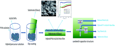
Novel hybrid poly(vinyl alcohol)–indium zinc oxide (PVA–InZnO) thin films were prepared by a simple and cost effective dip coating method and Al/PVA–InZnO/Al sandwich capacitor structure was prepared by using thermal evaporation and dip coating methods. Fourier transform infrared spectra showed the characteristic peaks correspond to metal–oxide bonds present in the films. The X-ray diffraction patterns revealed the existence of mixed phase cubic In2O3 and hexagonal wurtzite ZnO with polycrystalline structure. The scanning electron microscope images showed uniform distribution of In2O3 and ZnO nanoparticles over the entire film surface. High transmittance (50 to 80%), low absorbance, wide band gap energy (4.1 to 3.75 eV) and low α and k were obtained from an optical study. High dielectric constant, low dielectric loss and low activation energy were obtained from Al/PVA–InZnO/Al. The obtained results suggested that these prepared hybrid thin films could be used as hybrid gate dielectric layer in transparent organic thin film transistors (T-OTFT's) and in opto-electronic devices in the near future.


1. Introduction

The unique electrical and optical properties of semiconducting oxide thin films have attracted the attention of researchers worldwide because of their obvious applications in electronic and optoelectronic devices such as liquid crystal displays, solar cells, light emitting devices and switching devices.1–5 Among semiconducting oxides, transparent conductive oxides (TCOs) have been touted as the natural successor materials for microelectronic devices, which offer great properties for the most efficient and cost effective utilization of a wide variety of applications. TCOs have many advantages compared to silicon or organic semiconductors. TCOs are transparent in the visible region due to their large band gap energy, environmental stability and high mobility. Indium oxide (In2O3) and zinc oxide (ZnO) have been considered as TCOs for many years. In2O3 is a n-type semiconductor with a wide optical band gap (3.7 eV), which is a very important material for micro and opto-electronic applications due to high electrical conductivity, high transparency in the visible light range, high reflectivity in the infrared (IR) light range and high refractive index, n > 1.8.6 ZnO has been investigated in recent years because of its good electrical and optical properties with large band gap of 3.3 eV, abundant in nature and lack of toxicity.7 Presently In2O3 and ZnO based TCOs such as indium zinc oxide (IZO), indium–gallium oxide (IGO) and indium–gallium–zinc oxide (IGZO) materials have been used as channel layer for thin film transistor (TFT) fabrications.8 There are many techniques available for preparation of In2O3, ZnO, IZO, IGO, IGZO and zinc tin oxide (ZTO) thin films for transparent active-channel materials in TTFTs9–16 and solar cells.17–19 So far there is no report on preparation and characterization of hybrid thin film based on IZO or InZnO.

Hybrid/composite thin films are being considered as a group of new class of advance materials and promises number of applications.20,21 A hybrid material consists of soluble polymers with excellent electrical, optical, mechanical properties and nice film formation can be used in electronic devices, gas sensors, large area flat panel displays and to make polymer light-emitting diodes.22–24 Recently, significant interest has been shown to prepare thin films based on polymeric–inorganic materials due to their physical and chemical properties and many potential applications in electronic and opto-electronic devices.25–27 In our previous work, we have reported on the characterization of virgin poly(vinyl alcohol) PVA, hybrid PVA–InAlO, nanocomposite PVA–In2O3 and PVA–TiO2 thin films prepared by dip coating method.28–31 To the best of our knowledge, there is no work reported in literature on poly(vinyl alcohol)–indium zinc oxide (PVA–InZnO) thin films. An attempt has been made to prepare hybrid PVA–InZnO thin films by a simple dip coating method and to study their structure, morphology, optical and dielectric properties in the present work.

2. Experimental technique

2.1. Materials

Commercially available PVA (poly(vinyl alcohol)), indium oxide (In2O3) and zinc oxide (ZnO) were purchased from Sigma Aldrich and Nice Chemicals Pvt. Ltd, India. 1 mm thickness of micro slides (glass plates) was purchased from Precision Scientific Co. (CBE), India.

2.2. Preparation of hybrid precursor solution

Initially 50 ml of PVA solution (0.5 g of PVA in 50 ml) was prepared by dissolving PVA in deionized water by magnetic stirring at 80 °C for 5 h. An equimolar ratio (1[thin space (1/6-em)]:[thin space (1/6-em)]1) of In2O3 and ZnO were mixed into PVA solution. The mixed solution was magnetically stirred until gel-precipitation is formed. Then the gel-precipitation was ultrasonically churned in a water bath for 10 minutes. During the ultrasonication, the metal oxides collide to form a bond of continuous network that was followed by centrifugal washing at 6000 rpm for 10 minutes. The continuous ultrasonication and centrifugal washing process was repeated for 5 times to get well dispersed hybrid precursor solution.

2.3. Preparation of hybrid PVA–InZnO thin films

The pre-cleaned glass plates were dipped into the hybrid precursor solutions for 5 minutes at room temperature to get hybrid thin films (PVA–InZnO). The as deposited hybrid thin film and film annealed at 50 °C, 100 °C and 150 °C for 1 h were used to study structure, morphology, optical and dielectric properties. Sandwich capacitor structure (Al/hybrid film/Al) was fabricated to study the dielectric and conduction behaviour. Initially, aluminum base electrode of about 180 nm thickness was deposited over the pre-cleaned glass substrate by thermal evaporation technique (pressure of 10−5 Torr) using suitable masks. The middle hybrid film was deposited above the bottom electrode by dip coating method. Finally the top electrode of about 180 nm was deposited above the hybrid film by thermal evaporation technique using suitable masks to complete the Al/PVA–InZnO/Al sandwich capacitor structure. The preparation route with schematic diagram of (a) hybrid thin film and (b) sandwich capacitor structure are shown in Fig. 1a and b.
image file: c4ra14817g-f1.tif
Fig. 1 (a) Hybrid PVA/InZnO thin film and (b) sandwich capacitor structure (Al/PVA–InZnO/Al).

2.4. Characterization

2.4.1. Fourier transform infrared (FTIR) studies. The functional groups present in the hybrid thin films were identified by Thermo Nicolet, Avatar 370 FTIR spectroscopy with a spectral range of 4000–400 cm−1 and resolution of 4 cm−1.
2.4.2. X-ray diffraction (XRD) analysis. The structure of the hybrid thin films was analyzed by using X-ray diffraction (XRD) analysis using Bruker AXS D8 advance diffractometer having CuKα (λ = 1.5406 Å) radiation with value of 2θ ranged from 20° to 80°, operating voltage of 40 kV and a current of 30 mA.
2.4.3. Scanning electron microscopy (SEM-EDS) analysis. The surface morphology was studied by using JEOL Model JSM-6390LV scanning electron microscopy (SEM). The elemental composition of films was determined using the JEOL Model JED-2300 energy dispersive X-ray analysis (EDS).
2.4.4. UV-visible-NIR spectrophotometer. The optical properties were studied for the wavelength range of 200 nm to 2500 nm with a resolution of 0.1 nm by using a UV-Vis-NIR (JASCO V-670, Japan) spectrophotometer.
2.4.5. Dielectric study. The dielectric properties were carried out on sandwich capacitor structure of Al/PVA–InZnO/Al by using Agilent 4284(A) precision LCR meter for constant voltage range of 10 mVrms to 1 Vrms and 10 Amps operating current for the frequency and temperature range between of 1 kHz to 1 MHz and 30 °C to 150 °C respectively.

3. Results and discussion

3.1. FT-IR analysis

Fig. 2 shows the FTIR spectrum of hybrid PVA–InZnO thin films. FTIR spectra of as deposited and annealed hybrid thin films show a relatively broad and intense absorption band at around 3400 cm−1 indicating the presence of polymeric association of the free hydroxyl groups and bonded OH stretching vibrations (In–OH and Zn–OH).31–33 It indicates the existence of hydrogen bonding between polymer matrix and metal oxide nanoparticles and the shift of the peaks upon annealing temperature may be due to weakened or redistribution of hydrogen bonds in the material.34 The C–H stretching bands observed at around 2900 cm−1 and the bands at around 1600 cm−1 to 1750 cm−1 is attribute to the moisture in the film.29 The symmetric bending mode γδ(CH2) and CH2 rocking characteristics of PVA are found at 1435 cm−1 and 1413–1441 cm−1 respectively.35 The band at around 1327 cm−1 is assigned to the wagging vibration of CH2 whereas bands at about 1090 cm−1 is assigned to γ(C–O) stretching vibration.32 The C–O–C stretching and CH2 bending are respectively observed at around 1100 cm−1 and 850 cm−1.36 The observed bands in the 400–800 cm−1 region is due to the crystallites of metal oxides embedded in the polymer matrix.36–38 The observed absorption peaks at 424, 538, 585 and 602 cm−1 for as deposited and 426, 538, 565 and 603 cm−1 for annealed films may be attributed to the characteristic of metal–oxide bond present in the films.27,39–42
image file: c4ra14817g-f2.tif
Fig. 2 FTIR spectra of as deposited and annealed hybrid PVA–InZnO thin films.

3.2. X-ray diffraction analysis

The XRD pattern of as deposited and annealed hybrid PVA–InZnO thin films are shown in Fig. 3. A broad hump observed at 2θ = 20–30° for as deposited and film annealed at 50 °C is due to diffuse scattering of amorphous PVA, whereas the width and intensity of the broad hump decreases with increase of annealing temperature (100 °C and 150 °C). XRD pattern exhibits predominant diffraction peaks at around 2θ = 30° and 31°, which corresponds to the mixed phase of polycrystallinity with cubic In2O3 and hexagonal wurtzite ZnO structure.13,15,43 The observed diffraction peaks at 2θ values of 30, 35, 51 and 56° respectively corresponds to (222), (400), (440) and (622) planes may be due to cubic In2O3 and the peaks at 31, 34, 57, 61 and 68° respectively corresponds to (100), (002), (110), (103) and (112) planes may be due to hexagonal wurtzite ZnO.27,41,44–47 The obtained diffraction peaks are consistent with the standard data for cubic In2O3 (JCPDS-06-0416) and hexagonal wurtzite ZnO (JCPDS-36-1451). It is clearly evident that there is no phase change upon annealing. Similarly, no characteristic peaks due to impurities or complex phases other than cubic In2O3 and hexagonal wurtzite ZnO were detected. This explains the homogeneous crystal nature of hybrid PVA–InZnO thin films. From the Fig. 3, it is seen that the diffraction peak intensity increases with increase of annealing temperature, because annealing temperature provide sufficient energy to crystallites and to orient in proper equilibrium sites, which leads to increase in intensity.48 It clearly indicates that there is an improvement in crystallinity with increase of annealing temperature.19 The observed high intensive narrow diffraction peaks indicate crystalline nature of the films.
image file: c4ra14817g-f3.tif
Fig. 3 XRD patterns of as deposited and annealed hybrid PVA–InZnO thin films.

3.3. Morphological analysis

The SEM images of as deposited and annealed hybrid PVA–InZnO thin films are shown in Fig. 4. SEM images of as deposited and annealed films revealed very different morphologies. The smooth layer mainly consists of polymer while, the inferior ones (bright spot) are truly hybrid materials, with a high content of mineral phase of indium oxide and zinc oxide. It is seen that In2O3 and ZnO nanoparticles are uniformly distributed over polymer matrix and there is no cracks, pits and pinholes are seen on the surface.49 It indicates maximum homogeneous pattern, particles are well bonded with polymer matrix and approximately there is no differentiation between In2O3 and ZnO particles on film surface.24,50,51 It indicates that metal oxide nanoparticles are homogeneously distributed in polymer matrix, which is responsible for high transparency of the film.34 SEM images of as deposited film revealed homogeneous with uniform distribution of grains whereas agglomerated grains observed for films annealed at 50 °C, 100 °C and 150 °C respectively. It indicates that morphology of the film is affected by annealing temperature. The observed homogeneous dispersion of metal oxide nanoparticles in polymer matrix is in good agreement with recently reported work in literature.52 The size of the grain increases with increase of annealing temperature. Increase in grain size upon annealing leads to decrease of grain boundary scattering. It is clear that preparation of smooth surface with transparent hybrid thin film is possible by the addition of metal oxides in polymer matrix using a dip coating method. The obtained smooth surface having grain size in the micrometer scale range for as deposited and annealed hybrid thin films indicated the feasibility of utilizing them in gas sensor and other applications due to their high specific surface area and excellent channels for charge transmission.24,41,45,53–56 Fig. 5 shows the EDS spectrum of hybrid PVA–InZnO thin films. It reveals the presence of elements such as In, Zn and O in both as deposited and annealed hybrid thin films.47 The variation of atomic percentage of elements with annealing temperature are given in Table 1. The Table 1 shows that the atomic percentages of elements in the hybrid thin films were affected by annealing temperature.
image file: c4ra14817g-f4.tif
Fig. 4 SEM image of as deposited and annealed hybrid PVA–InZnO thin films.

image file: c4ra14817g-f5.tif
Fig. 5 EDS spectra of as deposited and annealed hybrid PVA–InZnO thin films.
Table 1 Atomic % of In, Zn and O
Hybrid thin film Atomic %
In Zn O
As deposited 55.72 21.9 22.38
50 °C 50.04 29.37 20.59
100 °C 52.39 27.67 19.94
150 °C 60.54 22.44 17.02


3.4. UV-visible-NIR spectroscopy

Fig. 6a and b shows the UV-Vis transmittance and absorbance spectra of as deposited and annealed hybrid PVA–InZnO thin films. As deposited film showed maximum transmittance of 50% whereas annealed films showed maximum transmittance of 51%, 53% and 80% for 50 °C, 100 °C and 150 °C respectively. It is seen that transmittance increases with increase of annealing temperature. Almost 80% of transmittance is obtained for films annealed at 150 °C. Low transmittance observed in the lower wavelength range and it increases toward increase in the higher wavelength range.42,57 The observed decrease in transmittance in the lower wavelength range may be due to band gap absorption of metal oxide semiconductors in polymer matrix. It is well known that the change in optical transmission with annealing temperature may be due to the decrease in number of defects, increase of crystallite size, decrease in film thickness and improvement in surface morphology of the respective films. The observed increase of optical transparency upon annealing temperature could be attributed to the formation of high crystallinity and smooth surface with less defect states resulted in decrease of optical scattering. The observed transmittance values are in good agreement with early reported work on hybrid/composite thin films based on In2O3, ZnO and TiO2.6,46,58,59 The obtained high transmittance in the entire visible to infrared wavelength ranges are close to the reported value of transmittance for conventional glass substrate in literature.60 Very low transmittance in the range between 290 nm and 340 nm indicates that these hybrid thin films could be used for UV-blocking contact lens.61 High transparency in the visible region is essential for window layer in solar cells whereas high transparency in the NIR region exhibited by these thin films makes them good materials for the construction of poultry roofs and walls. This has the potential to minimize the cost of energy consumption associated with the use of electric bulbs, heater, stove and the hazards associated with them, while at the same time protecting the chicks from UV radiation.62 Fig. 6b shows the absorption spectra of hybrid PVA–InZnO thin films. The observed change in optical absorption is due to annealing effect which leads to decrease in optical absorption with increase of annealing temperature. It is also seen that the absorption is very high in the UV region whereas very low in the visible to NIR region for both as deposited and annealed films.9 Hybrid thin films exhibit very low absorption as well as high transmittance, which could be used for antireflection coatings in solar devices.
image file: c4ra14817g-f6.tif
Fig. 6 (a) Transmittance and (b) absorbance versus wavelength of hybrid PVA–InZnO thin films.

The band gap energy (Eg) of the films can be estimated by extrapolating the linear part of the (αhν)2 versus hν plot to the x-axis (Tauc's plot), which is shown in Fig. 7. The estimated band gap energy values are 4.1 eV, 3.99 eV, 3.98 eV and 3.75 eV for as deposited and film annealed at 50 °C, 100 °C and 150 °C respectively. The obtained wide optical band gap energy values are in good agreement with early reported work on virgin In2O3/ZnO, hybrid In2O3/TiO2 and indium zinc oxide based thin films.6,58,63–65 From the Fig. 7, it is seen that the band gap energy value decreases with increase of annealing temperature. The observed decrease in band gap energy with increase of annealing temperature is in good agreement with the band gap energy values reported in literature for virgin PVA and their doped films.66 This is possibly due to the many factors, such as (i) decrease in the number of defects (ii) evaporation of water molecules off the film (iii) decrease in density of localized states (iv) reorganization of the films62 (iv) decrease in oxygen content (v) increase in grain boundary growth and (vi) shift in the band gap energy due to increasing order of dielectric constant (because dielectric constant is inversely proportional to its band gap energy) with annealing temperature. The observed less transmittance for as deposited film as compared to annealed films may be due to increase in grain size and decrease in band gap energy with increase in annealing temperature. The high transmittance (≈80%) with wide band gap obtained for hybrid thin films are comparable with the transmittance and band gap values reported for PVA based composite thin films prepared by various methods.10,65–70 The obtained high transmittance and low absorption with wide band gap indicates the feasibility of using these new hybrid thin films in many optoelectronic devices.


image file: c4ra14817g-f7.tif
Fig. 7 (αhν)2 versus energy () for hybrid PVA–InZnO thin films.

The optical constants such as absorption coefficient (α) and extinction coefficient (k) of hybrid thin films were evaluated from optical transmission spectra by using Swanepoel method.71 The absorption coefficient (α) of these materials strongly depends on optical transmission (T), wavelength (λ) and thickness of the film (d). The absorbance coefficient gives information about the band gap of the materials, which is extremely important for understanding the electrical properties of semiconductor and is therefore of great practical interest.72 Fig. 8a shows the absorption coefficient (α) versus wavelength. Very low values of α were obtained for the entire visible and NIR region and further it decreases with increase of annealing temperature. The absorbance coefficient α > 104 cm−1 suggests the occurrence of direct optical transition. The extinction coefficient (k) and refractive index (n) are important parameters characterizing photonic materials.69 The variation of extinction coefficient (k) as a function of wavelength for different temperatures is shown in Fig. 8b. From the plot it is seen that the k value increases with increase of wavelength, which is due to interband transition between the valance and conduction bands.73–75 It is also seen that the k values are decreasing with increase of annealing temperature. This is possibly due to the improvement in the crystallinity with increase in annealing temperature, which leads to minimum imperfection. The low values of k are 0.03 to 0.05 in the lower wavelength range whereas it is 0.05 to 0.3 in the higher wavelength range respectively for both as deposited and annealed hybrid thin films. Generally, the high value of k is due to lack of smooth surface with annealing temperature, which leads to little surface optical scattering and optical loss. But in this case, the hybrid thin films show a decrease of k value with increase of annealing temperature. The obtained k value is high for as deposited film and it further decreases with increase of annealing temperature. Very low values of k obtained for films annealed at 150 °C. The obtained low value of k implies that fraction of light loss due to scattering for both as deposited and annealed films which indicates that the prepared hybrid thin films have very low absorption.76 The observed decrease of k with increase of annealing temperature may also be due to the decrease in thickness of the film with increase of annealing temperature.77,78 The obtained values of optical transmittance, low absorption, wide band gap energy and optical constants such as wavelength dependence of α and k values are in good accordance with the early reported work in literature.79 The optical studies suggests that the optical properties of hybrid thin films are significantly affected by annealing temperature due to the improvement of the crystallinity of the hybrid films with increase of annealing temperature.58


image file: c4ra14817g-f8.tif
Fig. 8 (a) absorption coefficient (α) and (b) extinction coefficient (k) versus wavelength of hybrid PVA–InZnO thin films.

3.5. Dielectric study

Fig. 9a and b shows the frequency and temperature dependence of capacitance for hybrid PVA–InZnO thin films. It is seen that the capacitance value decreases with increase of frequency and it increases with increase of temperature (Fig. 9a). The large increase in capacitance towards the low frequency region may be attributed to the blocking of charge carriers at the electrodes. Actually, the charge carriers present in the film migrate upon the application of the field and because of the impedance to their motion at electrodes resulted in space charge layer which leads to a large increase in the capacitance at low frequencies. The observed decrease of capacitance with increasing frequency is also attributed to the increasing inability of the dipoles to orient themselves in a rapidly varying electric field and slow release of charge carriers from relatively deep traps. It is seen that the capacitance decreases in the low frequency range and attains a constant value in the high frequency range for the temperature ranges studied, which is the usual behavior observed in many dielectric films.80 Fig. 9b shows that low value of capacitance obtained for lower temperature region where as it is very high for higher temperature region.81 This is the general capacitance behavior normally observed for dielectric materials. The observed capacitance values are ranging between 63 and 218 nF. The hybrid PVA–InZnO thin film exhibited higher capacitance value as compared to the capacitance values reported for virgin PVA thin films in the literature.37,82–85
image file: c4ra14817g-f9.tif
Fig. 9 (a and b) Frequency and temperature dependence of capacitance of hybrid PVA–InZnO thin films.

Fig. 10a and b shows the frequency and temperature dependence of dielectric constant (ε′) of hybrid PVA–InZnO thin films. It is seen from the Fig. 10a, that the ε′ decreases with increase of frequency of an applied field for all the temperature ranges studied. High ε′ is obtained at lower frequency range and it decreases with increase of applied frequency. Similar frequency dependence ε′ was reported by Roy et al.86 The decrease in the values of ε′ with increase of frequency can be related to the electron exchange interaction between In and Zn ions which cannot follow the alternation of the electric field beyond a certain frequency. The observed decrease of ε′ with increase of frequency may also be due to the inability of dipoles to orient themselves in the direction of the applied field. Similar trend has been reported for PVA based composite thin film by Seoudi et al.87 The observed results are in good agreement with Koop's phenomenological theory.88 The obtained high ε′ at low frequency region may be due to the presence of polarization mechanisms like, space charge, orientation, electronic and ionic polarization, whereas the low values of ε′ at higher frequency may be due to the loss of significance of these polarizations gradually.88,89


image file: c4ra14817g-f10.tif
Fig. 10 (a and b) Frequency and temperature dependence of dielectric constant of hybrid PVA–InZnO thin films.

From the Fig. 10b, it is seen that the ε′ increases with increase of temperature for a given frequency range. The observed very low values of ε′ at lower temperature region are due to frozen of molecular dipoles. The observed increase in ε′ with increase of temperature is due to more rotational freedom of dipoles by thermal activation.90 It is well known that the significant change in dielectric constant with increase in temperature is attributed to many factors such as development of space charges, mobility of ionic carriers and polarization effect. The high dielectric constant value obtained at high temperature regions may be due to the interfacial orientation and space charge polarization effect,91 which results in increase of total polarization arising from dipoles and trapped charge carriers. The ε′ value varies from 5 to 18. The obtained ε′ value is very high as compared to ε′ values reported for virgin PVA thin film and PVA based composite thin films due to In2O3 and ZnO nanoparticles embedded in the polymer matrix.29,87,92,93 The obtained ε′ values are reasonably good enough to use them as dielectric layer in device applications.94

The temperature coefficient of capacitance (TCC) is an important parameter for accessing the expected behavior in thin film circuits. The growing interest in the choice of material for application as capacitor suggests that the temperature coefficient of capacitance (TCC) and temperature coefficient of permittivity or dielectrics (TCP) is to be investigated thoroughly. According to Chandar Shekar et al.82 and Deger et al.95 the TCC, TCP and linear expansion coefficient (α) of hybrid thin films have been determined from the capacitance versus temperature, dielectric constant versus temperature plots and the estimated values are presented in the Table 2.

Table 2 TCC, TCP and α values of hybrid PVA–InZnO thin films
Frequency TCC × 103 (ppm K−1) TCP × 103 (ppm K−1) α × 103 (ppm K−1)
1 kHz 3.76306 3.76108 0.00198
10 kHz 4.08173 4.07970 0.00203
100 kHz 3.96590 3.96382 0.00208
1 MHz 2.64869 2.64770 0.00099


The frequency and temperature dependence of dielectric loss for hybrid PVA–InZnO thin film is shown in Fig. 11a and b. From the figures it is seen that the dielectric loss decreases with increase of frequency whereas it increases with increase of temperature. The loss is high at low frequency region due to high resistivity which requires more energy for electron exchange between the ions and the loss is very low at high frequency region due to low resistivity which requires low energy for electron transfer between the ions. The low loss values at higher frequencies show the potential of hybrid thin film for high frequency applications. The obtained decreasing nature of dielectric loss with increasing frequency may also be due to the deduction of chain movement of the polymer through physical bonding or through confinement by the presence of In2O3 and ZnO nanoparticles. These plots suggest that the dielectric loss of prepared hybrid thin films strongly depends on the frequency of the applied field. The relative high value of dielectric loss for lower frequency ranges is due to dipole polarization. As the frequency increases the dipole polarization effect will tend to zero and the dielectric loss factor depends only on the electronic polarization. The observed increase of dielectric loss with increase of temperature (30 °C to 150 °C) for the all frequency ranges may also be due to increase in density of the dipole orientation.96 The dielectric loss increases with increase of temperature, proving a thermally-activated loss mechanism. The magnitude of the loss factor increases with increase in temperature before the attainment of glass transition temperature.97


image file: c4ra14817g-f11.tif
Fig. 11 (a and b) Frequency and temperature dependence of dielectric loss of hybrid InZnO thin films.

The double logarithmic plot of the dependence of AC conduction on frequency for different temperatures is shown in Fig. 12a. It is seen that the AC conductivity increases with increase of frequency for all temperature ranges studied. It is seen that the AC conductivity changes in accordance with the relation, σac α ωn, where n depends on the frequency and temperature. Apart from frequency and temperature, the high AC conductivity may also be due to protonation and crystallinity of the films.98 The increase of AC conductivity with frequency observed for the hybrid films may also be due to the hopping of electrons between the charge carriers (In and Zn).99,100 The observed trend indicates the normal dielectric behavior of the prepared hybrid thin films. Arrhenius plot between log[thin space (1/6-em)]σ versus 1000/T is drawn (Fig. 12b) to evaluate activation energy and the calculated activation energy values are given in Table 3. The calculated activation energy values are very low for various frequency ranges studied. The obtained low values of activation energy indicate that the conduction in the hybrid film may be due to electrons rather than ions. The observed optical and dielectric properties of the hybrid PVA–InZnO thin film are in good agreement with earlier reported work on other oxide materials.31,101–103 The obtained optical and dielectric properties of the dip coated hybrid PVA–InZnO thin films are good enough to be used in optical devices and as high dielectric layer in organic thin film transistors.


image file: c4ra14817g-f12.tif
Fig. 12 (a and b) Log[thin space (1/6-em)]σ versus log[thin space (1/6-em)]f and log[thin space (1/6-em)]σ versus 1000/T for different temperatures and frequencies of hybrid PVA–InZnO thin films.
Table 3 Activation energy values of hybrid PVA–InZnO thin films
Frequency Activation energy × 10−4 (eV)
1 kHz 1.74
10 kHz 0.96
100 kHz 0.53
1 MHz 0.38


4. Conclusion

Novel hybrid PVA–InZnO thin film and sandwich capacitor structure were prepared by a simple dip coating method. The presence of metal–oxide bond and elements (In, Zn and O) in the hybrid thin films were confirmed from FTIR and EDS analysis. The XRD patterns revealed mixed phase of cubic In2O3 and hexagonal wertzite ZnO with polycrystalline structure. SEM images showed uniform distribution of particles over the entire film surface. The optical analysis showed higher transmittance (50% to 80%), wide band gap energy (4.1 eV to 3.75 eV) and low values of α and k. The dielectric study showed high dielectric constant (5 to 18) and low values of dielectric loss, TCC, TCP, α and activation energy. The prepared material of polycrystalline structure, smooth surface, low absorption, excellent transparency, wide band gap energy and good dielectric behavior suggested that the prepared hybrid PVA–InZnO thin films could be used in various electronic and opto-electronic devices in near future.

Acknowledgements

One of the authors S. Sathish gratefully acknowledges Jawaharlal Nehru Memorial Fund (JNMF), New Delhi, India, for financial support to this research work under JNMF Scholarship for doctoral studies. Authors are expressing their sincere thanks to Kongunadu Arts and Science College and CUSAT-STIC, India for their technical support.

References

  1. G. Kiriakidis, N. Katsarakis, M. Bender, E. Gagaoudakis and V. Cimalla, Mater. Phys. Mech., 2000, 1, 83–97 CAS.
  2. C. Grivas, S. Mailis, L. Boutsikaris, D. S. Gill, N. A. Vainos and P. J. Chandler, Laser Phys., 1998, 8, 326–330 CAS.
  3. T. Dedova, M. Krunks, M. Grossberg, O. Volobujeva and I. Oja Acik, Superlattices Microstruct., 2007, 42, 444–450 CrossRef CAS PubMed.
  4. F. K. Allah, S. Y. Abe, C. M. Nunez, A. Khelil, L. Cattin, M. Morsli, J. C. Bernede, A. Bougrine, M. A. del Valle and F. R. Diaz, Appl. Surf. Sci., 2007, 253, 9241–9247 CrossRef CAS PubMed.
  5. S. Calnan and A. N. Tiwari, Thin Solid Films, 2010, 518, 1839–1849 CrossRef CAS PubMed.
  6. J. L. Vossen, Phys. Thin Films, 1977, 9, 1 CAS.
  7. C. F. Yu, C. W. Sung, S. H. Chen and S. J. Sun, Appl. Surf. Sci., 2009, 256, 792–796 CrossRef CAS PubMed.
  8. K. Ebata, S. Tomai, Y. Tsuruma, T. Litsuka, S. Matsuzaki and K. Yano, Appl. Phys. Express, 2012, 5, 011102 CrossRef.
  9. K. Makise, N. Kokubo, S. Takada, T. Yamaguti, S. Ogura, K. Yamada, B. Shinozaki, K. Yano, K. Inoue and H. Nakamura, Sci. Technol. Adv. Mater., 2008, 9, 044208 CrossRef.
  10. E. M. C. Frotunato, P. M. C. Barquinha, A. C. M. B. G. Pi Goncalves, A. J. S. Marques, L. M. N. Pereira and R. F. P. Martins, Adv. Mater., 2005, 17, 590–594 CrossRef.
  11. H. Q. Chiang, J. F. Wager, R. L. Hoffman, J. Jeong and D. A. Keszler, Appl. Phys. Lett., 2005, 86, 013503 CrossRef PubMed.
  12. B. Yaglioglu, H. Y. Yeom, R. Beresford and D. C. Paine, Appl. Phys. Lett., 2006, 89, 062103 CrossRef PubMed.
  13. K. Nomura, T. Kamiya, H. Ohta, K. Ueda, M. Hirano and H. Hosono, Appl. Phys. Lett., 2004, 85, 1993–1995 CrossRef CAS PubMed.
  14. K. Nomura, A. Takagi, T. Kamiya, H. Ohta, M. Hirano and H. Hosono, Jpn. J. Appl. Phys., 2006, 45, 4303–4308 CrossRef CAS.
  15. C. G. Choi, S. J. Seo and B. S. Bae, Electrochem. Solid-State Lett., 2008, 11, H7–H9 CrossRef CAS PubMed.
  16. M. G. Mcdowell and I. G. Hill, IEEE Trans. Electron Devices, 2009, 56, 343–347 CrossRef CAS.
  17. W. K. Lin, K. C. Liu, S. T. B. Chang and C. S. Li, Thin Solid Films, 2012, 520, 3079–3083 CrossRef CAS PubMed.
  18. Y. B. Xiao, S. M. Kong, E. H. Kim and C. W. Chung, Sol. Energy Mater. Sol. Cells, 2011, 95, 264–269 CrossRef CAS PubMed.
  19. A. Olziersky, A. Vila and J. R. Morante, Thin Solid Films, 2011, 520, 1334–1340 CrossRef CAS PubMed.
  20. A. Singhal, K. A. Dubey, Y. K. Bhardwaj, D. Jain, S. Choudhury and A. K. Tyagi, RSC Adv., 2013, 3, 20913–20921 RSC.
  21. A. Lagashetty, S. Basavaraj, M. Bedre and A. Venkatarman, J. Metall. Mater. Sci., 2009, 51, 297–306 CAS.
  22. S. Gupta, S. Sindhu, K. Arul Varman, P. C. Ramamurthy and G. Madras, RSC Adv., 2012, 2, 11536–11543 RSC.
  23. Q. H. Chen, S. Y. Shi and W. G. Zhang, Colloid Polym. Sci., 2009, 287, 533–540 CAS.
  24. A. Singhal, M. Kaur, K. A. Dubey, Y. K. Bhardwaj, D. Jain, C. G. S. Pillai and A. K. Tyagi, RSC Adv., 2012, 2, 7180–7189 RSC.
  25. V. A. Bershtein, V. M. Gun'ko, L. M. Egorova, Z. Wang, M. Illsley, E. F. Voronin, G. P. Prikhod'ko, P. N. Yakushev, R. Leboda, J. Skubiszewska-Zięba and S. V. Mikhalovsky, RSC Adv., 2012, 2, 1424–1431 RSC.
  26. H. L. Tai, Y. D. Jiang and G. Z. Xie, J. Electron. Sci. Technol., 2010, 8, 154–159 CAS.
  27. N. Bouropoulos, G. C. Psarras, N. Moustakas, A. Chrissanthopoulos and S. Baskoutas, Phys. Status Solidi A, 2008, 205, 2033–2037 CrossRef CAS.
  28. S. Sathish, B. Chander Shekar and B. T. Bhavyasree, Adv. Mater. Res., 2013, 678, 335–342 CrossRef.
  29. S. Sathish, M. Dinesh and B. Chandar Shekar, Int. J. Adv. Mater. Sci., 2013, 4, 93–100 Search PubMed.
  30. S. Sathish, B. Chandar Shekar and R. Sathyamoorthy, Phys. Procedia, 2013, 49, 160–170 CrossRef PubMed.
  31. S. Sathish, B. Chandar Shekar and N. Manivannan, Int. J. Polym. Anal. Charact., 2014, 19, 549–561 CrossRef.
  32. M. Tsukada, G. Freddi and J. S. Crighton, J. Polym. Sci., Part B: Polym. Phys., 1994, 32, 243–248 CrossRef.
  33. P. Sakellariou, A. Hassan and R. C. Rowe, Polymer, 1993, 34, 1240–1248 CrossRef CAS.
  34. Y. Hu, G. Gu, S. Zhou and L. Wu, Polymer, 2011, 52, 1222–1229 Search PubMed.
  35. J. Junkasem, R. Rujiravanit and P. Supaphol, Nanotechnology, 2006, 17, 4519–4528 CrossRef CAS.
  36. I. Uslu, B. Basker, A. Yayli and M. L. Aksu, e-Polymers, 2007, 145, 1–6 Search PubMed.
  37. B. Chandar Shekar, S. Sathish and R. Sathyamoorthy, International Journal of Nanotechnology and Application, 2011, 5, 297–308 Search PubMed.
  38. A. M. Shehap, Egypt. J. Solid., 2008, 31, 75–91 Search PubMed.
  39. X. M. Sui, C. L. Shao and Y. C. Liu, Appl. Phys. Lett., 2005, 87, 113–115 CrossRef PubMed.
  40. N. Yahya, M. N. Akhtar, A. F. Masuri and M. Kashif, J. Appl. Sci., 2011, 11, 1303–1308 CrossRef CAS.
  41. H. Tai, Y. Jiang, G. Xie and J. Ju, J. Mater. Sci. Technol., 2010, 255, 605–613 Search PubMed.
  42. P. K. Khanna, N. Singh and S. Charan, Mater. Lett., 2007, 61, 4725–4730 CrossRef CAS PubMed.
  43. C. Radhakrishnan, T. K. Subramanyam, S. Uthanne and B. Srinivaala Naidu, Bull. Indian Vac. Soc., 1997, 28, 17 Search PubMed.
  44. H. Karami, A. Aminifar, H. Tavallai and Z. A. Namdar, J. Chem. Sci., 2010, 21, 1–9 CAS.
  45. Y. L. Zhao, H. X. Lu, X. J. Yu, B. B. Fan, D. L. Chen, L. W. Zhang, H. L. Wang, D. Y. Yang, H. L. Xu and R. Zhang, Appl. Surf. Sci., 2011, 257, 10634–10638 CrossRef CAS PubMed.
  46. T. K. Kundu, P. Basik and S. Saha, International Journal of Soft Computing and Engineering, 2011, 1, 19–24 Search PubMed.
  47. S. Ilican, Y. Caglar, M. Cagler and B. Demirci, J. Optoelectron. Adv. Mater., 2008, 10, 2592–2598 CAS.
  48. P. Sagar, P. K. Shishodia, R. M. Mehra, H. Okada, A. Wakahara and A. Yoshida, J. Lumin., 2007, 126, 800–806 CrossRef CAS PubMed.
  49. D. Saikia, P. K. Saikia, P. K. Gogoi and P. Saikia, Digest Journal of Nanomaterials and Biostructures, 2011, 6, 589–597 Search PubMed.
  50. B. Ziebowicz, D. Szewieczek and L. A. Dobrzanski, Journal of Achievements in Materials and Manufacturing Engineering, 2007, 20, 207–210 Search PubMed.
  51. S. H. S. Zein, A. R. Boccaccini and W. N. H. W. Zainal, World Appl. Sci. J., 2009, 6, 737–747 CAS.
  52. M. Shakir, M. S. Khan, S. I. Al-Resayes, U. Baig, P. Alam, R. H. Khan and M. Alam, RSC Adv., 2014, 4, 39174–39183 RSC.
  53. D. B. Dupare, M. D. Shirsat and A. S. Anwar, The Pacific Journal of Science and Technology, 2009, 10, 417–422 Search PubMed.
  54. M. Wang, Y. Lian and X. Wang, Curr. Appl. Phys., 2009, 9, 189–194 CrossRef PubMed.
  55. M. S. Augustine and S. Jayalakshmi, International Conference on Advances in Polymer Technology, India, 2010, pp. 148–152 Search PubMed.
  56. D. M. Fernandes, A. A. W. Hechenleitner, S. M. Lima, L. H. C. Andrade, A. R. L. Caires and E. A. G. Pineda, Mater. Chem. Phys., 2011, 128, 371–376 CrossRef CAS PubMed.
  57. D. H. Shin, Y. H. Kim, J. W. Han, K. M. Moon and R. I. Murakami, Trans. Nonferrous Met. Soc. China, 2009, 19, 997–1000 CrossRef CAS.
  58. P. M. Chavhan, A. Sharma, R. K. Sharma, C. G. Kim and N. K. Kaushik, J. Non-Cryst. Solids, 2011, 357, 1351–1356 CrossRef CAS PubMed.
  59. S. Sathish and B. Chandar Shekar, Transparent nano composite thin films for thin film transistors & opto-electronic devices, Applications of Nano Materials: Electronics, Energy and Environment, Bloomsbury Publishing Pvt. Ltd, 2012, pp. 289–296, ISBN: 978-93-82563-35-8 Search PubMed.
  60. A. E. Lozano, J. De Abajo, J. G. De la Campa, C. Guillen, J. Herrero and M. T. Gutierrez, J. Appl. Polym. Sci., 2006, 103, 3491–3497 CrossRef.
  61. H. J. Chun, Y. S. Choi, Y. Bae, H. C. Choi and J. Park, Appl. Phys. Lett., 2004, 85, 461–463 CrossRef CAS PubMed.
  62. S. Li, M. M. Lin, M. S. Toprak, D. K. Kim and M. Muhammed, Nano Rev., 2010, 1, 5214 Search PubMed.
  63. P. U. Asogwa, Chalcogenide Lett., 2011, 8, 163–170 CAS.
  64. Y. Z. Dawood, M. S. Mohammed and A. H. Al-Hamdani, J. Mater. Sci. Eng. A, 2012, 2, 352–356 CAS.
  65. R. Biswal, L. Castaneda, R. Moctezuma, J. V. Perez, M. D. L. L. Olvera and A. Maldonado, Materials, 2012, 5, 432–442 CrossRef CAS PubMed.
  66. A. C. Galca, G. Socol and V. Craciun, Thin Solid Films, 2012, 520, 4722–4725 CrossRef CAS PubMed.
  67. C. Uma devi, A. K. Sharma and V. V. R. N. Rao, Mater. Lett., 2002, 56, 167–174 CrossRef.
  68. P. K. Ghosh, S. Jana, U. N. Maity and K. K. Chattopadhyay, Phys. E, 2006, 35, 178–182 CrossRef CAS PubMed.
  69. R. Tintu, K. Saurav, K. Sulakshna, V. P. N. Nampoori, P. Radhakrishnan and S. Thomas, J. Non-Oxide Glasses, 2010, 2, 167–174 Search PubMed.
  70. H. Zhuo, F. Peng, L. Lin, Y. Qu and F. Lai, Thin Solid Films, 2011, 519, 2308–2312 CrossRef CAS PubMed.
  71. R. Swanepoel, J. Phys. E: Sci. Instrum., 1983, 16, 1214–1222 CrossRef CAS.
  72. N. M. Ahmed, Z. Sauli, U. Hashim and Y. Al-Douri, International Journal of Nanoelectronics and Materials, 2009, 2, 189–195 Search PubMed.
  73. Y. Q. Gao, J. H. Ma, Z. M. Huang, Y. Hou, J. Wu and J. H. Chu, Appl. Phys. A, 2010, 98, 129–134 CrossRef CAS.
  74. S. Ilican, M. Caglar and Y. Caglar, Mater. Sci.-Pol., 2007, 25, 709–718 CAS.
  75. M. Muhsien, S. R. Salim and N. B. Alrawi, International Journal of Application or Innovation in Engineering & Management, 2013, 2, 5–15 Search PubMed.
  76. E. M. Assim, J. Alloys Compd., 2008, 465, 1–7 CrossRef CAS PubMed.
  77. X. Wu, F. Lai, L. Lin, J. Lv, B. Zhuang, Q. Yan and Z. Huang, Appl. Surf. Sci., 2008, 254, 6455–6460 CrossRef CAS PubMed.
  78. S. W. Xue, X. T. Zu, W. L. Zhou, H. X. Reng, X. Xiang, L. Zhang and H. Deng, J. Alloys Compd., 2008, 448, 21–26 CrossRef CAS PubMed.
  79. M. R. Shah, M. K. Alam, M. R. Karim and M. A. Sobhan, Proceedings of the International Conference on Mechanical Engineering, Dhaka, Bangladesh, Dec 2005, pp. 28–30, TH-10 (1-4) Search PubMed.
  80. C. J. Ridge, P. J. Harrop and D. S. Cambell, Thin Solid Films, 1968, 2, 413–422 CrossRef CAS.
  81. B. Chandar Shekar, S. Sakthivel, D. Mangalaraj and S. K. Narayandass, Bull. Electrochem., 1998, 14, 439–442 CAS.
  82. B. Chandar Shekar, V. Veeravazhuthi, S. Sakthivel, D. Mangalaraj and Sa. K. Narayandass, Thin Solid Films, 1999, 348, 122–129 CrossRef CAS.
  83. S. Prasanna, G. Mohan Rao, S. Jayakumar, M. D. Kannan and V. Ganesan, Thin Solid Films, 2012, 520, 2689–2694 CrossRef CAS PubMed.
  84. Z. S. Feng, J. J. Chen, R. Zhang and N. Zhao, Ceram. Int., 2012, 38, 3057–3061 CrossRef CAS PubMed.
  85. Z. S. Feng, J. J. Chen, C. Chang, N. Zhao and Z. Liang, Ceram. Int., 2012, 38, 2501–2505 CrossRef CAS PubMed.
  86. A. Roy, A. Parveen, R. Deshpande, R. Bhat and A. Koppalkar, J. Nanopart. Res., 2013, 15, 1–11 CrossRef.
  87. R. Seoudi, A. B. EI-Bailly, W. Eisa, A. A. Shabaka, S. I. Soliman, R. K. Abd EI Hamid and R. A. Ramadan, J. Appl. Sci. Res., 2012, 8, 658–667 CAS.
  88. C. G. Koops, Phys. Rev., 1951, 83, 121–124 CrossRef CAS.
  89. K. W. Wagner, Am. J. Phys., 1973, 40, 317 Search PubMed.
  90. P. Sharma, D. K. Kanchan and N. Gondaliya, Open J. Org. Polym. Mater., 2012, 2, 38–44 CrossRef CAS.
  91. Y. J. Hsiao, Y. H. Chang, T. H. Fang, Y. S. Chang and Y. L. Chai, J. Alloys Compd., 2006, 421, 240–246 CrossRef CAS PubMed.
  92. S. Sathish, B. Chandar Shekar and R. Sathyamoorthy, Phys. Procedia, 2013, 49, 160–170 Search PubMed.
  93. F. C. Chen, C. W. Chu, J. He and Y. Yang, Appl. Phys. Lett., 2004, 85, 3295–3297 CrossRef CAS PubMed.
  94. J. Puigdollers, C. Voz, A. Orpella, R. Quidant, I. Martin, M. Vetter and R. Alcubilla, Org. Electron., 2004, 5, 67–71 CrossRef CAS PubMed.
  95. D. Deger, K. Ulvtas and S. Yakut, J. Ovonic Res., 2012, 8, 179–188 CAS.
  96. A. Q. Abdullah, A. A. Al-Fregi and H. Z. Al-Sawaad, J. Mater. Environ. Sci., 2011, 2, 357–364 CAS.
  97. H. Birey, J. Appl. Phys., 1978, 49, 2898–2904 CrossRef CAS PubMed.
  98. A. Roy, A. Parveen, R. Deshpande, R. Bhat and A. Koppalkar, J. Nanopart. Res., 2013, 15, 1–11 CrossRef.
  99. I. G. Austin and N. F. Mott, Adv. Phys., 1969, 18, 41–102 CrossRef CAS.
  100. M. Anwar, I. M. Ghauri and A. Siddiqi, Rom. J. Phys., 2005, 50, 763–784 CAS.
  101. R. Sengodan, B. Chandar Shekar and S. Sathish, J. Nanoelectron. Optoelectron., 2013, 8, 1–6 CrossRef PubMed.
  102. S. Sugumaran and C. S. Bellan, Optik, 2014, 125, 5128–5133 CrossRef CAS PubMed.
  103. R. Sengodan, B. Chandar Shekar and S. Sathish, Phys. Procedia, 2013, 49, 158–165 CrossRef CAS PubMed.

This journal is © The Royal Society of Chemistry 2015