
p-type ZnTe:Ga nanowires: controlled doping and optoelectronic device application
Lin-Bao Luo*a,
Shun-Hang Zhanga,
Rui Lua,
Wei Sunb,
Qun-Ling Fangc,
Chun-Yan Wu*a,
Ji-Gang Hua and
Li Wang*a
aSchool of Electronic Sciences and Applied Physics and Anhui Provincial Key Laboratory of Advanced Functional Materials and Devices, Hefei University of Technology, Hefei, Anhui 230009, P. R. China. E-mail: luolb@hfut.edu.cn; wlhgd@hfut.edu.cn; cywu@hfut.edu.cn
bSchool of Materials Science and Engineering, Hefei University of Technology, Hefei, Anhui 230009, P. R. China
cSchool of Medical Engineering, Hefei University of Technology, Hefei, Anhui 230009, P. R. China
First published on 19th January 2015
Abstract
Although significant progress has been achieved in the synthesis and doping of ZnTe nanostructures, it remains a major challenge to rationally tune their transport properties for nanodevice applications. In this work, p-type ZnTe nanowires (NWs) with tunable conductivity were synthesized by employing Ga/Ga2O3 as a dopant via a simple thermal evaporation method. Electrical measurements of back-gate metal-oxide field-effect-transistors based on a single NW revealed that when the Ga content in the ZnTe NWs increases from 1.3 to 5.1 and 8.7%, the hole mobility and hole concentration will increase from 0.0069 to 0.33 to 0.46 cm2 V−1 s−1, respectively. It was also found that the photodetector composed of a ZnTe:Ga NW/graphene Schottky diode exhibited high sensitivity to visible light illumination with an on/off ratio as high as 102 at reverse bias, with good reproducibility. The responsivity and detectivity were estimated to be 4.17 × 10³ A W−1 and 3.19 × 1013 cm Hz1/2 W−1, higher than other ZnTe nanostructure based photodetectors. It is expected that the ZnTe:Ga NWs with controlled p-type conductivity are promising building blocks for fabricating high performance nano-optoelectronic devices in the future.
Introduction
Over the past decade, one dimensional (1-D) semiconductor nanostructures with high aspect ratio, such as nanowires (NWs), nanoribbons (NRs), nanotubes (NTs), and multi-branched structures, have attracted considerable research interest because of their novel physical and chemical properties. Among the huge semiconductor nanostructures family, II–VI group semiconductor nanomaterials (e.g., ZnS, ZnSe, CdS, CdSe, CdTe) have received special attention, and their unique optical properties have intensively investigated.1–3 It has been reported that one-dimensional II–VI group nanostructures are good building blocks for fabricating high performance nano-electronic and nano-optoelectronic devices,4,5 including nano field-effect transistors (nano-FETs),6,7 nano photodetectors (nano-PDs),8–10 nano light emitting diodes (nano-LEDs),11,12 non-volatile memory device,13,14 nanogenerator,15 solar cells and so on.16,17Zinc telluride (ZnTe), as an important II–VI group semiconductor, has a moderate and direct band-gap of 2.26 eV at room temperature18–20 due to improved electrical and optical properties, ZnTe nanostructures in one-dimensional form have demonstrated great potential for a variety of optoelectronic devices,21 including green light-emitting diodes,22 electro-optic detectors,23 and solar cells.24 To date, a number of methods have been developed to tune the conductivity, such as electrochemical deposition,25 molecular beam epitaxy,26 thermal evaporation,27 and metal organic chemical vapor deposition.28 In order to increase the p-type conductivity, various impurity atoms including Cu, P, Sb, and N have been introduced into the crystal lattice of ZnTe during growth process.10,29 For instance, Li et al. reported N doped p-type ZnTe nanoribbons via a thermal evaporation in a mixed atmosphere of hydrogen, ammonia and argon. Electrical analysis revealed that the nitrogen doping led to a substantial enhancement in hole mobility from 6.2 × 10⁻³ to 1.2 cm V s−1.30 Recently, we developed a thermal evaporation method to achieve Sb doped ZnTe NWs by using antimony solid source. Moreover, the p-type conductivity of ZnTe NWs can be also enhanced by dipping the intrinsic ZnTe NWs with Cu(NO3)2 solution, followed by a post-annealing process to allow the diffusion of the Cu ions into the ZnTe NWs.31 In spite of these progress, unfortunately, the use of environmentally unfriendly Sb, toxic ammonia (NH3) gas inevitably increases the complexity of the synthesis process, and limits their applications. On the other hand, the Cu ions solution method lacks of reproducibility and controllability. Therefore, a simple, efficient and environmental friendly method to dope ZnTe nanostructures with well-controlled p-type conductivity is highly desired. Herein, we present the synthesis of ZnTe NWs with enhanced p-type conductivity via a simple thermal evaporation method by using Ga/Ga2O3 as dopant. Electrical measurement of the single ZnTe:Ga NW revealed that the conductivities of the NWs could be tuned in a wide range by adjusting the doping concentration. In addition, nano-PD based on ZnTe:Ga NW/graphene Schottky diode exhibited high sensitivity to visible light illumination with good reproducibility.
Experimental details
The fabrication of Ga-doped ZnTe NWs was conducted in a horizontal tube furnace via a thermal evaporation method, in which ZnTe and a mixed powder of Ga and Ga2O3 (4![[thin space (1/6-em)]](https://www.rsc.org/images/entities/char_2009.gif) :1 molar ratio) were used as source and dopant, respectively. Briefly, an alumina boat containing 0.5 g ZnTe powder mixed with dopant was firstly placed into the central position of the furnace. After being evacuated to a base pressure of 10−3 Torr, the reaction tube was flushed and filled with a mixture gas of 20 standard-state cubic centimeter per minute (Sccm) Ar and H2 (5% in volume). When the pressure in reaction chamber was kept at 160 Torr, the Ga/Ga2O3 and the ZnTe sources were then heated up to 1050 °C, and maintained at the temperature for 2 h. After the system was cooled down to room temperature, the Si substrates with a lays of wool-like product was taken out from the furnace. During the growth process, the Ga doping levels can be easily controlled by tailoring the Ga/Ga2O3 ratio in the sources. In this study, totally three samples with varied Ga doping levels were fabricated and marked as sample A, B and C, corresponding to the increasing Ga:Ga2O3 powder mixture to ZnTe mass ratio of 2%, 4% and 8%, respectively.
:1 molar ratio) were used as source and dopant, respectively. Briefly, an alumina boat containing 0.5 g ZnTe powder mixed with dopant was firstly placed into the central position of the furnace. After being evacuated to a base pressure of 10−3 Torr, the reaction tube was flushed and filled with a mixture gas of 20 standard-state cubic centimeter per minute (Sccm) Ar and H2 (5% in volume). When the pressure in reaction chamber was kept at 160 Torr, the Ga/Ga2O3 and the ZnTe sources were then heated up to 1050 °C, and maintained at the temperature for 2 h. After the system was cooled down to room temperature, the Si substrates with a lays of wool-like product was taken out from the furnace. During the growth process, the Ga doping levels can be easily controlled by tailoring the Ga/Ga2O3 ratio in the sources. In this study, totally three samples with varied Ga doping levels were fabricated and marked as sample A, B and C, corresponding to the increasing Ga:Ga2O3 powder mixture to ZnTe mass ratio of 2%, 4% and 8%, respectively.
The morphologies and micro-structures of the ZnTe:Ga NWs were characterized by X-ray diffraction (XRD, Rigaku D/Max 2500V), scanning electron microscopy (SEM, JSM-6490LV) and high-resolution transmission electron microscopy (HRTEM, JEOL JEM-2100F) with selected area electron diffraction (SAED). The chemical composition of the as-synthesized NWs was determined by energy-dispersive X-ray spectroscopy (EDX, attached on the SEM) and X-ray photoelectron spectroscopy (XPS, Thermo ESCALAB250) which was equipped with a monochromatic Al X-ray (1486.6 eV) source.
To evaluate the effect of Ga doping on the electrical properties of ZnTe NWs, back-gate field-effect transistors (FETs) based on single NW were fabricated. Firstly, the above ZnTe:Ga NWs were dispersed on SiO2 (300 nm)/p+-Si substrate with a desired density. Then photolithography and electron beam evaporation processes were used to define the source and drain electrodes. Finally, the remaining photoresist was removed through a simple lift-off process. Besides the above FETs device, Schottky diodes based on ZnTe:Ga NW/graphene hetero-junctions were fabricated as well. The as-synthesized ZnTe:Ga NWs were parallel dispersed on the substrate by contact print technique, followed by fabrication of single Cu/Au (50 nm) electrode on the ZnTe:Ga NW via photolithography, electron beam evaporation and lift-off process. Afterwards, monolayer graphene was transferred onto the one head of the NW. In order to form a good contact to the graphene, silver paste was finally placed onto the graphene. All the electrical measurements on the nano-FETs and Schottky diodes were conducted at room temperature by using a semiconductor characterization system (Keithley 4200-SCS).
Results and discussion
Fig. 1(a) shows the digital camera picture of both intrinsic and Ga doped ZnTe NWs, according to which all samples appear nearly the same in color, suggesting that the Ga doping can hardly alter the color of ZnTe NWs. Fig. 1(b) displays a typical SEM image of intrinsic ZnTe NWs, it is obvious that the product is mainly composed of straight fiber-like nanostructures, with diameters of 200–400 nm, and lengths of up to several tens of micrometers. The Zn/Te atomic ratio of these ZnTe NWs is estimated to be about 48:52 (the inset of Fig. 1(b)), which is close to the stoichiometric ratio of ZnTe. Remarkably, after Ga doping, all the samples (sample A, B, and C) nearly retain the morphology of the NWs.
 | ||
| Fig. 1 (a) Digital camera pictures of both intrinsic and Ga doped ZnTe NWs. (b) SEM images of intrinsic ZnTe NWs, the inset shows the corresponding EDX spectrum. (c)–(e) represent ZnTe NWs with different Ga doping levels: (c) sample A, (d) sample B and (e) sample C. | ||
According to the XRD patterns of both intrinsic and the Ga-doped ZnTe NWs (sample A, B and C) in Fig. 2(a), all the peaks can be readily assigned to ZnTe (JCPDS no. 15-0746), and no obvious peak shift is observed, suggesting that the product is of high quality without contaminant phase. Interestingly, care examination of the (111) signal observed obvious shift to large 2 theta value when the doping level was gradually increased (Fig. 2(b)). Such shift is understandably due to the relatively small Ga ions compared with Zn ions. When Ga ions with small diameter substituted the Zn site in the ZnS crystal, the resultant crystal unit cell become smaller, thus the 2 theta is increased according to Bragg's Law. To study the Ga concentration in the ZnTe NWs, X-ray photoelectron spectroscopy (XPS) spectra of all produces were studied (Fig. 2(c–e)). Obviously, after Ga doping a weak peak at ∼20 eV attributable to the Ga 3d core level emission is observed. Careful examination of these peaks found that the Ga atoms were doped into ZnTe NWs in the form of +3 valence. Moreover, the Ga contents in the sample A, B and C are estimated to be 1.3%, 5.1%, and 8.7% (at%), respectively, from the XPS spectrum (the insetting figures).
 | ||
| Fig. 2 (a) XRD patterns of both intrinsic and Ga doped ZnTe NWs. (b) Enlarged XRD pattern of the (111). (c)–(e) are XPS spectra of sample A, sample B, and sample C, respectively, the insets show the corresponding Ga 3d peak. | ||
Fig. 3(a) shows a TEM image of a single NW from sample A, with a diameter of around 150 nm. The smooth surface signifies good crystallinity and uniformity of Ga-doped ZnTe NWs. Further lattice resolved image of HRTEM in Fig. 3(b) displays a single-crystal zinc blende phase, the d-spacing value of the plane perpendicular to the growth direction is estimated to be of 0.36 nm, corresponding to the [200] direction. As matter of fact, such a growth direction was further confirmed by the selected election diffraction (SAED) pattern shown in the inset of Fig. 3(b). To unveil how the impurity atoms were distributed in the ZnTe NW, we studied the elemental mapping of Zn, Te, and Ga in a typical ZnTe from sample A. As illustrated in Fig. 3(c–e), all the constituting elements are uniformly distributed in the NW. Notably, due to the relatively low concentration, the mapping of Ga atoms is much vaguer, compared with that of Zn and Te.
 | ||
| Fig. 3 (a) Typical TEM image of an individual ZnTe NW from sample A. (b) HRTEM image of the ZnTe:Ga NW, the inset shows the corresponding SAED pattern. (c−e) Elemental mapping of an individual NW from sample A, respectively. | ||
To explore the Ga doping dependent transport properties of the NWs, nano-FET based on individual ZnTe:Ga NW was fabricated (the insets of Fig. 4(a)). Fig. 4(a) plots the typical I–V curves measured from the samples with different doping levels. The ideal linearity of the I–V curves confirms the ohmic contact formed between the ZnTe:Ga NWs and the Cu/Au electrodes. The conductivity of the ZnTe NWs from Sample A (doping percentage: 1.3%) was 2.7 × 10⁻⁴ S cm−1, which is actually a little bit smaller than that without doping (0.0016 S cm−1).25 When the doping concentration was further increased to 5.1%, and 8.7%, the corresponding conductivities in contrast begin to increase to 0.069 S cm−1 and 0.43 S cm−1, respectively. We attribute this relatively small conductivity of sample A to the weak self-compensation effect at low doping level: as observed on one-dimensional II–VI semiconductor nanostructures,32 one can easily achieve n-type doping for CdS, ZnO and CdSe, and p-type doping for ZnTe, but it is nearly impossible to realize p-type doping for CdS, ZnO and CdSe, and n-type doping for ZnTe. This difficulty mainly arises from the strong self-compensation effect, that is, doping of the acceptors will inevitably introduce one or more acceptor (donor) defects in the lattice, thus counteracting the effect of n-type doping (p-type). In this study, for NWs with low Ga doping levels, the self-compensation effect is too weak to generate sufficient holes, thus the conductivity is even higher than the intrinsic NWs. To gain a statistical significance, the electrical conductivities of totally 15 NWs were measured. As shown in Fig. 4(b), most of the NWs from sample A showed conductivity in the magnitude of 10−4 S cm−1. For sample B, most NWs have a conductivity value in the range of 1–10 S cm−2, and for sample C, it increases to the range of 0.1–1 S cm−1.
 | ||
| Fig. 4 (a) I–V curves of ZnTe:Ga NWs with varied doping levels, the above left inset shows a representative SEM image of a single ZnTe:Ga NW connected by two parallel Cu/Au electrodes, the below right inset is the schematic illustration of the back-gate FET device based on a single ZnTe:Ga NW. (b) Conductivity distribution of the ZnTe:Ga NWs with different doping levels. | ||
Fig. 5 shows the representative IDS–VDS curves of the ZnTe:Ga NWs measured at varied gate voltages (VG) ranging from −40 to +40 V at a step of 20 V, along with the transfer characteristic at VDS of 5 V. For all the samples, the conductance of the NWs consistently increases (decreases) with the decreasing (increasing) of VG, indicative of typical p-type feature of the Ga-doped ZnTe NWs. As mentioned above, the enhanced p-type conductivity for the ZnTe:Ga NWs should be attributed to the strong compensation effect which will induce more holes when Ga atoms are incorporated into the crystal lattice. Furthermore, the hole mobility (μh) of the ZnTe:Ga NWs can be estimated from the channel transconductance (gm) of the nano-FETs (gm = dIDS/dVGS) by the following equation:

where σ is the NW's conductivity, q is the elementary charge, and μh is the hole mobility. Table 1 summarizes the electrical properties of ZnTe:Ga NW with varied doping levels. One can clearly see that with the increase of Ga content in ZnTe NWs, the transconductance, conductivity, hole mobility and concentration are all improved considerably. These results suggest that Ga could be an efficient p-type dopant for ZnTe nanostructures.

 | ||
| Fig. 5 Electron-transfer characteristics of the back-gate FETs based on ZnTe:Ga NWs with different doping levels. The IDS–VDS curves were measured under varied VG values ranging from −40 V to +40 V with a voltage step of 20 V. (b), (d) and (f) the IDS–VG curves of three samples were measured at fixed VDS = 5 V. | ||
| Materials | gm (nS) | μh (cm2 V s−1) | ρ (Ω × cm) | n (cm−3) | Vth (V) |
|---|---|---|---|---|---|
| Sample A | 0.038 | 0.0069 | 3.64 × 10³ | 2.4 × 10¹⁷ | −10 |
| Sample B | 1.37 | 0.33 | 14.5 | 1.3 × 10¹⁸ | 27 |
| Sample C | 3.05 | 0.46 | 2.42 | 5.6 × 10¹⁸ | 28 |
Fig. 6 exhibits the time response of the ZnTe:Ga NWs of sample A, B and C when the light illumination was switched on and off repeatedly at an external bias voltage of 5 V. It can be observed that the photoconductive characteristics of the ZnTe:Ga NWs is highly dependent on the doping levels of Ga: for sample A, the NW is sensitive to light illumination with an on/off ratio of ∼10. To study the substrate surface effect on the photoresponse, we also investigate the Cu/Au/SiO2/Si junction. As shown in Fig. 6, no photoresponse was observed when a light was irradiated, suggesting that the above junction cannot contribute to the photoresponse.33,34 When the doping level is slightly increased from 1.3 to 5.1, the photoresponse of the device is substantially reduced, and the corresponding on/off ratio is ∼5. With further increase in doping level (8.7%), the as-fabricated device is virtually blind to light illumination. Understandably, such blindness for high doping concentration can be ascribed to the high dark current at high doping level, which will probably cover the photocurrent.35
 | ||
| Fig. 6 Photoresponse of the Au electrode on SiO2/Si wafer, the intrinsic ZnTe and ZnTe:Ga NWs with varied doping levels at VDS = 5 V. | ||
In order to explore the potential for optoelectronic device applications, monolayer graphene and p-type ZnTe:Ga NWs from sample A were used to construct a Schottky diodes photodetector. Fig. 7(a) illustrates the schematic device structure of the ZnTe:Ga NW/graphene Schottky diodes. One can see that the ZnTe:Ga NW forms a Schottky junction with the graphene layer on one hand, and forms Ohimic contact to the Cu/Au electrodes on the other hand (inset of Fig. 7(b)), Fig. 7(b) depicts the I–V characteristics of the ZnTe:Ga NW/graphene Schottky diodes measured in the dark and under illumination of both white light and 532 nm. It is obvious that at both forward and reverse bias voltages, the photocurrent will increase substantially upon light irradiation. Notably, the Ilight/Idark ratio at reserves bias voltage is as high as 102, much higher than that at forward bias (∼4). This relatively large ratio is obviously due to the low leakage current of the ZnTe:Ga NW/graphene Schottky junction at reverse voltage. In addition to the high sensitivity, the present device also exhibit excellent stability and reproducibility at both forward and reverse bias voltages (Fig. 7(c–e), suggesting the potential application for future optoelectronic devices.
 | ||
| Fig. 7 (a) Schematic illustration of the ZnTe:Ga NW/graphene Schottky diode. (b) I–V characteristics of the device with and without light illumination, the inset shows a representative SEM image of a single ZnTe:Ga NW/monolayer graphene Schottky diode. Time response of the device illuminated by white light at forward bias (c), and under reverse bias (d). Time response of the device illuminated by 532 nm light at forward bias (e), and under reverse bias (f). | ||
In order to quantitatively evaluate the device performance of the ZnTe:Ga NW/graphene Schottky photodetector, both responsivity R (A W−1) and detectivity D* (cm Hz1/2 W−1) were calculated by using the following equations:

where Ip is the photocurrent, η is the quantum efficiency, h is the Planck's constant and λ is the light wavelength. A, q and Id are the PD area, elementary charge and the dark current, respectively. R and D* are estimated to be = 4.87 × 10⁵ A W−1 and 3.19 × 1013 cm Hz1/2 W−1, respectively. These values are much higher than the devices composed of pure ZnTe NW,28 ZnTe:Sb nanoribbons/Si nano-heterojunction,27 and ZnTe nanoribbons/CdSe nano-heterojunction.36

To interpret the photoresponse characteristics of the ZnTe:Ga NW/graphene Schottky diodes, we drew the energy band diagrams of the diode at different conditions. As illustrated in Fig. 8, when graphene was coated on the p-ZnTe NW, the band of the p-ZnTe NW near the metal/semiconductor interface is bended downwards and the holes are depleted in the near-surface area of the NW. At forward bias, the Fermi level of p-ZnTe NW moves downwards, allowing the holes in the NW to pass through the Schottky barrier and reach the electrode, which means “On” state for the diode. When the light illumination is switched on, the NW will absorb the photons incident on the surface, leading to the generation of electron–hole pairs, which will then be separated by the electric filed between the graphene and ZnTe:Ga NW and form the photocurrent. At reverse bias, the energy band of p-ZnTe:Ga NW will bend downwards and a larger space-charge region is formed. The electric field in the space charge region has the direction from the graphene to the semiconductor (p-ZnTe:Ga NW). Due to the large Schottky barrier at the interface, it is very difficult for holes to drift from the graphene to the NW, resulting in a low dark current. Upon light illumination, the photogenerated electron–hole pairs will be separated in the space-charge region, and the resulted free electrons and holes will move towards opposite directions, forming the photocurrent in external circuit. When the light is turned off, the photo-generated electron–hole pairs disappear and the current decreases again. Since the photocurrent is governed by the graphene/p-type ZnTe:Ga NW junction, the surface effect will not significantly affect the photocurrent anymore. As a result, a large photoresponse is observed for the ZnTe:Ga NW/graphene Schottky diodes at reverse bias.
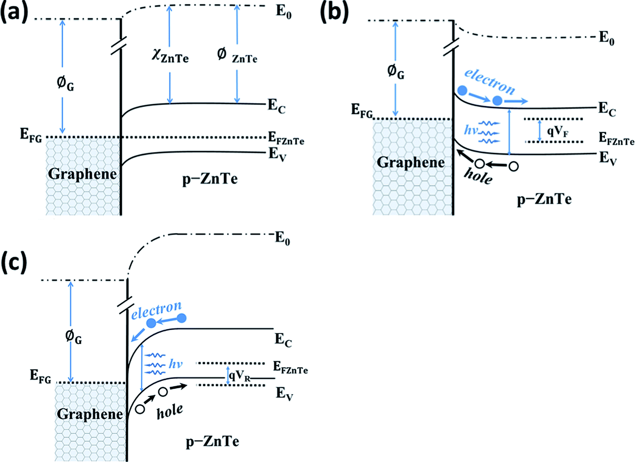 | ||
| Fig. 8 Energy band diagram of ZnTe NW/graphene Schottky diodes at (a) zero bias, (b) forward bias, (c) reverse bias. | ||
Conclusions
In summary, we present a synthetic method to prepare p-type ZnTe:Ga NWs by using a simple thermal evaporation method, in which Ga/Ga2O3 powder was used as the dopant. Electrical analysis reveals that the Ga doping led to p-type conduction characteristics, and the conductivity could be tuned over four orders of magnitude by varying the doping level. It is also found that when the Ga content in the ZnTe NWs increases from 1.3 to 5.1–8.7%, the hole mobility and hole concentration will increase from 0.0069, to 0.33 and 0.46 cm2 V−1 s−1 and from 2.4 × 10¹⁷, to 1.3 × 10¹⁸ and 5.6 × 1018 cm−3, respectively. Moreover, optoelectronic characterization of photodetector composed of ZnTe:Ga NW/graphene Schottky diodes shows that the device exhibits high sensitivity to light illumination with good reproducibility at both forward and revers bias voltages. It is believed that the as-doped p-type ZnTe:Ga NWs with tunable electrical properties will have potential application for fabricating new-generation nanoelectronic and nano-optoelectronic devices.Acknowledgements
This work was supported by the Natural Science Foundation of China (NSFC, nos 21101051, 61106010, 21205026, 21401036), the Natural Science Foundation of Anhui Province of China (no. 140808MB31) and the Fundamental Research Funds for the Central Universities (2012HGCX0003, 2013HGCH0012, 2014HGCH0005).References
- J. S. Jie, W. J. Zhang, I. Bello, C. S. Lee and S. T. Lee, Nano Today, 2010, 5, 313 CrossRef CAS PubMed.
- B. Nie, L. B. Luo, J. J. Chen, J. G. Hu, C. Y. Wu, L. Wang, Y. Q. Yu, Z. F. Zhu and J. S. Jie, Nanotechnolgy, 2013, 24, 095603 CrossRef PubMed.
- C. Xie, L. B. Luo, L. H. Zeng, L. Zhu, J. J. Chen, B. Nie, J. G. Hu, Q. Li, C. Y. Wu and J. S. Jie, CrystEngComm, 2012, 14, 7222 RSC.
- R. M. Ma, L. Dai, H. B. Huo, W. J. Xu and G. G. Qin, Nano Lett., 2007, 7, 3300 CrossRef CAS PubMed.
- B. Nie, J. G. Hu, L. B. Luo, C. Xie, L. H. Zeng, P. Lv, F. Z. Li, J. S. Jie, M. Feng, C. Y. Wu, Y. Q. Yu and S. H. Yu, Small, 2013, 9, 2872 CrossRef CAS PubMed.
- Y. Dai, B. Yu, Y. Ye, P. C. Wu, H. Meng, L. Dai and G. G. Qin, J. Mater. Chem., 2012, 22, 18442 RSC.
- F. Z. Li, L. B. Luo, Q. D. Yang, D. Wu, C. Xie, B. Xie, J. S. Jie, C. Y. Wu and S. H. Yu, Adv. Energy Mater., 2013, 3, 579 CrossRef CAS.
- C. Soci, A. Zhang, B. Xiang, S. A. Dayeh, D. P. R. Aplin, J. Park, X. Y. Bao, Y. H. Lo and D. Wang, Nano Lett., 2007, 7, 1003 CrossRef CAS PubMed.
- X. X. Wang, W. S. Zhang, G. L. Song, B. S. Zou, Z. S. Li, S. Guo, J. Li, Q. S. Li and R. B. Liu, RSC Adv., 2014, 4, 52550 RSC.
- L. B. Luo, X. L. Huang, M. Z. Wang, C. Xie, C. Y. Wu, J. G. Hu, L. Wang and J. A. Huang, Small, 2014, 13, 2645 CrossRef PubMed.
- M. C. Schlamp, X. G. Peng and A. P. Alivisatosa, J. Appl. Phys., 1997, 82, 5837 CrossRef CAS PubMed.
- J. I. Wong, N. Mishra, G. C. Xing, M. J. Li, S. Chakrabortty, T. C. Sum, Y. M. Shi, Y. T. Chan and H. Y. Yang, ACS Nano, 2014, 8, 2873 CrossRef CAS PubMed.
- S. Lee, H. Kim, D. J. Yun, S. W. Rhee and K. Yong, Appl. Phys. Lett., 2009, 95, 262113 CrossRef PubMed.
- C. Xie, B. Nie, L. Zhu, L. H. Zeng, Y. Q. Yu, X. H. Wang, Q. L. Fang, L. B. Luo and Y. C. Wu, Nanotechnology, 2013, 24, 355203 CrossRef PubMed.
- J. M. Wu and C. C. Kao, RSC Adv., 2014, 4, 13882 RSC.
- L. H. Zhang, L. L. Fan, Z. Li, E. Z. Shi, X. M. Li, H. B. Li, C. Y. Ji, Y. Jia, J. Q. Wei, K. L. Wang, H. W. Zhu, D. H. Zhu and A. Y. Cao, Nano Res., 2011, 4, 891 CrossRef CAS PubMed.
- A. Goudarzi, A. D. Namghi and C. S. Ha, RSC Adv., 2014, 4, 59764 RSC.
- A. Erlacher, M. Ambrico, G. Perna, L. Schiavulli, T. Ligonzo, H. Ligonzo and B. Ullrich, Appl. Surf. Sci., 2005, 248, 402 CrossRef CAS PubMed.
- Q. Zhang, J. Zhang, M. I. B. Utama, B. Peng, M. de la Mata, J. Arbiol and Q. H. Xiong, Phys. Rev. B: Condens. Matter Mater. Phys., 2012, 85, 085418 CrossRef.
- E. Groeneveld, S. V. Berkum, A. Meijerink and C. D. M. Donegá, Small, 2011, 7, 1247 CrossRef CAS PubMed.
- K. P. Acharya, A. Erlacher and B. Ullrich, Thin Solid Films, 2007, 515, 4066 CrossRef CAS PubMed.
- A. E. Rakhshani and S. Thomas, J. Mater. Sci., 2013, 48, 6386 CrossRef CAS.
- Q. Wu, M. Litz and X. C. Zhang, Appl. Phys. Lett., 1996, 68, 2924 CrossRef CAS PubMed.
- T. Tanaka, K. M. Yu, P. R. Stone, J. W. Beeman, O. D. Dubon, L. A. Reichertz, V. M. Kao, M. Nishio and W. Walukiewicz, J. Appl. Phys., 2010, 108, 024502 CrossRef PubMed.
- L. Li, Y. W. Yang, X. H. Huang, G. H. Li and L. D. Zhang, J. Phys. Chem. B, 2005, 109, 12394 CrossRef CAS PubMed.
- E. Janik, P. Dluzewski, S. Kret, A. Presz, H. Kirmse, W. Neumann, W. Zaleszczyk, L. T. Baczewski, A. Petroutchik, E. Dynowska, J. Sadowski, W. Caliebe, G. Caliebe and T. Wojtowicz, Nanotechnology, 2007, 18, 475606 CrossRef.
- D. Wu, Y. Jiang, Y. G. Zhang, Y. Q. Yu, Z. F. Zhu, X. Z. Lan, F. Z. Li, C. Y. Wu, L. Wang and L. B. Luo, J. Mater. Chem., 2012, 22, 23272 RSC.
- Z. Li, J. Salfi, C. D. Souza, P. Sun, S. V. Nair and H. E. Ruda, Appl. Phys. Lett., 2010, 97, 063510 CrossRef PubMed.
- L. Li, Y. W. Yang, X. H. Huang, G. H. Li and L. D. Zhang, J. Phys. Chem. B, 2005, 109, 12394 CrossRef CAS PubMed.
- S. Y. Li, Y. Jiang, D. Wu, L. Wang, H. H. Zhong, B. Wu, X. Z. Lan, Y. Q. Yu, Z. B. Wang and J. S. Jie, J. Phys. Chem. C, 2010, 114, 7980 CAS.
- H. B. Huo, L. Dai, C. Liu, L. P. You, W. Q. Yang, R. M. Ma, G. Z. Ran and G. G. Qin, Nanotechnology, 2006, 17, 5912 CrossRef CAS.
- M. Z. Wang, W. J. Xie, H. Hu, Y. Q. Yu, C. Y. Wu, L. Wang and L. B. Luo, Appl. Phys. Lett., 2013, 103, 213111 CrossRef PubMed.
- P. A. Hu, Z. Z. Wen, L. F. Wang, P. H. Tan and K. Xiao, ACS Nano, 2014, 6, 5988 CrossRef PubMed.
- B. Y. Zu, B. Lu, Y. N. Guo and X. C. Dou, J. Mater. Chem. C, 2014, 2, 2045 RSC.
- Y. Q. Yu, J. S. Jie, P. Jiang, L. Wang, C. Y. Wu, Q. Peng, X. W. Zhang, Z. Wang, C. Xie, D. Wu and Y. Jiang, J. Mater. Chem., 2011, 21, 12632 RSC.
- D. Wu, Y. Jiang, X. D. Yao, Y. J. Chang, Y. G. Zhang, Y. Q. Yu, Z. F. Zhu, Y. Zhang, X. Z. Lan and H. H. Zhong, J. Mater. Chem. C, 2014, 2, 6547 RSC.
| This journal is © The Royal Society of Chemistry 2015 |