Cubic to amorphous transformation of Se in silica with improved ultrafast optical nonlinearity
K. A. Ann Marya,
N. V. Unnikrishnan*a and
Reji Philipb
aSchool of Pure & Applied Physics, Mahatma Gandhi University, Kottayam-686560, India. E-mail: nvu100@yahoo.com
bLight and Matter Physics Group, Raman Research Institute, C. V. Raman Avenue, Sadashivanagar, Bangalore-560080, India
First published on 8th January 2015
Abstract
We report a cubic to amorphous transformation of selenium in silica xerogel prepared through a sol–gel route. The crystalline nature of the nanoparticles examined from the SAED pattern and HRTEM revealed an α-cubic structure. The band gap energies calculated from the UV-vis absorption measurements showed a higher band gap of 3.5 eV for the cubic form compared to 2.4 eV for the amorphous form. The ultrafast optical nonlinearity of the samples was investigated by an open aperture Z-scan at 800 nm using 100 fs laser pulses. Although doping with cubic Se did not improve the optical limiting efficiency of silica xerogels, doping with amorphous Se results in substantial enhancement. Numerical analysis of the Z-scan data attributed the nonlinearity to two-photon and three-photon absorption and two-photon induced free carrier absorption. These intensity-dependent, instantaneous nonlinearities make amorphous Se doped silica xerogels attractive candidates for the design of ultrafast optical limiter devices.
1. Introduction
Over the last two decades, there has been significant interest in the study of the different allotropic forms of materials and an exploration of their fundamental physics because of their potential applications in a wide range of fields, including photovoltaic devices, biomedical sensing and nonlinear optics. For example, the different crystalline allotropic phases of carbon have initiated intense research in recent years owing to their extraordinary electrical, thermal, optical, and mechanical properties, which promise a multitude of applications.1–5 Although graphite, diamond, fullerenes, carbon nanotubes, and graphene are generally poised as potential active components for nanosized devices, the fact that selenium allotropes also possess exceptional optical and electronic properties is sometimes overlooked. Selenium exists in different allotropic forms including an amorphous form6 consisting of a mixture of disordered chains and rings. The five crystalline states of Se include the monoclinic form, the most stable trigonal form, and the less reported cubic form. Among these, nanostructures of amorphous and trigonal forms of Se have been studied most widely because of the ease of growth and formation.7–12 The cubic form exists at normal pressures with unit cell constants, a = 2.970 Å and 5.755 Å for α and β cubic Se, respectively.6 Although the synthesis of cubic Se has not been explored well, β cubic Se nanoparticles have been synthesized through the biological reduction of SeO3 using the Pseudomonas aeruginosa strain, JS-11.13 Similarly, the biosynthesis of face-centered cubic (fcc) Se nanoparticles with DNA damaging properties has been carried out using lemon plant extract.14Selenium and its compounds have a remarkable position in technology because of their ability to form semiconducting QDs with fascinating applications in solar cells, xerography and imaging.15–17 They can be incorporated into glass via a sol–gel process, providing a simple fabrication route for the development of new classes of materials with potential optical and industrial applications. Moreover, selenium-based compounds are promising candidates for nonlinear optical applications in the ultrafast excitation domain. The optical nonlinearity of allotropes of selenium nanostructures – amorphous selenium nanoparticles and trigonal selenium nanowires – was studied recently on the femtosecond and nanosecond time scales.18 The incorporation of semiconductor nanocrystallites in strained glassy host matrices can help avoid degradation, and it also improves the stability for nonlinear optical applications, providing large optical nonlinearities and fast responses. Multiwalled carbon nanotubes (MWCNT) dispersed homogeneously in silica exhibited sustainable nonlinear optical properties for nanosecond excitation at 532 nm and 1064 nm laser wavelengths.19 Similarly, through the doping of Cu7.2S4 quantum dots, an enhancement in the third-order nonlinear optical properties of sodium borosilicate glass was measured using the Z-scan technique for femtosecond (ultrafast) excitation.20
Apart from the biological production of cubic Se by bacteria, to the best of our knowledge, there are no reports on the chemical synthesis and characterization of cubic Se nanocrystallites. Therefore, this paper reports the synthesis of cubic and amorphous Se nanoparticles through the sol–gel route. Their structural, crystalline and optical properties were examined in detail, and their nonlinear optical properties were studied using ultrafast (100 fs) laser pulses at 800 nm according to the open aperture Z-scan technique.
2. Experimental section
2.1. Synthesis of Se doped silica
Silica glasses with 10 wt% Se were prepared by the sol–gel process with tetraethyl orthosilicate (TEOS) as the precursor in the presence of ethanol and doubly distilled water. A measured volume of a 1 M HNO3 solution was added as a catalyst. The TEOS–H2O–HNO3 molar ratio was 1![[thin space (1/6-em)]](https://www.rsc.org/images/entities/char_2009.gif) :
:![[thin space (1/6-em)]](https://www.rsc.org/images/entities/char_2009.gif) 12
12![[thin space (1/6-em)]](https://www.rsc.org/images/entities/char_2009.gif) :
:![[thin space (1/6-em)]](https://www.rsc.org/images/entities/char_2009.gif) 0.01. Se nanocrystallites were prepared by the decomposition reaction of selenous acid, and were incorporated into the SiO2 matrix by annealing. An appropriate amount of selenous acid dissolved in doubly distilled water and ethanol was poured into TEOS and stirred at room temperature. The resulting mixture was stirred continuously for approximately one hour at room temperature until it formed a clear solution. The mixture (sol) was poured into polypropylene containers, which were then sealed and kept for one month to form a stiff gel.
0.01. Se nanocrystallites were prepared by the decomposition reaction of selenous acid, and were incorporated into the SiO2 matrix by annealing. An appropriate amount of selenous acid dissolved in doubly distilled water and ethanol was poured into TEOS and stirred at room temperature. The resulting mixture was stirred continuously for approximately one hour at room temperature until it formed a clear solution. The mixture (sol) was poured into polypropylene containers, which were then sealed and kept for one month to form a stiff gel.
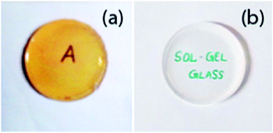
The samples were then heated in a hot air oven at 60 °C for three days to eliminate the organics and water present. Finally, the samples were annealed at 200 °C at a heating rate of 30 °C h−1 in a programmable furnace for two hours. The color of the xerogel turned to deep orange upon heating. The compositions of the prepared samples are summarized in Table 1. A photograph of the Se doped sample is shown in Fig. 1.
| Sample name | Wt% Se | Temperature |
|---|---|---|
| a-Se | 10% | 200 °C |
| c-Se | 10% | 60 °C |
2.2. Optical and morphological characterizations
The morphological and crystalline nature of the nanoparticles were examined by transmission electron microscopy (TEM) and SAED using a JEM 2100 electron microscope. Elemental analysis was performed by energy dispersive X-ray (EDX) spectroscopy obtained from a scanning electron microscope (SEM, JEOL JSM 6390). FTIR spectroscopy of the samples in the region 400–4000 cm−1 was conducted using a Shimadzu FTIR spectrometer 8400 S for structural analysis. The UV-visible absorption spectra and emission spectra of the samples were measured using a spectrophotometer (Shimadzu-UVPC2401) and spectrofluorophotometer (Fluoromax-4-Horiba Jobin Yvon), respectively.2.3. Nonlinear optical experiments
The intensity-dependent nonlinear optical transmission of pure silica and c-Se and a-Se doped silica were measured using the open aperture Z-scan21 technique. A regeneratively amplified Ti:sapphire laser emitting 100 fs laser pulses at 800 nm was used as the excitation source. Neutral density filters were used to set the laser pulse energy to the required values. The laser beam was focused using a converging lens so that the maximum intensity was experienced at the beam focus. Although the laser was run at a repetition rate of 10 Hz, the experiment was effectively done in single-shot mode by employing a fast mechanical shutter in the beam path. The samples loaded on a programmable linear translation stage were scanned along the beam axis through the beam focus. The sample experiences a different laser intensity at each position, and its transmission varies as a function of the intensity due to the nonlinearity. The transmitted energy for each position was measured using a pyroelectric detector. The experiment was automated using a LabVIEW program.3. Results and discussion
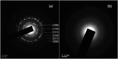
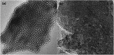
The crystalline structure and morphology of the 10 wt% Se doped silica was examined from the SAED patterns (Fig. 2) and TEM (Fig. 3 and 4). For a-Se, the SAED pattern clearly shows the amorphous nature of the sample. The prominent rings in the SAED pattern of c-Se can be indexed to a pure cubic structure (ICDD no. 38-0768). The d-spacings obtained at 3.065 Å, 1.942 Å, 1.669 Å, 1.3513 Å, 1.235 Å, and 1.043 Å were assigned to the (100), (110), (111), (210), (211), and (300) lattice planes of the cubic phase of Se, respectively. The formation of uniform nanoparticles ranging in size from 3 to 6 nm and 4 to 8 nm (for cubic and amorphous Se respectively) can be observed from the TEM images (Fig. 3(a) and 4(b)).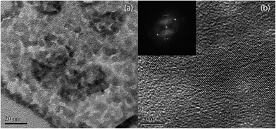 | ||
| Fig. 4 TEM (a) and HRTEM (b) of cubic Se doped silica. The FFT pattern of the lattice planes in HRTEM is shown in the inset. | ||
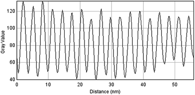
Fig. 3(b) shows the HRTEM image of amorphous Se doped silica, which does not contain any fringe spacings, confirming the formation of an amorphous phase. HRTEM of cubic Se (Fig. 4(b)) revealed high crystallinity with well resolved lattice fringes throughout the whole particle with a d-spacing of 3.016 Å, which can be assigned to the (100) plane of cubic Se. Correspondingly, the fast Fourier transform (FFT) of the image shown in Fig. 4 is in excellent agreement with the calculated diffraction pattern of the cubic Se structure, which was aligned along the (100) plane of cubic Se with a d-spacing of 2.991 Å. A more detailed analysis of the inter-planar spacing was conducted from image processing applied to the magnified image by surface plot analysis generated from ImageJ software. The surface plot obtained by selecting a square area of parallel lattice fringes in the magnified image is shown in Fig. 5. The interplanar distance of the (100) plane obtained from the ratio of distance and the number of peaks was compared with those obtained from the HRTEM and SAED pattern (Table 2).
| dSAED (Å) | dHRTEM (Å) | dFFT (Å) | dsurface plot (Å) |
|---|---|---|---|
| 3.065 | 3.016 | 2.991 | 3.034 |
The formation of cubic Se in silica can be explained as follows. Se exists in a number of allotropic phases, among which the stable trigonal phase has been studied widely. As trigonal Se has a highly anisotropic structure, the growth direction is largely confined to a preferred direction (c-axis).11,22 In our experiment, the silica matrix was crossly interlinked due to the network chains, and Se remained occupied in the nanopores of mesoporous silica. Their growth in a preferred orientation was inhibited due to the capping effect and an isotropic cubic structure was maintained. In such a mesoporous matrix, Se nanoparticles show uniform growth in all directions. Therefore, these particles can crystallize into a structure more symmetrical than the trigonal structure. The aforesaid mechanism leads to the formation of cubic selenium in the pores of the silica matrix.
In general, a crystalline to an amorphous phase transformation rarely occurs. However, heat treatment near the melting point of a crystal would fuse the crystals to an amorphous form. For Se, the melting temperature of different forms lies in the range, 100–200 °C.6 Hence, heat treatment at 200 °C would melt cubic Se, resulting in the formation of an amorphous phase. This type of phase transformation may lead to the agglomeration of nanoparticles, which is evident from the TEM image of a-Se NPs. The amorphous form of Se is less stable but a stable form of Se NPs is obtained by effectively capping the NPs. The silica matrix can hold a-Se NPs within the nanopores in a stable form.
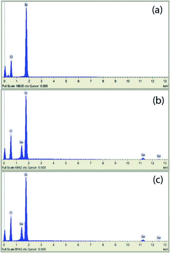
EDX spectroscopy was used to further identify the chemical composition of the particles, which clearly indicated that the Se doped silica sample is composed of Si, O and Se, as expected. Both c-Se and a-Se give similar EDS spectra, and the spectrum of pure silica is given as a reference (Fig. 6).
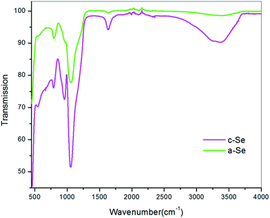
The FTIR spectra of 10 wt% Se doped silica glass dried at 60 °C and 200 °C are shown in Fig. 7. The spectra of the Se nanoparticle-embedded silica glass were similar to the spectrum of pure SiO2 (ref. 23) with strong bands associated with Si–O stretching and bending vibrations. These bands were observed at 799 and 1057 cm−1. The broad absorption around 3325 cm−1 indicates the presence of water (hydroxyl group). For a-Se doped silica, the bands due to the presence of absorbed water decrease in intensity with increasing annealing temperature. Moreover, weak absorption at 1645 and 965 cm−1 indicates the presence of an oxyethyl group, which decreases with heat treatment. This indicates the gradual strengthening of the silica network through cross-linking.
The optical excitation of electrons across the band gap is strongly permitted, producing an abrupt increase in absorption at the wavelength corresponding to the gap energy. This feature in the optical spectrum is known as the absorption edge. The absorption spectra of Se doped silica glass dried at 60 °C and 200 °C are shown in Fig. 8. The direct absorption band gap of semiconductor nanoparticles can be determined from the equation,
| αhν = B(hν − Eg)1/2, | (1) |
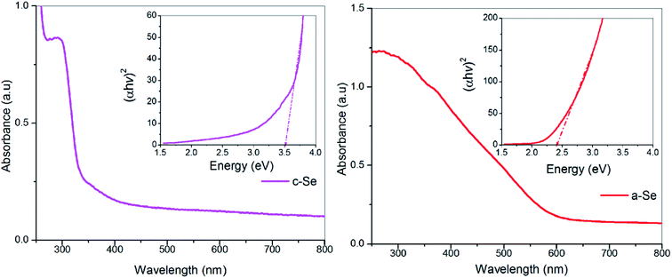 | ||
| Fig. 8 Absorption spectra of c-Se and a-Se doped silica. The Tauc plots given in the insets give bandgaps of 3.5 eV and 2.4 eV, respectively. | ||
The calculated band gap for a-Se doped silica is comparable to that of the reported values.18 In addition, the band gap energy was blue-shifted relative to the bulk band gap due to the quantum size effect. On the other hand, the band structures of cubic Se have not been investigated in detail. The observed absorption spectrum is similar to that obtained for fcc Se nanoparticles with an absorption maximum at 395 nm.14 As the trigonal structure of Se is closely related to the simple cubic structure, with just a small trigonal distortion, the band to band transitions in cubic form can be approximated to that of a trigonal structure.24 For trigonal Se, the first excitonic peak is associated with direct transitions at 1.95 eV and the second excitonic peak is associated with a band edge transition at 3.09 eV.25 Hence, the observed band gap of 3.5 eV for cubic Se due to exciton absorption can be considered to be blue shifted due to quantum confinement.
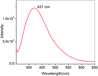
The photoluminescence spectrum of c-Se doped silica measured at an excitation wavelength of 340 nm is shown in Fig. 9. For a-Se doped silica, no emission was observed, which is in agreement with earlier reports.18 For trigonal Se nanowires, excitation at 266 nm and 350 nm resulted in PL emission peaking at 335 and 429 nm, respectively.18 Reports of PL from the cubic form are rare because only the amorphous and trigonal forms of selenium are usually studied in detail. Moreover, calculations of the band structure, density of states and charge densities of the cubic form of Se are uncommon. Therefore, the optical transition behind the observed emission band could not be fully explained. As the band gap obtained for c-Se is 3.5 eV, the emission band observed at an excitation of 3.6 eV is the band edge emission. Similar band edge emission was observed in fcc selenium nanoparticles synthesized using a leaf extract, where an emission peak was observed at 525 nm from 395 nm excitation.14
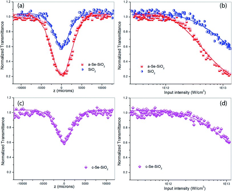
The changes in the absorptivity of a material induced by a strong beam of light can be measured using the open aperture Z-scan technique. The intensity dependent nonlinear transmissions measured for ultrafast excitation are shown in Fig. 10. The samples used have a linear transmittance of 85% at an excitation wavelength of 800 nm. The open aperture Z-scan curves exhibit valleys indicating reverse saturable absorption with a-Se doped silica exhibiting the deepest valley. For c-Se doped silica the Z-scan curve has a depth similar to that of pure silica. The nonlinear transmission as a function of the input intensity is plotted in Fig. 10(b and d). From these curves, it is obvious that the optical limiting efficiency is enhanced for a-Se doped silica matrix.
To understand the mechanism behind this intensity-dependent instantaneous absorptive nonlinearity, the experimental Z-scan curves were fitted numerically to the relevant nonlinear transmission equations. For the pure silica matrix and c-Se doped silica, the obtained nonlinear transmission data was found to fit well to a model, in which SA occurs along with 2PA and ESA. The nonlinear absorption coefficient is given by the general expression,
 | (2) |
 | (3) |
The best fit for nonlinear absorption in a-Se silica was obtained using a model that includes 3PA/ESA in addition to 2PA/ESA and saturable absorption. The corresponding propagation equation is given by
 | (4) |
| Material | Is (W m−2) | βeff (m W−1) | γeff (m3 W−2) |
|---|---|---|---|
| SiO2 | 5.5 × 10¹⁵ | 4.8 × 10⁻¹⁵ | — |
| c-Se–SiO2 | 5.4 × 10¹⁵ | 4.8 × 10⁻¹⁵ | — |
| a-Se–SiO2 | 5.4 × 10¹⁵ | 4.9 × 10⁻¹⁵ | 3.4 × 10⁻³¹ |
For ultrafast excitation at 10 μJ energy, the silica matrix itself exhibits weak nonlinearity through the combined effects of saturable absorption and two photon absorption (2PA). The observed nonlinear absorption in amorphous silica can be attributed to point defects generated from the imperfect SiO4 continuous network. The defects include oxygen vacancies (5 eV) and oxygen surplus (3.8 eV), nonbridging oxygen hole centers (1.9 eV), two-fold coordinated silicon lone pair centers (3.1 eV), etc.28–30 Oxygen-deficient high-purity silica glasses (2.7 eV) have also been studied by luminescence lifetime measurements.31
The difference in the optical limiting efficiency of c-Se doped silica and a-Se doped silica arises from the influence of the crystal form on nonlinear absorption. The electronic structure and density of states differ as we go from one crystalline form to another. This in turn results in different optical absorption spectra for c-Se and a-Se doped silica. As observed from the UV-vis absorption spectra, the optical band gap of the cubic and amorphous forms are 3.5 eV and 2.4 eV respectively. For the cubic form, the condition, 2hν ≥ Eg, is not satisfied and hence two-photon absorption occurring across the band gap is weak. Therefore, c-Se cannot modify the optical limiting efficiency of silica. On the other hand, for a-Se doped silica, the condition, 2hν ≥ Eg, is satisfied, and excitation at 1.55 eV can lead to the simultaneous absorption of two photons to higher energy levels in the conduction band followed by free carrier absorption from the conduction band. For example, nonlinear optical absorption in Zn(1−x)MgxO thin films excited by ultrafast pulses at 800 nm has been reported to arise from two-photon induced free carrier absorption.32 In addition to the genuine two-photon and two-photon induced free carrier absorption, the nonlinearity may also have contributions from genuine three-photon absorption. The enhanced ultrafast nonlinearity measured in a-Se doped silica indicates the potential for developing optical limiter glasses that can protect sensitive optical sensors from laser-induced damage.
4. Conclusion
Silica xerogels doped with cubic and amorphous Se were prepared through a sol–gel route. The structural properties of the silica xerogels were investigated in detail by FTIR spectroscopy. The optical properties of the cubic and amorphous phases of selenium nanoparticles were studied from UV-vis absorption measurements over the entire visible spectral range, and from the photoluminescence spectra. The mean size of the nanoparticles was estimated from the TEM images while the crystalline nature was examined by SAED. The crystalline cubic structure was confirmed by HRTEM, which clearly showed lattice fringes with randomly oriented nanocrystallites. The ultrafast optical nonlinearity of amorphous Se doped xerogel glasses investigated by the open aperture Z-scan technique revealed enhanced nonlinear absorption at 800 nm. No such enhancement was observed for cubic Se doped glasses. The optical nonlinearity was dominated by nonlinear absorption resulting from two-photon and three-photon absorption and two-photon induced excited state absorption. These intensity-dependent, instantaneous nonlinearities with a fast response make amorphous Se doped xerogel glasses attractive candidates for ultrafast optical limiter applications.Acknowledgements
KAAM gratefully acknowledges Kerala State Council for Science Technology and Environment for the award of a Research Fellowship. RP wishes to thank DST, Government of India, for grants through the Australia-India Strategic Research Fund (AISRF) program.References
- J. D. Fidelus, E. Wiesel, F. H. Gojny, K. Schulte and H. D. Wagner, Composites, Part A, 2005, 36, 1555 CrossRef PubMed.
- X. Zhao, Q. Zhang, D. Chen and P. Lu, Macromolecules, 2010, 43, 2357 CrossRef CAS.
- G. Eda and M. Chhowalla, Nano Lett., 2009, 9, 814 CrossRef CAS PubMed.
- A. Ltaief, A. Bouazizi, J. Davenas, R. Ben Chaâbane and H. Ben Ouada, Synth. Met., 2004, 147, 261 CrossRef CAS PubMed.
- A. F. Hebard, R. C. Haddon, R. M. Fleming and A. R. Kortan, Appl. Phys. Lett., 1991, 59, 2109 CrossRef CAS PubMed.
- V. S. Minaev, S. P. Timoshenkova and V. V. Kalugina, J. Optoelectron. Adv. Mater., 2005, 7, 1717 CAS.
- L. Liu, Q. Peng and Y. Li, Nano Res., 2008, 1, 403 CrossRef CAS.
- Z. Liao, C. Hou, L. Liu and D. Yu, Nanoscale Res. Lett., 2010, 5, 926 CrossRef CAS PubMed.
- Y. Chen, W. Zhang, F. Zhanb, Z. Zhang, B. Zhou and H. Li, Mater. Lett., 2004, 58, 2761 CrossRef CAS PubMed.
- Q. Li and V. W. Yam, Chem. Commun., 2006, 1006 RSC.
- B. Gates, B. Mayers, B. Cattle and Y. Xia, Adv. Funct. Mater., 2002, 12, 219 CrossRef CAS.
- J. Song, J. Zhu and S. Yu, J. Phys. Chem. B, 2006, 110, 23790 CrossRef CAS PubMed.
- S. Dwivedi, A. A. AlKhedhairy, M. Ahamed and J. Musarrat, PLoS One, 2013, 8, e57404 CAS.
- K. S. Prasad, H. Patel, T. Patel, K. Patel and K. Selvaraj, Colloids Surf., B, 2013, 103, 261 CrossRef CAS PubMed.
- I. Robel, V. Subramanian, M. Kuno and P. V. Kamat, J. Am. Chem. Soc., 2006, 128, 2385 CrossRef CAS PubMed.
- N. Pradhan, D. M. Battaglia, Y. Liu and X. Peng, Nano Lett., 2007, 7, 312 CrossRef CAS PubMed.
- C. X. Yin, T. Yang, W. Zhang, X. D. Zhou and K. Jiao, Chin. Chem. Lett., 2010, 21, 716 CrossRef CAS PubMed.
- K. A. Ann Mary, N. V. Unnikrishnan and R. Philip, Chem. Phys. Lett., 2013, 588, 136 CrossRef CAS PubMed.
- C. Zheng, M. Feng, Y. Du and H. Zhan, Carbon, 2009, 47, 2889 CrossRef CAS PubMed.
- W. Xiang, H. Zhao, J. Zhong, Y. Guo, Z. Chen, H. Luo, X. Zhao, X. Liang and X. Yang, J. Non-Cryst. Solids, 2012, 358, 2641 CrossRef CAS PubMed.
- M. Sheik Bahae, A. A. Said, T. M. Wei, D. J. Hagan and E. W. Van Stryland, IEEE J. Quantum Electron., 1990, 26, 760 CrossRef CAS.
- X. Li, Y. Li, S. Li, W. Zhou, H. Chu, W. Chen, I. L. Li and Z. Tan, Cryst. Growth Des., 2005, 5, 911 CAS.
- M. Epifani, G. De, A. Licciulli and L. Vasanelli, J. Mater. Chem., 2001, 11, 3326 RSC.
- J. D. Joannopoulos, M. Schluter and M. L. Cohen, Phys. Rev. B: Solid State, 1975, 11, 2186 CrossRef CAS.
- S. Tutihasi and I. Chen, Phys. Rev., 1967, 158, 623 CrossRef CAS.
- P. Chen, X. Wu, X. Sun, J. Lin, W. Ji and K. L. Tan, Phys. Rev. Lett., 1999, 82, 2548 CrossRef CAS.
- J. Wang, Y. Hernandez, M. Lotya, J. N. Coleman and W. J. Blau, Adv. Mater., 2009, 21, 2430 CrossRef CAS.
- H. Nishikawa, R. Tohmon, Y. Ohki, K. Nagasawa and Y. Hama, J. Appl. Phys., 1989, 65, 4672 CrossRef CAS PubMed.
- I. A. Rahman and V. Padavettan, J. Nanomater., 2012, 2012, 8 Search PubMed.
- Y. Sakurai, J. Non-Cryst. Solids, 2000, 271, 218 CrossRef CAS.
- R. Tohmon, Y. Shimogaichi, H. Mizuno, Y. Ohki, K. Nagasawa and Y. Hama, Phys. Rev. Lett., 1989, 62, 1388 CrossRef CAS.
- C. S. Suchand Sandeep, R. Philip, R. Satheeshkumar and V. Kumar, Appl. Phys. Lett., 2006, 89, 063102 CrossRef PubMed.
| This journal is © The Royal Society of Chemistry 2015 |

