Subramani Thiyagua,
Hong-Jhang Syua,
Chen-Chih Hsueha,
Chien-Ting Liua,
Tzu-Ching Linb and
Ching-Fuh Lin*abc
aGraduate Institute of Photonics and Optoelectronics, National Taiwan University, Taipei 10617, Taiwan, Republic of China. E-mail: lincf@ntu.edu.tw
bGraduate Institute of Electronics Engineering, National Taiwan University, Taipei 10617, Taiwan, Republic of China
cDepartment of Electrical Engineering, National Taiwan University, Taipei 10617, Taiwan, Republic of China
First published on 16th January 2015
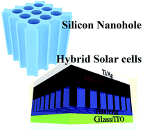
In this paper, we employ a series of metal-assisted chemical etching processes to fabricate low-cost silicon nanohole (SiNH) and silicon nanowire (SiNW) arrays for hybrid solar cells. The SiNH arrays and SiNW arrays are obtained by a two-step etching and one-step etching technique, respectively. Length and depth of SiNWs and SiNHs can be controlled by etching time. The SiNH arrays demonstrate higher optical trapping effect than SiNW arrays, resulting in leading performance power conversion efficiency of 11.25% in the hybrid organic–inorganic solar cells. SiNH arrays have a high surface area, compared to SiNW arrays, so they can give rise to more junction area in the organic–inorganic heterojunction structures. In addition, these SiNH arrays possess additional advantages of robust structures and higher density with low air-filling fraction as compared to SiNW arrays. Furthermore, the SiNH arrays show superior efficiency to SiNW arrays experimentally. In particular, the fabricated SiNH arrays with high density can suppress the optical reflection well below 5% over a broad wavelength range from 300 to 1100 nm in a short nanohole depth. The very low reflectance and excellent light trapping property are attributed to the sub-wavelength dimension of the SiNH structure. These SiNH arrays not only facilitate the optical trapping, but also provide efficient broadband and omnidirectional photon harvests for cost-effective future nanostructured photovoltaics.
On the other hand, intended for silicon nanohole (SiNH) arrays, G. Chen and X. Hu also obtained low reflectance and high absorptance through calculation.18,19 Theoretically, those results showed that SiNH arrays have weaker reflectance and stronger absorptance than silicon nanowire (SiNW) arrays in the Si absorption spectrum.18–20 In addition, SiNHs are found to exhibit higher efficiency and superior mechanical stability than SiNWs, appearing to be an alternative structure with great potential for photovoltaics.5,21,22 However, few literatures report the experimental optical properties of SiNH arrays and their applications in inorganic–organic hybrid solar cells.23 Therefore, in this paper, we report experimental investigation on the light trapping characteristics of silicon nanohole arrays in the solar spectrum and compare the results to those of silicon nanowire arrays. We find that light absorption of nanohole arrays is better than nanowire arrays. Also we calculate the air-filling fraction of SiNH arrays and SiNW arrays. It shows that SiNH arrays have high surface area so that it forms more junction area.
Regarding the solar-cell application, some SiNH and SiNW arrays were set up to cooperate with an organic conducting material poly(3,4-ethylenedioxythiophene):poly(styrenesulfonate) (PEDOT:PSS), to form heterojunction hybrid solar cells. Because the lowest unoccupied molecular orbital (LUMO) of PEDOT:PSS (−3.5 eV) is higher than the conduction band of Si, the electron transportation direction can be regulated toward cathode.8,9,15 Moreover, the highest occupied molecular orbital (HOMO) of PEDOT:PSS (−5.1 eV) is near the valence band of Si, so holes can transport from Si to PEDOT:PSS.
In this study, SiNH and SiNW arrays were fabricated by using two kinds of metal-assisted wet chemical etching (MacEtch) through solution processes. The fabricated Si-nanostructure length can be controlled by altering the etching time. The results reveal that SiNH arrays can produce a high density and low air-filling fraction. Optical characteristics of the as-generated SiNH and SiNW arrays were studied by measuring total reflectance using an integrated sphere over a wavelength range of 300–1100 nm. A comparison was made to the SiNH and SiNW arrays for studying optical trapping induced by silicon nanostructures. SiNH arrays have very low reflectance and higher optical trapping as compared to SiNW arrays. The very low reflectance and excellent light trapping property are attributed to the sub-wavelength dimension of the SiNH structure. The air-filling fraction for SiNWs increases when the etching time increases due to the aggregation of the nanowires. On the other hand, for SiNHs, the air-filling fraction is maintained at almost the same level because the etching gap is fixed and mainly determined at the step of Ag deposition. We also compared the SiNH/PEDOT:PSS hybrid solar cells to the SiNW/PEDOT:PSS device. SiNH hybrid solar cells with 170 nm depth have the leading performance. The highest short-circuit current density (Jsc) is 35.36 mA cm−2; open-circuit voltage (Voc) is 0.51 V; the fill factor (FF) is 62.36%; and the power conversion efficiency (PCE) is 11.25%.
![]() | ||
Fig. 1 Schematic diagram of etching techniques to fabricate silicon nanowire and silicon nanohole (a) SiNW formation – one step etching (b) and (c) SiNH formation – two step etching. |
![]() | ||
Fig. 2 Schematic representation of (a) silicon nanowire (b) silicon nanohole (c) silicon nanohole hybrid solar cell structure. |
For JV characteristic measurement, the device was illuminated from ITO side under 1 sun AM 1.5G 100 mW cm−2 by solar simulator SUN 2000, Abet Technologies, Inc, and measured by Keithley 2400 source meter. Scanning Electron Microscopic (SEM) pictures of Si nanohole were observed by LEO 1530 FE-SEM. The optical reflectance of Si nanohole was measured by JASCO V-670 UV-VIS spectrophotometer with the integrating sphere.
The SEM images of fabricated SiNH arrays are shown in Fig. 4. High-density nanoholes are homogenously distributed on Si wafer with an average silicon nanohole diameter size of 25 nm. The nanoholes are directly fabricated from electro-less metal deposition in HF/AgNO3 solution and then vertically etched in HF/H2O2 solution. During the process of electro-less metal deposition, Ag nano-particles are self-assembled via local reduction and oxidation between Ag+ and Si; therefore, the photolithography or template assisted is not needed.5,21 Usually, the two-step etching method is used to fabricate nanowires. In our method, we deposit tiny independent Ag nano-particles on the silicon wafer by controlling the deposition times, and the depth of the SiNH structure can then be controlled by the MacEtch etching time. Fig. 4(a)–(f) show the 45° tilted view of SiNH arrays with the etching time of 2, 7, 10, 17, 25, and 35 s. The corresponding depth of the nanohole is 50 nm, 130 nm, 170 nm, 290 nm, 470 nm, and 570 nm, respectively. As the etching time increases, the depth of the nanohole also increases.
To form the same depth of a silicon nanowire and nanohole, SiNH requires less etching time than SiNW, as shown in Table 1. Fig. 5(a)–(c) show the top-view SEM images of SiNW arrays with etching time of 1 min 2 s, 2 min 11 s, and 3 min 53 s. The corresponding length was shown in Table 1. Fig. 5(d)–(f) show the top-view SEM images of SiNH arrays with the etching time of 7 s, 17 s, and 35 s. The SiNW and SiNH top-view SEM images shown here have the same lengths. Before the SiNW and SiNH array morphology being investigated, according to the top-view SEM images, the density and air-filling fraction are calculated to express the morphology difference. For SiNW arrays, the wire density of 51 nm, 130 nm, 170 nm, 295 nm, 468 nm, 565 nm, and 710 nm SiNW arrays are 3.49 ± 0.08 × 10¹⁰, 3.39 ± 0.12 × 10¹⁰, 3.35 ± 0.06 × 10¹⁰, 3.22 ± 0.09 × 10¹⁰, 3.02 ± 0.11 × 10¹⁰, 2.88 ± 0.05 × 10¹⁰, and 2.17 ± 0.07 × 1010 cm−2, respectively. For SiNH arrays, the nanohole density of 50 nm, 130 nm, 170 nm, 290 nm, 470 nm, 570 nm, and 720 nm SiNH arrays are 1.90 ± 0.06 × 10¹¹, 1.60 ± 0.13 × 10¹¹, 1.51 ± 0.09 × 10¹¹, 1.29 ± 0.06 × 10¹¹, 1.05 ± 0.05 × 10¹¹, 1.04 ± 0.04 × 10¹¹, and 1.01 ± 0.02 × 1011 cm−2, respectively. The air-filling fraction refers to the silicon top surface area over total area. The air-filling fraction of SiNW arrays is 0.572 ± 0.002% for a SiNW length and time of 51 nm and 23 s, 0.649 ± 0.004% for a SiNW length and time of 130 nm and 1 min 2 s, 0.674 ± 0.008% for a SiNW length and time of 170 nm and 1 min 20 s, 0.681 ± 0.012% for a SiNW length and time of 295 nm and 2 min 11 s, 0.730 ± 0.009% for a SiNW length and time of 468 nm and 3 min 19 s, 0.765 ± 0.015% for a SiNW length and time of 565 nm and 3 min 53 s, and 0.791 ± 0.021% for a SiNW length and time of 710 nm and 4 min 41 s, respectively. Also, the air-filling fraction of SiNH arrays is 0.361 ± 0.022% for a SiNH length and time of 50 nm and 2 s, 0.434 ± 0.012% for a SiNH length and time of 130 nm and 7 s, 0.390 ± 0.011% for a SiNH length and time of 170 nm and 10 s, 0.410 ± 0.006% for a SiNH length and time of 290 nm and 17 s, 0.392 ± 0.009% for a SiNH length and time of 470 nm and 25 s, 0.407 ± 0.010% for a SiNH length and time of 570 nm and 35 s, and 0.396 ± 0.009% for a SiNH length and time of 720 nm and 50 s, respectively. All the parameters are listed in Table 1.
SiNW | SiNH | ||||||
---|---|---|---|---|---|---|---|
Etching condition (time) | Length (nm) | Density (×1010 cm−2) | Air filling fraction (%) | Etching condition (time) | Length (nm) | Density (×1011 cm−2) | Air filling fraction (%) |
23 s | 51 ± 2 | 3.49 ± 0.08 | 0.572 ± 0.002 | 2 s | 50 ± 2 | 1.90 ± 0.06 | 0.361 ± 0.022 |
1 min 2 s | 130 ± 2 | 3.39 ± 0.12 | 0.649 ± 0.004 | 7 s | 130 ± 3 | 1.60 ± 0.13 | 0.434 ± 0.012 |
1 min 20 s | 170 ± 1 | 3.35 ± 0.06 | 0.674 ± 0.008 | 10 s | 170 ± 2 | 1.51 ± 0.09 | 0.390 ± 0.011 |
2 min 11 s | 295 ± 5 | 3.22 ± 0.09 | 0.681 ± 0.012 | 17 s | 290 ± 3 | 1.29 ± 0.06 | 0.410 ± 0.006 |
3 min 19 s | 468 ± 4 | 3.02 ± 0.11 | 0.730 ± 0.009 | 25 s | 470 ± 4 | 1.05 ± 0.05 | 0.392 ± 0.009 |
3 min 53 s | 565 ± 5 | 2.88 ± 0.05 | 0.765 ± 0.015 | 35 s | 570 ± 2 | 1.04 ± 0.04 | 0.407 ± 0.010 |
4 min 41 s | 710 ± 10 | 2.17 ± 0.07 | 0.791 ± 0.021 | 50 s | 720 ± 5 | 1.01 ± 0.02 | 0.396 ± 0.009 |
![]() | ||
Fig. 5 Topview of SEM images of SiNW and SiNH arrays with the etching times of (a)–(c) 1 min 2 s, 2 min 11 s, and 3 min 53 s SiNW arrays, and (d)–(f) 7 s, 17 s, and 35 s SiNH arrays. |
According to the data listed in Table 1, SiNHs have high density as compared to the SiNW structure caused by the different etching mechanism of the SiNW and SiNH methods. For the SiNH method, Ag nanoparticles are independently distributed over the silicon wafer before etching. For the SiNW method, Ag deposition and HF etching occur concurrently and continuously. The etching gap is enlarged while the etching time increases. However, for the SiNH method, the etching gap is determined in the step of Ag deposition. Thus, the SiNHs have higher density than SiNWs. Also, SiNWs have the problem of aggregation, but SiNHs do not.
The SiNH etching method has a higher etching rate than the SiNW etching method. The SiNH etching rate is ∼15 nm s−1, but for SiNWs, the etching rate is ∼3 nm s−1. If silicon can be oxidized by an oxidant, like H2O2, HF can etch the Si quickly. This explicitly shows that a high concentration of HF and oxidant can form a nanostructure in a short time. Here, the silicon nanohole method has HF (6.57 mol L−1) and H2O2 (0.18 mol L−1), but SiNW method has 0.023 M Ag+ and 5.6 M HF. Therefore, SiNH method has a higher etching rate. In particular, the top morphology of nanoholes will change according to the etching time. In etching time of 2 to 10 s, the surface of the nanoholes has a uniform structure. However, when etching time is increased, slightly larger holes are formed (Fig. 4(c)–(f)), and rough surface is seen on top of the nanohole structure. In our experiment, we control the etching time to be less than 1 min for later applications. On the other hand, in the SiNW etching technique, more and more Ag was deposited and covered the top of SiNW arrays to form a thick layer as the etching time increased. From this evaluation and data listed in Table 1, we get the air-filling fraction plotted graph, as shown in Fig. 6. The air-filling fraction for SiNWs increases when the etching time increases due to aggregation of the nanowires; however, for SiNHs, the air-filling fraction is maintained at almost the same level because the etching gap is determined by the step of Ag deposition. From Fig. 6, we can clearly see that SiNHs have a low air-filling fraction, compared to SiNWs. This data deduce, from top-view SEM, images of both Si nanostructures. SiNHs have a higher surface area than SiNWs; a schematic representation is shown in Fig. S1.†
Silicon nanostructures can achieve low reflectance and high absorption because of effective light trapping, thereby increasing the average light path. One of the main purposes of Si nanostructures is to replace the conventional texture and anti-reflection coating. Optical reflectance of SiNWs and SiNHs with different depths is measured by integrated sphere from the range of visible to near-infrared region (300 nm–1100 nm), as shown in Fig. 7 for the comparison of optical reflectance between the referenced polished Si, SiNWs and SiNHs. We can clearly observe a significant suppression of optical reflectance in all wavelengths for both nanostructures as compared to polished silicon wafer. The etching time of SiNWs and SiNHs for an average depth of 50 nm is 23 s and 2 s, respectively. We can see that the SiNH structure has low reflectance as compared to the SiNW structure at the same depth level. SiNHs have a better light trapping effect due to high density and low air-filling fraction. Optical trapping between SiNWs and SiNHs will be discussed later. Fig. 7(b) shows the comparison of optical reflectance between the referenced polished Si. For SiNWs and SiNHs to reach an average depth of 130 nm, the etching time is 1 min 2 s and 7 s, respectively. Compared to SiNWs, SiNHs have a lower reflectance due to excellent light trapping effect.
The reflectance decreases while the nanowire and nanohole length increases for both of the etching methods in each wavelength. The distinctive characteristic of silicon nanohole is that they have minimum reflectance (Rmin) at a specific wavelength (λmin). The λmin will shift according to different porosity and thickness of the porous structure.24 The Rmin of SiNH, with the shallow depth of 170 nm, is as low as 1.6% at 515 nm (λmin). As the depth of the nanohole increases, the average reflectance decreases. The nanohole average reflectance of 470 nm depth is decreased to 3.8%. However, for SiNWs with the same length of 470 nm, the average reflectance is 7.5%. The total reflectance of longer nanowires or a deeper nanohole has low reflectance for each group because of a high light trapping effect. Comparing both nanostructures of the same length, the SiNWs have higher reflectance than the SiNHs. This is because SiNHs have high density and low air-filling fractions, as shown in Table 1. In addition, for longer lengths, SiNW and SiNH have almost the same reflectance value in the wavelength range of 300 to 700 nm. However, in the wavelength range of 800 to 1100 nm, the reflectance of SiNW arrays increases more obviously than that of SiNH arrays. This effect is mainly due to the increased light trapping effect. This optical trapping effect is deduced from the reflectance data.25
For total reflectance (specular reflectance and diffuse reflectance) of bare silicon, SiNW and SiNH were measured by integrated sphere. Optical evaluation was carried out by
[1 − (R + D) − T]wafer = Awafer | (1) |
[1 − (R + D) − T]SiNH = A′SiNH + Tr[SiNH] | (2) |
[1 − (R + D) − T]SiNW = A′′SiNW + Tr[SiNW] | (3) |
To calculate the optical trapping (Tr) of SiNHs and SiNWs, assume that Awafer is equal to A′SiNH and A′′SiNW, then subtract eqn (1) from eqn (2) to calculate optical trapping of Si nanoholes, and subtract eqn (1) from eqn (3) to calculate optical trapping of Si nanowires, as follows:
[1 − (R + D) − T]SiNH − [1 − (R + D) − T]wafer = Tr[SiNH] | (4) |
[1 − (R + D) − T]SiNW − [1 − (R + D) − T]wafer = Tr[SiNW] | (5) |
Fig. 8(c) and (d) show the calculated optical trapping (Tr) of SiNHs and SiNWs via lengths of 50, 130, 470, and 720 nm, using eqn (4) and (5). It is important to compare the optical trapping of SiNH and SiNW with the same depth because this provides a simple and straightforward comparison between the same lengths of Si nanostructures. SiNH arrays trap more light than the SiNW structures. In Fig. 8(c), optical trapping of SiNHs in a small depth (50 nm) is even better than that of SiNWs over a wavelength range of 300 nm to 1100 nm. When the etching time increases, SiNWs and SiNHs have the same value of optical trapping from 300 nm to 600 nm, as shown in Fig. 8(d). In the wavelength range of 600 nm to 1100 nm, SiNHs have higher optical trapping. Moreover, light trapping in the SiNH structure probably has three dimensional directions. Thus, SiNHs have a better optical trapping effect.
The light-trapping nanoholes are applied to the Si/PEDOT:PSS hybrid solar cell device. In addition, nanowires are also subjected to the hybrid solar cell devices for comparison. Schematic representation of the hybrid solar cells is shown in Fig. 2(c). The photovoltaic characteristics and current–density voltage curves of the SiNW/PEDOT:PSS device are shown in Table 2 and Fig. 9(a). The photovoltaic characteristics and current–density voltage curves of the SiNH/PEDOT:PSS device are shown in Table 3 and Fig. 9(b). Tables 2 and 3 compare the performance of silicon nanowire and nanohole with an average depth of 50 nm to 720 nm. The power conversion efficiency (PCE) of the nanohole depth for 170 nm has the highest PCE of 11.25% and a short-circuit current density (Jsc) of 35.36 mA cm−2 among other devices. The high efficiency and Jsc benefit not only from high reflectance suppression from the nanohole structure, but also from the efficient carrier transport in well-separated functional radial junctions.5,18 Silicon nanoholes or nanowires hybrid solar cells with a longer depth have more surface states and poor infiltration of PEDOT:PSS, resulting in poor performance. The detailed effect had been studied previously.26 In large scale production of SiNH and SiNW to avoid hazardous acid, one to consider is block copolymer lithography enhanced by sequential infiltration synthesis, which can produce features with the same dimensions as reported here.27,28
The devices composed with SiNW arrays have worse performance compared to SiNH arrays in all the depth of nanostructures. SiNH arrays have high Jsc due to high surface area, so that more junctions can be formed as compared to SiNW arrays. In addition, in this method, SiNH arrays are fabricated with high density and low air-filling ratio. From Fig. 9(b), the SiNH array with a depth of 170 nm has the best performance. The SiNW array with a depth of 170 nm has the PCE performance of 9.59%; however, this is less than that of the SiNH array due to a lower silicon surface area. When the length of SiNW and SiNH arrays increase, the Jsc and the Voc drop, but the performance of SiNW arrays has better Voc due to good contact with PEDOT:PSS as a result of low density and air-filling ratio. As the SiNW length increases from 170 nm to 720 nm, Jsc decreases from 31.03 to 27.00 mA cm−2, and Voc decays from 0.518 to 0.018 V. In terms of device resistance, like the variation of Jsc and Voc, series resistance (Rs) and shunt resistance (Rsh) also degrade, as shown in Table 2. The fill factor also decreases dramatically as the nanowire length increases from 170 nm to 720 nm and FF decreases from 59.7 to 56.9%. Therefore, among the devices fabricated by the SiNW arrays, the best cell performance is 9.59% of PCE in the 170 nm SiNW device. Fig. 10 shows the optimized external quantum efficiency (EQE) with an average length of 170 nm for silicon nanoholes and silicon nanowires. Fig. 10 and JV parameters show that SiNHs give better device performance than SiNWs. The improvement in EQE spectra for high density silicon nanohole device is owing to high surface area, low air filling fraction and more junction area, as compared to those with SiNWs. In addition, SiNHs give rise to higher absorption and higher optical trapping than SiNWs. It can be clearly seen in Fig. 7 and 8.
SiNW avg. length | PCE (%) | Jsc (mA cm−2) | Voc (V) | FF (%) | Rs (Ω cm2) @ V = Voc | Rsh (Ω cm2) @ V = 0 |
---|---|---|---|---|---|---|
50 nm | 8.10 | 26.38 | 0.537 | 57.2 | 3.79 | 207.25 |
130 nm | 9.10 | 30.02 | 0.535 | 56.6 | 3.95 | 288.19 |
170 nm | 9.59 | 31.03 | 0.518 | 59.7 | 3.01 | 402.36 |
290 nm | 8.84 | 29.09 | 0.520 | 58.4 | 3.85 | 545.24 |
470 nm | 8.32 | 28.33 | 0.517 | 56.8 | 3.75 | 541.04 |
570 nm | 8.02 | 27.37 | 0.522 | 56.2 | 3.54 | 311.25 |
720 nm | 7.68 | 27.00 | 0.500 | 56.9 | 4.05 | 305.31 |
![]() | ||
Fig. 9 Photovoltaic current-density-to-voltage characteristics of nanowire and nanohole devices from 50 nm to 720 nm; (a) SiNW and (b) SiNH. |
SiNH avg. length | PCE (%) | Jsc (mA cm−2) | Voc (V) | FF (%) | Rs (Ω cm2) @ V = Voc | Rsh (Ω cm2) @ V = 0 |
---|---|---|---|---|---|---|
50 nm | 9.31 | 29.20 | 0.522 | 61.20 | 3.10 | 284.51 |
130 nm | 10.50 | 33.80 | 0.521 | 59.63 | 3.84 | 709.21 |
170 nm | 11.25 | 35.36 | 0.510 | 62.36 | 2.33 | 628.93 |
290 nm | 9.72 | 33.10 | 0.511 | 57.50 | 3.84 | 306.61 |
470 nm | 9.21 | 33.20 | 0.481 | 57.70 | 3.14 | 337.36 |
570 nm | 9.10 | 32.40 | 0.490 | 57.30 | 3.63 | 245.56 |
720 nm | 8.40 | 31.10 | 0.471 | 57.50 | 3.72 | 257.06 |
![]() | ||
Fig. 10 EQE spectra of hybrid solar cells of silicon nanoholes and nanowires with average length of 170 nm for the etching time of 10 s and 1 min 20 s, respectively. |
The device fabricated by SiNH arrays has been proven to have the best cell performance with a nanohole depth of 170 nm. The optimal depth of high-density silicon nanoholes with conformal polymer coverage into the nanoholes via a spin-coating method provides excellent light trapping properties and higher junction area. When the nanohole depth increases, the PCE decreases because the Jsc and Voc drop. For the depth of 170 nm to 720 nm, Jsc decreases from 35.36 to 31.10 mA cm−2, and Voc decays from 0.508 to 0.039 V. In the SiNW device, the Voc also drops, but less obviously than in the SiNH device due to better contact with PEDOT:PSS. The poor Voc in a deeper nanohole device is due to the number of surface defects and surface recombination, owing to a higher surface area. For the SiNH, the depth of 170 nm has the best cell performance, the highest Jsc is 35.36 mA cm−2, Voc is 0.51 V, FF is 62.36%, and PCE is 11.25%, among the other depths of the device. By choosing a shallow nanohole depth, we can lower the effect of surface recombination in the devices. At the same time, to obtain high Jsc, the nanoholes should be controlled at the appropriate depth and for better light trapping. The high-density nanohole in this work provides excellent light trapping even when the NH depth is as shallow as 170 nm, and the depth of nanoholes can be altered by the MacEtch etching time. Therefore, it is promising to apply the light trapping nanoholes to future photovoltaics. The performance of the SiNH devices is better than that of the SiNW devices. The demonstrated SiNH-based solar cells will be a better choice than SiNW-based solar cells for commercial PV applications.
Footnote |
† Electronic supplementary information (ESI) available: Schematic representation of SiNW and SiNH surface area (Fig. S1). See DOI: 10.1039/c4ra13536a |
This journal is © The Royal Society of Chemistry 2015 |