Jialei Liu
*a,
Guangming Xua,
Fenggang Liua,
Iwan Kityk
b,
Xinhou Liu
a and
Zhen Zhen
a
aKey Laboratory of Photochemical Conversion and Optoelectronic Materials, Technical Institute of Physics and Chemistry, Chinese Academy of Sciences, Beijing, 100190, P. R. China. E-mail: liujialei@mail.ipc.ac.cn; Fax: +86-01-2543529; Tel: +86-01-82543529
bFaculty of Electrical Engineering, Czestochowa University of Technology, 42201-Armii Krajowej 17, Czestochowa, Poland
First published on 29th January 2015
In this brief review, nonlinear optical (NLO) chromophores widely used in electro-optic (EO) devices are summarized according to their EO coefficients. The advances of EO modulators based on organic materials in high bandwidth and low half wave voltages (Vπ) are discussed. The review is mainly devoted to the following aspects: (1) verification of high frequency operation and reduction of Vπ for all polymer waveguide EO modulators; (2) structures and advantages of sol–gel waveguide EO modulators; (3) principles and developments of silicon–organic hybrid (SOH) EO modulators. All the considerations are illustrated by the architecture of the devices and the used physical and chemical principles are explained in detail. Further means of improvement of their parameters are indicated.
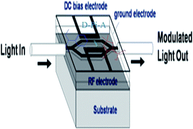
EO modulators encode electrical signals onto fiber optic transmission lines. The simplest kind of EO modulator usually uses inorganic crystals, like lithium niobate (tantalite), KH2PO4, TeO2, whose refractive index is changed under an applied dc or low frequency electric field strength. A high-performance laser modulator with 2.5 ns switching time based on CMOS-compatible technology of hydrogenated amorphous silicon (a-Si:H) has been fabricated, but crucial half-voltage magnitude VπL was very large (40 V cm).4 With respect to the above mentioned EO modulator's materials, polymer-based EO compounds possess capable of even faster EO response and negligible velocity mismatch between the optical and RF waves due to extremely low dielectric constant dispersion.
![]() | (1) |
Following the eqn (1), due to the close values of refractive indices between the microwave and optical waves, the modulation bandwidth of the polymer EO modulators will be much larger with respect to traditional inorganic materials (LiNbO3, LiTaO3, KNbO3 etc.) The high speed modulation limit of the material can be determined by the bandwidth-length product f × l, giving the maximum modulation frequency f, for a device of length L. As an example for LiNbO3 f × l ≅ 9.6 GHz cm in a standard Mach–Zehnder configuration, while for organic poled polymer films f × l ≅ 150 GHz cm.5
Another advantage of polymer EO modulators with respect to all other compounds is their lower Vπ. The EO tensor coefficients of several kinds of EO polymers have huge magnitudes-up to 200 pm V−1, which are almost 10 times higher than the analogous magnitude for lithium niobate crystal. This is a consequence of the phonon system contribution. For such kind of compounds it is substantially higher with respect to the inorganic ones and an harmonic phonons described by third rank polar tensors will be here more crucial.6,7
As shown from eqn (2), the Vπ is inversely proportional to the electro-optic tensor coefficients (r33). During development of EO polymers, Vπ will become substantially lower.8
![]() | (2) |
It is necessary to emphasize that the polymer EO Pockels materials have other advantages. For example, easier integration with other semiconductor devices, lower prices of the materials, simpler and chipper processing technology and so on. Unfortunately there remain still many problems to be solved. Among them – optimization of insertion loss, thermal stability, photochemical stability, time aging process, photothermal destruction and so on.
In the present short review, the structures and developing process for traditionally used NLO chromophores are reported, and the relationship between the development of polymer EO modulators and organic NLO chromophores is analyzed. According to the most principal characteristics of EO modulators (bandwidth, Vπ and insertion loss) they were used in different device architectures and different cladding materials like all polymer waveguide EO modulators, sol gel waveguide EO modulators and EO polymer–silicon hybrid modulator.9,10
r33 = 2Nf(ω)β〈cos3![]() | (3) |
In the first works, researchers paid much more attention to improve the chromophores' hyperpolarizability, and then to solve the problem of inter-molecular interactions in particularly with polymers for improving the content and polarization efficiency.16,17 A large amount of NLO chromophores were explored in the past decades. However, only few of them are widely used in EO devices fabrication. This is due to their comprehensive performances including EO efficiency, thermal stability, price and solubility. Chromophores which were widely used in the production of the EO devices and their EO coefficients are listed in Table 1.
The first used NLO chromophore for organic EO modulator was 4-dimethylamino-4′-nitrostilbene (DANS), with N,N-dimethylaniline as the donor group, nitrobenzene as the electron acceptor group and double-linked carbons as the electron bridge. Due to their short electron bridges and poor electron acceptors, they have shown only a small EO coefficient (6.1 pm V−1 at 1310 nm wavelength).18 Due to its small π-conjugated transport charge transfer length, this kind of chromophores has very high thermal stability, and it is easily to be attached to polymers.
Disperse red (DR) dyes are another kind of EO/NLO chromophores widely used in the preparation of organic EO modulators in the early days, due to their thermal stability and easy synthesis. The difference between DANS and DR in the electron bridge, nitrogen–nitrogen double bonds are used in DR instead of carbon–carbon double bonds in DANS. Because DR was widely used in printing and dyeing industry, and its price was very low, lots of EO polymers with disperse red as side chain were manufactured and studied in 90 s of the last century. Else, DR dyes also showed larger EO coefficients (about 15 pm V−1) than DANS.19
FTC chromophore with thiophene as the electron bridge and tricyano furan (TCF) as electron acceptor was synthesized and comprehensively studied in the end of last century. First order hyperpolarizability (1400 × 10−30 esu) at wavelength 633 nm was improved greatly in FTC chromophore, due to the large π-charge transfer and the acceptor's strong electron withdrawing ability.20–23 Its EO coefficients were studied in host–guest systems by incorporation in PMMA or APC polymer matrices, and a large EO coefficient of 58 pm V−1 was obtained at the wavelength of 1310 nm. Else, the parameters of chromophore FTC with respect to EO coefficient, possessed good orientation-aligned stability, optical loss, optical stability and thermal stability were intensively explored in recent years.24–28
Due to the strong stability and electron withdrawing ability of TCF electron acceptor, a large number of electron acceptors having the similar structure with TCF acceptor were synthesized in the early days of current century. Novel TCF acceptors with trifluoromethyl group was an outstanding one, trifluoromethyl group could both improve the electron withdrawing ability and reduce the optical absorption loss.29–33 Chromophore AJL8 using trifluoromethyl TCF acceptor possessed a large EO efficiency. Films of AJL8 doped in an amorphous polycarbonate matrix exhibit a very high r33 magnitude of 94 pm V−1 at 1310 nm.34
CLD chromophore is another kind of crucial NLO chromophore widely used in polymer EO devices. A ring-locked, phenyltetraene structure was used as the electron bridge, which had strong electron transfer ability and thermal stability.35 CLD1 with N,N-bis(2-(tert-butyldimethylsilyloxy)ethyl)aniline as electron donor and TCF acceptor has shown the largest EO coefficients of 120 pm V−1, which was almost two time larger with respect to FTC chromophore.36,37 Then a couple of CLD chromophores with larger EO coefficients were synthesized. Among them the most representative ones were AJSL102 and AJ309, prepared by Alex Jen research group in Washington University. Due to large isolated groups that were introduced to the electron acceptor, the chromophores' polarization efficiency was improved greatly, and the EO polymers using these chromophores showed us EO coefficients as large as 150 pm V−1 at 1310 nm.38,39
Afterwards, the polymer EO modulators and organic EO materials became the research hotspots and hundreds of research papers were published in this area. In 1992, Teng reported a design of traveling-wave electro-optic intensity modulator with a 3 dB electrical bandwidth with more than 40 GHz frequency using the same cladding and core materials. The excellent velocity matching between the optical and electrical waves in polymer materials was demonstrated.41
Wang et al. demonstrated the electro optic modulation up to 60 GHz using optical heterodyne technique for polymer waveguide phase modulators, which was manufactured by a cross-linked NLO polymer PUR-DR19 in 1995. And no fundamental material limitations in high frequency range for the used polymer materials were revealed.42
EO polymer modulators up to 113 GHz were successfully fabricated and characterized using poled PUR-DR19 as active core and Epoxylite 9653 as the claddings. The optical response variation for this device versus frequency over the whole band was varied up to 3 dB, as shown in Fig. 1.43
![]() | ||
Fig. 1 High frequency optical response curve of the polymer modulator from 74 to 113 GHz. The total variation was less than 3 dB (reproduced from ref. 42 with permission from the AIP publishing LLC). |
EO materials | Wavelength (μm) | Bandwidth (GHz) | Half-wave voltage (V) | Insert loss (dB) |
---|---|---|---|---|
DANS/PMMA | 1.55 | 5 | ||
PU-DR | 1.31 | 50–150 | 11 | |
PU-FTC | 1.31 | 40 | 3.6 | |
CLD1/APC | 1.55 | 20 | 1.8 | 11 |
AJL8 | 1.55 | 8 V | 14 | |
AJLS102 | 1.55 | 1.9 | 8 |
Half-wave modulation voltage as low as 3.7 and 4.8 V under 500 Hz operation was obtained by Lee et al. with a 1.5 cm long EO electrode at wavelengths of 1.3 μm and 1.55 μm, respectively. The EO polymer used in this work was the copolymer of methacrylate with dimethylaminonitrostilbene (DANS) polymers as a side chain and methylmethacrylate (MMA) (P2ANS/MMA (50/50); 50/50 means the molar ratio of DANS/MMA). Phenol resins were used as the lower and upper cladding materials, which were fabricated by the condensation reaction of phenol and formaldehyde. Due to the super high chromophore loading density, this EO modulator possessed Vπ below 5 V. Such high chromophore loading density means that the EO films have weak mechanical processing performance, large absorption loss and difficult to be aligned (poled).44
Oh et al. also paid their attention to reduction of half-wave voltage and they got the EO devices with half-wave voltage of 2.4 and 3.7 V at 1300 nm and 1550 nm, respectively.45 But they additionally paid much more attentions to the study of devices loss. The total insertion loss from the fiber output, through the device, and coupled to the detector was obtained to be 9–10 dB. Propagation losses measured using the high-index liquid immersion technique were found to be 1.2 dB cm−1 at 1300 nm and 2.0 dB cm−1 at 1550 nm for traditional all polymer EO materials. The results were among the best ones reported for polymer EO modulators using APC/CLD as core layer and UV15 as cladding layers.
In 2000, Shi el al firstly reported the polymer EO modulator with half-wave voltages of 0.8 V (at a telecommunications wavelength of 1318 nm) and they achieved a half-wave voltage-interaction length product equal to 2.2 V cm.46 Sterically modified organic chromophores for reduction of electric field attenuation in poling induced electro-optic activity possessed strong intermolecular electrostatic interactions. Optical push–pull poling and driving were used to reduce the half-wave voltage. Highly efficient optical push–pull modulator architecture (see Fig. 2) and CLD chromophores (see Table 1) were embedded to fabricate polymer EO modulator. Polyurethane films at wavelength 3.1 μm was used as lower cladding, 30 wt% CLD-1/PMMA films with 1.7 μm was used as guiding layer and Norland 73 layer of approximately 3 μm was spun and cured under ultraviolet light as the top cladding in this polymer EO modulator. Lower and upper claddings were almost the same like the traditional polymer modulators possessing low half-wave voltage due to the strong EO efficiency of guiding layer and the exceptionally efficient optical push–pull modulator architecture. Together with achievement of bandwidths more than 110 GHz and ease of integration (with very large scale integration semiconductor circuitry and ultra-low-loss passive optical circuitry) the latter confirm potential of polymeric materials for next generation of telecommunications, information processing, and radio frequency distribution.
![]() | ||
Fig. 2 Optical push–pull modulator architecture (reproduced from ref. 46 with permission from the American association for the advancement of science). |
After achievement of high frequency operation, low half-wave modulation voltage and acceptable insertion loss, researchers paid much more attentions to their commercial applications. According to the application in externally modulated CATV analog fiber-optic transmitters, the EO polymer modulators must survive an input optical power of 100–200 mW or higher for several years without any signs of degradation. Because the nonlinear optical chromophores are most sensitive to optical damage, the stable device operation requires that the chromophores will not be destroyed or reoriented by the intense many times infrared beam illumination and its higher order harmonic beams. Shi from TACAN corporation firstly reported the long term thermal stability and photochemical stability at 633 nm wavelength for double end crosslinked EO polymer modulators in 1997 possessing a cw optical power density of 1 mW cm−2 over extended periods of time with no increase in optical loss or decay in nonlinearity at 1.3 μm wavelength.47
The reliability of high speed polymer electro-optic (EO) modulators is the most critical milestone for the application of these materials in commercial applications. GigOptix Inc., presented thermal stability data for material and device level that proved the stability at 85 °C for 25 years of GigOptix' polymer modulators. Fundamentally, the reliability of the device materials is crucial for stable final devices. Thus the EO material's parameters were monitored from batch to batch after synthesis and during wafer fabrication. Key features at chip level were explored to have a performance distribution on a 6′′ wafer. Thermal study performed at chip level fitted using Jonscher model and was used to determine the isothermal aging stability of EO coefficient for 25 years and the EO materials activation energy. M3 EO material shows less than 10% variation in EO coefficient while operating at 85 °C for 25 years.48
The first hybrid EO polymer/sol–gel waveguide modulator, confining the EO polymers laterally in the sol–gel over cladding was fabricated by Enami in 2003 and is shown in Fig. 3. Its structure enables an adiabatic transition between the passive sol–gel waveguides and the active EO polymer overlayers without lateral radiation. Intensity is confined well in a 0.9 mm-thick EO Polymer overlayer, resulting in a lower Vπ due to the larger overlap integral. Through the half-wave voltage was still large (22 V), but it opens us a new way to improve the comprehensive performance of polymer EO modulator.53
![]() | ||
Fig. 3 Principal scheme of the hybrid EO polymer/sol–gel waveguide modulator (reproduced from ref. 53 with permission from the AIP publishing LLC). |
High efficient poling of electro-optic polymers is reported using an organically modified sol–gel cladding layer. This poling technique has resulted in a Pockel's coefficient enhancement of up to 2.5 times, (increasing from 26 pm V−1 when poled without a sol–gel cladding to 65 pm V−1), when optimally poled with a sol–gel cladding.54 Hybrid EO polymer/sol–gel modulators with low half-wave voltage and low insertion loss was reported by Enami et al. Larger EO tensor coefficient r33 is caused by the higher poling field and is achieved when EO polymer is sandwiched between sol–gel cladding layers. The reduced inter-electrode distance resulting from the elimination of the sol–gel core layer in the active region additionally reduces half-wave voltage. Straight channel phase modulators operates with Vπ = 4.2 V at 1550 nm using a reduced d of 11.5 μm, which corresponds to a r33 of 78 pm Vc. The latter is the highest r33 among the reported. A Mach–Zehnder modulator with Vπ = 3.9 V using a conventional d of 15 μm was also examined.55
Hybrid cross-linked electro-optic polymer/sol–gel Mach–Zehnder waveguide modulator with a Vπ of 0.65 V at = 1550 nm was designed in 2007. Such voltage is the lowest Vπ reported until now.57 The lower Vπ was achieved due to the following factors: (1) combination of both physical vertical tapers in the sol–gel core and photo bleached index tapers in the EO polymer; (2) reduction the thickness of the device up to 8 μm, as shown in Fig. 4. These combined physical and index tapers result in improved optical mode confinement in the EO polymer with low adiabatic optical transition loss. The reduced thickness results in a larger field across the EO polymer for the same voltage, enabling a lower Vπ.
![]() | ||
Fig. 4 Schematic schema of the sol gel hybrid waveguide modulator (reproduced from ref. 57 with permission from the AIP publishing LLC). |
Due to the advantages in VπL and bandwidth magnitudes, researchers have paid more and more attentions to the this kind of EO devices in the recent years.74–80 In 2008, Tom Baehr-Jones et al. reported an EO modulator fabricated from a silicon slot waveguide and clad made of nonlinear polymer YLD_124. The VπL for this modulator was calculated to be equal to 0.5 V cm and the Vπ was about 0.25 V with the r33 magnitude of the polymer equal to 30 pm V−1.67 Although the r33 magnitude was much lower than the optimal value of YLD_124 (100 pm V−1), almost the lowest Vπ was still achieved, which strongly supported the low driven power superiority of the silicon slot waveguide with EO polymer. In 2010, the same workgroup reported design of the first high speed polymer–silicon hybrid modulator with a bandwidth of 3 GHz and a VπL figure of merit equal to 0.8 V cm, which was fabricated of a silicon slot waveguide and clad consisting of AJSP100. High speed modulation was achieved by appropriately increase of thickness and doping of the strip-loading silicon.68 The first polymer–silicon hybrid modulator with a frequency bandwidth of 100 GHz was realized using a gate voltage, demonstrated by Luca Alloatti et al. in 2014 using the nonlinear polymer M3 with a r33 equal to 18 pm V−1 and the VπL of the modulator equal to 11 V cm.73
Fig. 5 illustrates the structure and the optical modes of the slot waveguide.81 Both the width and the distance between two silicon ridges are of the order of nanometers. Based on Maxwell's equation, the optical field is mainly concentrated in the low-index EO polymer materials between the high-index silicon due to the dielectric discontinuity.82
Besides, the silicon ridges can also act as a pair of very closely spaced but electrically isolated and optically transparent electrodes. The applied voltage across the narrow slot yields a very high electric field at low voltage, which is located exactly at the same place of the high optical field. Thus the overlap between the electric field and the optical field is very efficient. Furthermore, the intensities of both the electric field and the optical field in the nanometer slot are at higher possible levels that cannot be achieved with traditional modulators. So the EO polymer–silicon slot waveguide is very promising to fabricate low VπL modulators.
Fig. 6 presents the typical scheme of Mach–Zehnder interferometer based on the EO polymer–silicon slot waveguide. To be applied to high-speed operation, travelling electrodes made of metal material are still required because the resistance of thin silicon layers is too high to transmit microwave signals at any distance. As we know, the metal electrodes cannot directly touch the waveguides otherwise they will cause optical loss. So a thinner silicon layer is used to connect the metal electrodes to the slot waveguides, which ensures electrical conduction and optical isolation simultaneously, as shown in Fig. 6.83 Another method to connect the metal electrodes and the optical waveguide is a use a series of small silicon arms, as shown in Fig. 7.84 To prevent additional optical losses induced by mode distorting, the dimensions of the arms and the periodicity must be properly designed.85
![]() | ||
Fig. 6 (a) Typical scheme of Mach–Zehnder interferometer modulator based slot waveguide, (b) cross-sectional view of the silica–organic hybrid waveguide. |
![]() | ||
Fig. 7 Segmented silicon arms used to connect the electrode and the slot optical waveguide (reproduced from ref. 84 with permission from the AIP publishing LLC). |
Co-planar electrodes are usually used to drive the EO polymer–silicon hybrid modulators, which are conveniently linked not only to microwave signals but also to DC poling voltage. Fig. 8 shows the principal wire scheme. During poling operation, contact A and C are connected to the ends of a DC power source. Contact C defines a voltage of Vpoling, contact B – a voltage of Vpoling/2, and contact A is held at ground, leading to same poling effect in the two arms. During device operation, contact B is driven at the desired voltage, while contacts A and C are both held at ground, leading to opposite electric field direction in two arms and resulting into a push–pull operation.86 To achieve larger modulation bandwidth, an external DC gate voltage is applied to induce a highly conductive electron accumulation layer and reduce the resistance of the silicon strip-load with little optical losses. The limiting frequency of the modulator fRC = 1/(2πRC) increases with increasing gate voltage and the modulation bandwidth is limited only by propagation loss of the microwave signal along the travelling electrodes.87
Despite the silicon–polymer slot waveguide modulator shows great potential in low power and high speed modulation, poling efficiency, coupling with fiber, however losses are main obstacles for future practical applications. The highest in-device r33 of EO polymers in polymer–silicon slot waveguides is limited to value of 59 pm V−1. When coupling with fiber, gratings are required because of large mode field mismatch. Optical propagation loss is around 30 dB cm−1 for most slot waveguides without coupling loss. To solve the above-mentioned difficulties, Enami et al. suggested to use TiO2 multilayer films to substitute silicon as the slot waveguide core materials. The VπL of the polymer/TiO2 multilayer slot waveguide modulator was about 3.25 V cm and the propagation loss was estimated to be equal to 12–13 dB cm−1 which would be further reduced to 5 dB cm−1 after optimizing for straight channel slot waveguide. This slot waveguide approach was expected to reduce the Vπ and optical insertion loss while maintaining a large 3 dB bandwidth.88
Compact and low-power band-engineered EO polymer refilled silicon slot photonic crystal waveguide (PCW) modulator was also designed and demonstrated in 2014. The EO polymer was engineered for large EO activity and near infrared transparency. A PCW step coupler was used for optimization of coupling to the slow-light mode of the band engineered PCW. The half-wave switching-voltage was measured to be Vπ = 0.97 ± 0.02 V with the interaction length of 300 μm, corresponding to the r33 equal to 1190 pm V−1 and VπL of 0.291 ± 0.006 V mm in a push–pull configuration. Excluding the slow-light effect, we evaluate the EO polymer is poled with an efficiency of 89 pm V−1 in the slot.89
As shown in Fig. 9, a plasmonic-hybrid-waveguide-based optical phase modulator proposed and analyzed by Zhou is based on the field enhancement in the low-index high-nonlinear polymer layer providing nanoscale optical confinement and a fast optical modulation speed. At 2.5 V drive voltage, a π phase shift can be obtained for a 13 μm-long plasmonic waveguide. Because of its small capacitance and parasitic resistance, the modulation bandwidth could reach up to 100 GHz with a low power consumption of 9 fJ bit−1. Additionally, the plasmonic waveguide was connected to a silicon wire waveguide via an adiabatic taper with a coupling efficiency of 91%.90
![]() | ||
Fig. 9 (a) Schematic perspective view of the modulator based on a hybrid plasmonic waveguide. (b) Cross-sectional view of the hybrid plasmonic waveguide. |
This journal is © The Royal Society of Chemistry 2015 |