
Enhanced field emission properties based on In–In2O3 composite nanopagodas
Sin-Hui Wanga,
Shin Liua,
Shoou-Jinn Chang*a,
Tsung-Ying Tsaia and
Cheng-Liang Hsu*b
aInstitute of Microelectronics & Department of Electrical Engineering, Center for Micro/Nano Science and Technology, Advanced Optoelectronic Technology Center, National Cheng Kung University, Tainan 701, Taiwan, Republic of China. E-mail: changsj@mail.ncku.edu.tw
bDepartment of Electrical Engineering, National University of Tainan, Tainan 700, Taiwan, Republic of China. E-mail: clhsu@mail.nutn.edu.tw; Fax: +886-6-2602305; Tel: +886-6-2606123 ext. 7785
First published on 3rd December 2014
Abstract
In–In2O3 composite nanopagodas demonstrate excellent field emission properties with an enhanced kinetics factor (saturation ratio). The turn-on fields and β of the In–In2O3 nanopagodas were 2.0 V μm−1 and 3590. The indium of the In–In2O3 nanopagodas accumulates electrons and forms electron tunnels, which enhances the field emission properties.
Introduction
Recently, In2O3 has attracted much attention due to its wide direct bandgap energy of 3.4–3.8 eV,1,2 and it is now widely used in field emission, gas sensors and solar cells.3–5 It is well known that the optical and electronic properties of metal oxide semiconductors can be modulated by varying the morphology or doping with a variety of elements. For the morphology of In2O3, various one-dimensional (1D) In2O3 nanostructures have been synthesised, including nanotubes, nanowires (NWs), nanobelts and nanorods, etc.6–81D nanostructures (NSs) have attracted considerable interest for their potential application in field emission (FE) because of their sharp tips and high aspect ratios, which cause their high field enhancement factors (β).9 Li et al. reported electric-field-aligned vertical and random growth of In2O3 NWs.10 Kar et al. reported nanopyramids, nanocolumns and NWs of In2O3.11 Thus, investigation of the FE properties of In2O3 1D nanoforms is a key factor.
According to Huang et al., four kinds of novel layered In2O3 NS were synthesized by controlling the kinetics factor (saturation ratio).12 In this paper, two kinds of In2O3 NS were synthesized by changing the direction of the substrate. In addition, by decreasing the distance between the metal source and the substrate, we demonstrate the first successful fabrication of In–In2O3 conformable nanopagodas (NPs). The FE properties of the In–In2O3 NPs was better than those of In2O3 NWs.
Experimental
A 500 nm-thick silicon dioxide (SiO2) insulating layer was deposited onto a Si (111) substrate by wet oxidation. A 3 nm-thick Au film as the catalyst layer was deposited onto the SiO2/Si substrate using an electron-beam evaporator. Thermal vapor deposition was performed for the vapor–liquid–solid (VLS) growth of the In2O3 NSs. About 0.3 g of In powder (99.993%) was poured into an alumina bowl. The bowl, filled with powder, was placed in the center of an alumina boat. The Au/SiO2/Si substrate was placed next to the alumina bowl, and the substrate that was positioned upon the alumina boat was reversed. The argon flow rate was maintained at 54.4 sccm and the oxygen flow rate was 0.3 sccm. During the growth of In2O3, the quartz tube pressure, growth temperature, and growth time were maintained at 8 Torr, 1000 °C, and 30 min, respectively. For an enhanced saturation ratio, we changed the placement of the substrate beside and upon the indium metal source bowl in a horizontal quartz furnace.The morphologies and size distributions of the as-grown In2O3 NSs were characterized using a field-emission scanning electron microscope (FESEM) (JSM-7000F), which was operated at 10 keV. The crystallographic and structural properties of the as-grown In2O3 NSs were then determined using a MACMXP18 X-ray diffractometer. The field emission (FE) properties of these In2O3 NSs were measured at room temperature in a vacuum chamber at a pressure of 4 × 10⁻⁶ Torr. During the FE measurements, the anode was a tungsten probe with a diameter of 1.8 mm, while the inter electrode distance (d) between the anode and the In2O3 NSs was precisely maintained at 150 μm. A lamp was placed above the Si substrate as an excitation source for the In2O3 NSs. The current–voltage (I–V) characteristics were determined using a Keithley 237 high-voltage source and measuring unit, which measured in femtometers and provided a maximum voltage of 1000 V. The FE properties were extracted from the obtained I–V curves using the Fowler–Nordheim (F–N) model.
Results and discussion
Fig. 1(a) shows a cross-sectional FESEM image of the front of the Au/SiO2/Si substrate with the morphology of In2O3 NWs. The diameter and length of the In2O3 NWs were 100 nm and 12–18 μm. To enhance the vapor pressure of the metal, we reversed the location of the substrate above the indium power, and got the In–In2O3 NPs, as shown in Fig. 1(b). The diameter and length of the In–In2O3 NPs were 0.1–1 μm and 3–6 μm. According to the energy-dispersive X-ray (EDX) spectrum of the In2O3 NWs and In–In2O3 NPs, the In![[thin space (1/6-em)]](https://www.rsc.org/images/entities/char_2009.gif) :O ratios were 1.8:3 and 2.3:3, as shown in Fig. 1(c) and (d). This showed that the content of In in the In–In2O3 NPs was higher than that in the In2O3 NWs.
:O ratios were 1.8:3 and 2.3:3, as shown in Fig. 1(c) and (d). This showed that the content of In in the In–In2O3 NPs was higher than that in the In2O3 NWs.
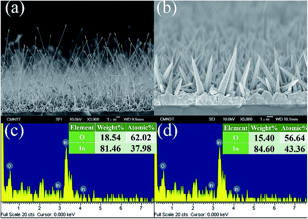 | ||
| Fig. 1 FESEM images and EDS of In2O3 NSs synthesized at 1000 °C with the position of the substrate ((a) and (c)) beside and ((b) and (d)) upon the precursor. | ||
Lattice structure analysis was performed using XRD measurements. Fig. 2 shows the XRD 2θ-scan spectra. The black line represents the XRD result of the In2O3 NWs we synthesized before and reveals a body-centred cubic (bcc) structure with a lattice constant of a = 10.09 Å, as characterized by JCPDS card no. 65-3170. Other peaks that are also assigned to the In2O3 structure according to the JCPDS database are present and indicated in the spectrum. These weaker peaks were thought to be the result of thin layers or particles depositing on the surface during the initial growth process. The red line represents the XRD result of the In–In2O3 NPs. The (222) peak is strengthened in In–In2O3 NPs. The noticeable strengthening of the (222) peak is ascribed to lateral 0-D growth of the In–In2O3 NPs, as described in the previous growth process. As shown in the spectra, the other difference is that there is a peak assigned to pure indium by JCPDS card no. 85-1409. Indium metal really existed in the In–In2O3 NPs, and it is worth pointing out that the other peaks present for the In–In2O3 NPs have no shift compared with the database, which leads us to the conclusion that the In2O3 NPs fabricated in this study are characteristic of the fine crystal structure.
 | ||
| Fig. 2 X-Ray diffraction spectra for the In2O3 NWs and In–In2O3 NPs. | ||
During the production process of the In2O3 NWs, the substrate was placed next to the indium powder boat, and the Au film on the SiO2/Si substrate would form Au nanoparticles at around 500 °C. The Au nanoparticles acted as the catalysts for VLS growth. Due to the large amount of indium vapor reacting with oxygen, the oxidized indium vapors had a large supersaturation ratio. Research has shown that the supersaturation ratio is inversely proportional to the critical core radius.13 Additionally, eutectic droplets acted as absorption sites for the oxidized indium vapors and confined these precipitates to one-dimensional growth. At higher temperatures, indium vapors would be notably generated and abundant reagent species would be adsorbed onto the droplets. This could lead to the rapid precipitation of solid In2O3 NSs, and the reaction would take place at the liquid–solid interface maintaining the 1-D growth.
The synthesis of the In–In2O3 NPs during the growth process was carried out as illustrated in Fig. 3, and three different mechanisms were ascribed to the formation of the In–In2O3 NPs.
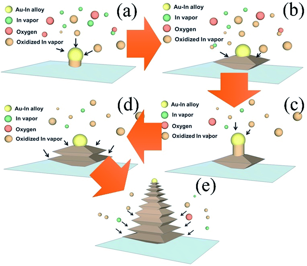 | ||
| Fig. 3 Growth process of In–In2O3 NPs. | ||
(I) To begin with, with the evaporation of liquid indium, some indium vapors would directly deposit and alloy with the Au nanoparticles before oxidizing due to the short distance between the substrate and the precursor. As a result, the composition of the eutectic droplet would mainly be indium, which plays a catalytic role in the growth mechanism. The abundant In vapors react with oxygen as the temperature rises and continuously dissolve into the alloy droplet. Once the vapor pressure of these adsorbed species in the droplet reaches supersaturation vapor pressure, the consequent 1-D growth mechanism of solid-state In2O3 would start, as shown in Fig. 3(a).
(II) As the growth time increases, the gradual decrease in the saturation ratio of the reagent species would slow down the rate of 1-D growth. It is at this stage that the continuous indium vapor that evaporates from the precursor would be oxidized and adsorbed onto the surface of the 1-D In2O3 NS. Considering the low saturation ratio of the adsorbed species in the droplet, this is too low to maintain the mechanism of 1-D growth. As a result, these abundant oxidized indium vapors would favor 0-D growth, followed by a vapor–solid (V–S) mechanism.14 Subsequently, lateral growth would carry on, as shown in Fig. 3(b).
(III) During the 0-D growth process, there were some oxidized indium vapors dissolved into the catalytic droplet at the top. Moreover, the reagent species adsorbed on the lateral surface might also have diffused into the droplet. As a result, the saturation ratio would rise gradually and reach the supersaturation vapor pressure. The VLS mechanism then dominated the growth process once again. As a result, most of the adsorbed species would transfer to maintain the 1-D growth, as Fig. 3(c) shows.
(IV) Again, if the saturation ratio was gradually lowered, it would convert back to the 0-D growth mechanism as described in step II, and lateral growth would restart as shown in Fig. 3(d). Based on the varied saturation ratio of the droplet, the whole growth process showed a competitive phenomenon between longitudinal 1-D growth and radial 0-D growth, as shown in Fig. 3(e). It is worth mentioning that even when 1-D growth was dominant there were still some reagent species diffusing to the lateral surface. Consequently, this caused uninterrupted lateral growth during the whole growth process, so if the lateral layer of the NPs was closer to the bottom it would have a large diameter because of the longer growth time.
Fig. 4 plots the FE current density (J) of the In2O3 NWs as a function of the applied electric field (E). The turn-on field (Eto) is defined as an electric field producing a current density of 10 μA cm−2. The Eto of the In2O3 NWs and In–In2O3 NPs are 2.9 and 2.0 V μm−1. The ln(J/E2) was plotted as a function of 1/E in the F–N plot in the inset of Fig. 4. The FE properties were analyzed by F–N theory to understand the emission characteristics, using the following equation:

which could be used to calculate the field enhancement factor or the work function. Assuming that the work function is 5.0 eV for In2O3, the field enhancement factor of the In2O3 NWs was estimated to be about 2123. When the saturation ratio increased, the In2O3 NS transformed into In–In2O3 NPs and the value of β was enhanced to 3590.

 | ||
| Fig. 4 The J–E field emission plots of the In2O3 NWs and In–In2O3 NPs. The inset displays the F–N plots of ln(J/E2) versus 1/E. | ||
In Table 1, the In2O3 nanotowers displayed the highest Eto value, which was dependant on the tip diameter.18 Lin et al. reported that β values are related to the emitter geometry, crystal structure, vacuum gaps, and spatial distribution of the emitting centers.21 This shows that β obviously depends on d, with a relationship of 1/β being proportional to 1/d. According to the above two viewpoints, in this work, the Eto and β values of the In2O3 NWs and In–In2O3 NPs are lower and higher than those in the references in Table 1. However, the In2O3 NWs and In–In2O3 NPs in this report have the same tip diameter and d, so the metal indium in the In–In2O3 NPs must enhance the transmission of electrons.
| Material | Length (μm) | Tip diameter (nm) | d (μm) | Eto (V μm−1) | β | Ref. |
|---|---|---|---|---|---|---|
| In–In2O3 nanopagodas | 3–6 | 100 | 150 | 2.0 | 3590 | This work |
| In2O3 nanowires | 12–18 | 100 | 2.88 | 2123 | ||
| In2O3 nanoneedles | 2 | 50 | 300 | 4.9 | 3695 | 18 |
| Nanohooks | Several tens | 50 | 7.5 | 1770 | ||
| Nanorods | Several tens | 125 | 7.7 | 1374 | ||
| Nanotowers | Several tens | 300 | 9.5 | 458 | ||
| In2O3 nanotrees | Several tens | Few micrometers | 220 | 6.45 | 1993 | 19 |
| Nanopins | >300 | 1000 | 4.58 | 2320 | ||
| Nanobrushes | >400 | 600 | 3.94 | 2749 | ||
| Sn–In2O3 nanowires | 5 | 50 | — | 6.6 | 1857 | 20 |
| In2O3 nanowires – Ga2O3 nanobelts | 60 | 300 | 170 | 4.23 | 1142 | 21 |
Fig. 5(a) schematically depicts the band diagrams of the tips of the In2O3 NWs. In2O3 is an n-type material. The Fermi level (Ef) of the depletion region was close to the conduction band Ec. When in a high electric field, the conduction band bends to Ef, and the electrons will tunnel to the vacuum level. In accordance with the indium metal enhancing the FE performance, the band diagrams of the In–In2O3 NPs are shown in Fig. 5(b). In Fig. 5(c), the electrons came from electrical power and were then transported from the In2O3 NPs to the metal In region. The In clusters of the In2O3 NPs assembled many transfer paths for enhanced conductivity. Ultimately the electrons were collected at the Au–In alloy nanoparticles (the tips of the In–In2O3 NPs) by the electric field effect. The work functions of In2O3, Au and In are 5.0 eV, 5.1 eV and 4.0 eV, respectively.22 The tunnelling of electrons from the In region to the vacuum level will be easier than for Au and In2O3. The enhanced FE properties of the In–In2O3 NPs come from the In cluster assembled conduction paths and reduced work function (Φ). This work reveals the lowest Eto and the best FE performance compared with past In2O3 nanostructure reports.
 | ||
| Fig. 5 Band diagrams of (a) the In2O3 NWs and (b) the In–In2O3 NPs. (c) A schematic diagram of the electronic transmission channel in the In–In2O3 NPs. | ||
Conclusions
The morphology of In2O3 NSs was transformed from NWs into NPs when the In vapor pressure increased. The In–In2O3 conformable NPs were synthesized with ultrahigh concentrations of indium vapor. The turn-on fields of the In2O3 NWs and In–In2O3 NPs were 2.9 and 2.0 V μm−1, respectively. The In–In2O3 NPs had an increased β value of 3590, and the β of the novel In2O3 NWs was 2123. The In clusters in the In–In2O3 NPs act as electron transmission channels and FE emitters due to their lower work function (Φ). The In–In2O3 NPs present the best FE properties of the In2O3 NSs reported, and they are a suitable candidate for FE sensitive switching elements in nanoelectronic device applications.Acknowledgements
The authors would like to thank the Ministry of Science and Technology of the Republic of China, Taiwan, for financially supporting this research under Contract no. MOST 103-2221-E-024-016.Notes and references
- H. A. R. Aliabad, Y. Asadi and I. Ahmad, Opt. Mater., 2012, 34, 1406 CrossRef PubMed.
- Y. Fan, M. Jin, F. Xianjin and K. Lingyi, J. Cryst. Growth, 2008, 310, 4054 CrossRef PubMed.
- S. Q. Li, Y. X. Liang and T. H. Wang, Appl. Phys. Lett., 2005, 87, 143104 CrossRef PubMed.
- P. S. Khiabani, E. Marzbanrad, H. Hassani and B. Raissi, J. Am. Ceram. Soc., 2013, 96, 2493 CrossRef CAS PubMed.
- D. H. Kim, S. Lee, J. H. Park, J. H. Noh, I. J. Park, W. M. Seong and K. S. Hong, Sol. Energy Mater. Sol. Cells, 2012, 96, 276 CrossRef CAS PubMed.
- L. Xu, B. A. Dong, Y. Wang, X. Bai, Q. Liu and H. W. Song, Sens. Actuators, B, 2010, 147, 531 CrossRef CAS PubMed.
- G. Z. Shen, J. Xu, X. F. Wang, H. T. Huang and D. Chen, Adv. Mater., 2011, 23, 771 CrossRef CAS PubMed.
- J. Yang, C. K. Lin, Z. L. Wang and J. Lin, Inorg. Chem., 2006, 45, 8973 CrossRef CAS PubMed.
- K. F. Huo, X. M. Zhang, L. S. Hu, X. Sunl, J. Ful and P. K. Chu, Appl. Phys. Lett., 2008, 93, 013105 CrossRef PubMed.
- S. Q. Li, Y. X. Liang and T. H. Wang, Appl. Phys. Lett., 2005, 87, 143104 CrossRef PubMed.
- S. Kar, S. Chakrabarti and S. Chaudhuri, Nanotechnology, 2006, 17, 3058 CrossRef CAS.
- Y. Huang, K. Yu, Z. Xu and Z. Zhu, Phys. E, 2011, 43, 1502 CrossRef CAS PubMed.
- Y. Hao, G. Meng, C. Ye and L. Zhang, Cryst. Growth Des., 2005, 5, 617 Search PubMed.
- Y. G. Yan, Y. Zhang, H. B. Zeng and L. D. Zhang, Cryst. Growth Des., 2007, 7, 940 CAS.
- R. H. Fowler and L. Nordheim, Proc. R. Soc. London, Ser. A, 1928, 119, 173 CrossRef CAS.
- C. J. Edgcombe, Philosophical Magazine Part B, 2002, 82, 1009 CAS.
- V. Filip, D. Nicolaescu, M. Tanemura and F. Okuyama, Ultramicroscopy, 2001, 89, 39 CrossRef CAS.
- B. Wang, X. Jin, Z. B. Ouyang and P. Xu, J. Nanopart. Res., 2012, 14, 1008 CrossRef.
- Y. Wang, Y. Li, K. Yu and Z. Zhu, J. Phys. D: Appl. Phys., 2011, 44, 105301 CrossRef.
- B. Wang, Z. Zheng, H. Wu and L. Zhu, Nanoscale Res. Lett., 2014, 9, 111 CrossRef PubMed.
- J. Lin, Y. Huang, Y. Bando, C. C. Tang, C. Li and D. Golberg, ACS Nano, 2010, 4, 2452 CrossRef CAS PubMed.
- S. Kar, S. Chakrabarti and S. Chaudhuri, Nanotechnology, 2006, 17, 3058 CrossRef CAS.
| This journal is © The Royal Society of Chemistry 2015 |