Defect driven ferromagnetism in SnO2: a combined study using density functional theory and positron annihilation spectroscopy

A. Sarkara, D. Sanyal*b, Palash Nathc, Mahuya Chakrabartic, S. Palc, S. Chattopadhyayd, D. Janac and K. Asokane
aDepartment of Physics, Bangabasi Morning College, 19 Rajkumar Chakraborty Sarani, Kolkata 700009, India
bVariable Energy Cyclotron Centre, 1/AF, Bidhannagar, Kolkata 700064, India. E-mail: dirtha@vecc.gov.in; Fax: +91-33-23346871; Tel: +91-33-23184462
cDepartment of Physics, University of Calcutta, 92 Acharyya Prafulla Chandra Road, Kolkata 700009, India
dDepartment of Physics, Maulana Azad College, 8 Rafi Ahmed Kidwai Road, Kolkata 700013, India
eInter University Accelerator Centre, Post Box 10502, Aruna Asaf Ali Marg, New Delhi 110067, India

Received 2nd October 2014 , Accepted 14th November 2014

First published on 14th November 2014


Abstract

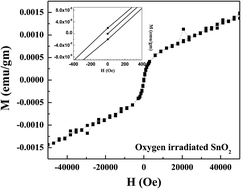
Room temperature ferromagnetic ordering has been observed in a high purity polycrystalline SnO2 sample due to irradiation of 96 MeV oxygen ions. Ab initio density functional theory calculation indicates that tin vacancies are mainly responsible for inducing the magnetic moment in SnO2 whereas oxygen vacancies in SnO2 do not contribute any magnetic moment. Positron annihilation spectroscopy has been employed to characterize the chemical identity of irradiation generated defects in SnO2. Results indicate the dominant presence of Sn vacancies in O ion irradiated SnO2. The irradiated sample turns out to be ferromagnetic at room temperature.


1. Introduction

Defects are ubiquitous in solids. An insignificant amount of defects in a solid can significantly alter its electrical, optical and magnetic properties. In fact, defect induced ferromagnetism in a wide range of materials has become one of the most discussed issues in the recent past.1–4 In oxide semiconductors like ZnO and other related compounds, several defect configurations offer enormous possibilities to study defect induced phenomenon theoretically and experimentally.5,6 The majority of scientific efforts have been directed to find ferromagnetism in doped and undoped ZnO7–9 whereas, relatively fewer investigations exist on similar other materials like TiO2 (ref. 10 and 11) and SnO2.12,13 The present theoretical and experimental work has been focused to investigate the role of defects in generating ferromagnetism in SnO2. SnO2 is a wide band gap (∼3.6 eV at room temperature) n-type semiconductor. In recent times, the occurrence of room temperature ferromagnetic ordering in undoped SnO2 has been reported.14–17 Espinosa et al. have indicated15 that Sn vacancy (VSn) is responsible for inducing ferromagnetism in SnO2 while Chang et al. favored16 the key role of oxygen vacancies (VO) for the same. Yuan et al. have found17 that vacancy defects at grain surfaces in nanocrystalline SnO2 control saturation magnetization (Ms). In SnO2 nanowires, strong and tunable ferromagnetic response by ultraviolet light irradiation has been observed.18 In the present effort, first principles DFT calculation has been adopted to observe the effect of VSn and VO on the electronic structure of SnO2. DFT results predict that VSn are responsible for inducing ferromagnetism in SnO2. On the experimental side, defects in SnO2 have been created by 96 MeV oxygen beam irradiation. Positron annihilation spectroscopic (PAS) investigation reveals the abundance of Sn vacancies in the irradiated (ferromagnetic) material. It is worth mentioning that PAS spectroscopy is very much sensitive to vacancy type open volume defects in solid materials.2,6,19 Particularly, in oxide semiconductors like ZnO and related materials, it efficiently probes cation vacancies with sub ppm accuracy.20

Doppler broadening of the electron-positron annihilation radiation line shape (DBEPARL) measurement technique is useful to study the momentum distribution of electrons in a material. Depending on the electron momentum (p), the 511 keV γ-rays (electron-positron annihilated) are Doppler shifted by an amount ±ΔE = pLc/2 in the laboratory frame, where pL is the component of the electron momentum (p) along the direction of measurement.19 Using high energy resolution HPGe (high purity germanium) detectors, one can measure the Doppler shift of the 511 keV γ-ray spectrum. In this spectrum, the region away from 511 keV photo peak is formed due to annihilation of positrons with higher momentum core electrons of the constituent atoms of the sample. Energy (or momentum) of such core electrons are element specific. So by analyzing the DBEPARL spectrum, identification of the vacant atomic sites can be done. But due to large background in the γ-ray spectrum the analysis of high pL region becomes cumbersome and ambiguous. Use of the two detectors in coincidence (henceforth will be called CDBEPARL technique) is necessary to suppress the background in measured Doppler broadened spectrum and the contributions of higher momentum core electrons in the spectrum can be estimated.2,19,20

2. Experimental outline

As received 99.996% pure (Alfa Aesar, Johnson Mathey, Germany) SnO2 powder has been used in this work. The powder has been pelletized and annealed at 700 °C before irradiation.

The magnetization measurements were done in a MPMS-XL SQUID (superconducting quantum interference device; Quantum Design) magnetometer.

For CDBEPARL measurement, 10 μCi 22Na source of positrons (enclosed between ∼1.5 μm thin nickel foils) has been sandwiched between two identical pellets. Electron-positron annihilated 511 keV gamma ray line shape measurements have been carried out using two identical HPGe detectors (efficiency: 12%; type: PGC 1216sp of DSG, Germany) having energy resolution of 1.1 keV at 514 keV of 85Sr. CDBEPARL spectra have been recorded in a dual ADC based – multiparameter data acquisition system (MPA-3 of FAST ComTec., Germany) having energy per channel −146 eV. The peak to background ratio of this measurement system with ±ΔE selection is ∼105[thin space (1/6-em)]:[thin space (1/6-em)]1. The CDBEPARL spectrum has been analyzed by evaluating the ratio curve analysis.19,20 In each CDBEPARL spectrum the S-parameter19 is calculated as the ratio of the counts in the central area of the 511 keV photo peak (|511 keV − Eγ| ≤ 0.85 keV) and the total area of the photo peak (|511 keV − Eγ| ≤ 4.25 keV). Defects in SnO2 were created by using 96 MeV 16O8+ ions from 15 UD pelletron at IUAC, New-Delhi. The irradiation fluence is 3.3 × 10¹³ ions per cm2. The beam is uniformly scanned on the sample area of 1 cm × 1 cm.

3. Theoretical methodology

Defect induced modification of magnetic property of the SnO2 have been investigated theoretically by studying the spin polarized density of states as calculated by the ab initio density functional theoretical approach.21–23

The theoretical calculations have been carried out in the frame work of the ab initio density functional theory using the code MedeA VASP24–27 based on linear basis set expansion. Super cell size is 2 × 3 × 3 i.e., 108 atoms are taken for simulation with periodic boundary condition along the lattice vectors. All the structures are geometrically relaxed through the conjugate-gradient algorithm until all the unbalanced inter atomic forces are converged below 0.02 eV Å−1. The unit cell size is obtained by geometrical optimization, which yields the lattice constant as, a = 4.7367 Å, b = 4.7367 Å and c = 3.1855 Å. All the simulations have been performed in the framework of generalized gradient approximation (GGA) with Perdew–Burke–Ernzerhof (PBE) exchange28 correlation. The energy convergence criteria have been set to the value 10−4 eV and with the energy cut-off value of 400 eV. For Brillouin zone (BZ) sampling the Monkhorst–Pack parameter29 are set by 3 × 2 × 3 k-points. The magnetic property of defect induced SnO2 has been carried out by considering the spin polarized DFT calculation. The spin degrees of freedom fully relaxed during the simulation until the system converge to the spin polarized ground state. No initialization has been taken into account for the spin magnetic moment of the atoms or defects of the considered system. To create the defective system, a single Sn atom is removed from the system of 108 atoms yielding a Sn vacancy (VSn) concentration ∼1.0% (Fig. 1) and similarly O atom also removed from the system to produce the O vacancy (VO). For further calculation regarding the magnetic coupling (ferromagnetic or antiferromagnetic) between the defects, two VSn are considered in the SnO2 system at a distance 4.74 Å apart from each other and then ferromagnetic and antiferromagnetic ground state have been predicted through spin polarized DFT.


image file: c4ra11658e-f1.tif
Fig. 1 Magnetization density of different SnO2 systems. (a) The pristine SnO2 structure showing no magnetism. (b) Oxygen vacancy (VO) in SnO2 system; (c) SnO2 system with single Sn vacancy (VSn); highly localized magnetization is noticed around Sn vacancy due to the nearest oxygen atoms. (d) Double Sn vacancy in SnO2 system, the nearest oxygen atoms give rise to local magnetism. In the figures (b)–(d) the dotted circles represents the vacancy sites.

4. Results and discussion

The pristine and irradiated samples show standard X-ray diffractogram patterns of SnO2 only (not shown). Little broadening of the diffraction lines due to irradiation has only been observed. The maximum penetration depth of 96 MeV O ions in SnO2 is 54.6 μm (estimated using SRIM30). The maximum electronic energy loss by 96 MeV O ion is in the hundreds of eV Å−1 range (Fig. 2). Such values are much lower than the typical columnar defect generation threshold in insulators.31,32 Thus, mostly point defects are generated in SnO2 by the 96 MeV O ions. In order to obtain the vacancy concentration, one has to specify displacement threshold energy in SRIM. To the best of our knowledge, there is no theoretical or experimental data for the displacement threshold energy (Ed) of Sn or O in SnO2. So in accordance with Ed values for Zn and O atoms in ZnO, these values have been taken as 57 eV (ref. 33). SRIM predicts 3VSn and 4VO in 2 × 10⁴ atoms for a fluence of 1014 ions per cm2. Due to such high concentration of defects, a significant modification of electronic properties is expected. However, it is to be noted that SRIM only predicts instantaneously generated defect concentration, no after-effect such as dynamic recovery or defect complex formation is beyond the scope of such calculation.
image file: c4ra11658e-f2.tif
Fig. 2 Electronic and nuclear energy deposition of 96 MeV O8+ on SnO2 as simulated by SRIM.

Fig. 3 show the M vs. H curve, measured at room temperature for the oxygen irradiated SnO2. The hysteresis loop (ferromagnetic ordering) at room temperature for the ion irradiated sample is relatively small (inset of Fig. 3) compared to the earlier experimental results on Ar irradiated TiO2 (ref. 10) or mechanically milled SnO2.34 The coercieve field is only 75 Oe as is seen from the inset of Fig. 3.


image file: c4ra11658e-f3.tif
Fig. 3 Room temperature magnetic hysteresis loop of 96 MeV O irradiated SnO2. The inset shows the enlarged part near the zero field region.

The spin polarized density of states, as calculated by the ab initio density functional theory, for the pristine SnO2, VO in SnO2 and VSn in SnO2 have been plotted in Fig. 4–6 respectively. The symmetric spin polarized (for the up-spin and down-spin) density of states as depicted in Fig. 4 clearly indicates that the pristine SnO2 yields zero magnetic moment. Due to the introduction of VO in SnO2 (Fig. 5) no magnetic moment have been emerged in SnO2, while the present calculation shows an asymmetric spin polarized density of states (DOS) for VSn, which results a non-zero magnetic moment of 3.63 μB (Fig. 6). It is quite interesting to note that this value is in close agreement as predicted by Rahman, et al.12 In particular, the strong asymmetry between spin up and down state in SnO2 with VSn exists very close to the Fermi energy (−2.5 eV to 0 eV). The defect formation energy of VSn and VO has also been evaluated from the MedeA VASP software using the following definition;

Ef = Ed + EaEp
where, Ef is the defect formation energy while Ed and Ep denote the total energy of the defective and pristine SnO2 structures respectively. Ea is the energy of isolated Sn or O atom for VSn and VO respectively. From the defect formation energy as shown in the Table 1, it can be concluded that the formation of VO is energetically favorable than the VSn. However, non-equilibrium processes like ion irradiation as done here, abundant VSn can also appear in the system.


image file: c4ra11658e-f4.tif
Fig. 4 Spin polarized density of states for non-defective SnO2 (Sn16O32).

image file: c4ra11658e-f5.tif
Fig. 5 Spin polarized density of states for SnO2 with oxygen vacancy (Sn16O31).

image file: c4ra11658e-f6.tif
Fig. 6 Spin polarized density of states for SnO2 with Sn vacancy (Sn15O32).
Table 1 Theoretically calculated parameters (using DFT) for the non-defective SnO2, oxygen vacancy (VO) incorporated SnO2, and tin vacancy (VSn) incorporated SnO2
System Defect formation energy (eV) Bond length (Å) Magnetic moment (μB)
Pristine 0.0 1.952 0.0
VO 8.69 1.842 0.0
VSn 16.0 1.884 3.63


To investigate the interaction between the magnetic moments for a fixed defect-defect distance, we have further carried out the calculations with the two magnetization configurations, e.g., ferromagnetic (FM) and antiferromagnetic (AFM) states, respectively. The distance between the two defect sites in the supercell is taken to be 4.74 Å. The atomic positions in both FM and AFM cases have been fully optimized and the total energy has been computed. It has been found that the FM state is the ground state and its energy is roughly ∼96 meV lower than that of the AFM state.

The implantation depth for the positrons from radioactive 22Na is given by P(x) = η[thin space (1/6-em)]exp(−ηx), where x is the distance measured from the surface of the sample from where the positrons penetrate inside the sample. 1/η is the characteristic penetration depth of a positron with specific energy (E). One can calculate 1/η which is approximately (Emax)1.4/16ρ in cm, if E is expressed in MeV and ρ is the density of the material in gm cm−3 (ref. 35). Emax is the maximum energy of the emitted positrons, e.g., for 22Na, Emax is ∼0.54 MeV. In SnO2 with density 5.56 gm cm−3 (taking 80% of the ideal density 6.95 gm cm−3 for porous sample), 1/η comes out to be ∼47 μm. It has been earlier mentioned that the depth of the irradiated region, as estimated by SRIM, is ∼54.6 μm. So majority of the positrons will annihilate in damaged region of the irradiated sample. It is well known that the so called S-parameter represents the annihilation fraction of positrons with low energy electrons.19,35 Increase of S-parameter represents enhanced positron annihilation at open volume defects. The S-parameter values of the pristine and irradiated materials are 0.5440 and 0.5457 respectively. Ratio curve analysis reveals that such open volumes in the irradiated sample are predominantly VSn type. Fig. 7 shows the area normalized ratio curve of the CDBEPARL spectrum of oxygen ion irradiated SnO2 with the same of pristine SnO2. The dip in the ratio curve at momentum (pL) value of 18 × 10−3m0c indicates less annihilation of positrons with the higher momentum core electrons of Sn. Assuming positrons are thermalized before annihilation and using Virial theorem approximation (in the atom the expectation value of the kinetic energy of an electron, Ekin, is equal to the binding energy of the electron), one can calculate the Ekin using pL = (2m0Ekin)1/2 (ref. 36). Here m0 is the rest mass of an electron. The dip position in the ratio curves correspond to Ekin = 82.8 eV. This value of Ekin nicely agrees with the binding energy of Sn 4p core electrons (∼83.6 eV).37 As a consequence, presence of stable Sn vacancies in the 96 MeV O irradiated SnO2 can now be concluded.


image file: c4ra11658e-f7.tif
Fig. 7 Ratio curve constructed from the CDBEPARL spectrum for irradiated SnO2 with respect to the same for pristine sample.

In the light of our results, decreasing trend of ferromagnetic moment with high temperature annealing14,17 of SnO2 nanoparticles can now be understood in the following way. Above 400 °C annealing grain boundary defects starts to recover and average grain size is increased.17,38 The situation of nano-SnO2 (ref. 38) is very similar to that of nano-ZnO.9,39 In both cases, cation vacancies at the grain surfaces start recovering above certain annealing temperature (300–400 °C). Of course, the concentration of singly ionized oxygen vacancies may also decrease14 due to high temperature annealing, however, our DFT calculations indicate that the primary reason for the decay of ferromagnetic moment is the decrease of VSn. In fact, as seen in ZnO, any extended disorder with several vacancy agglomerates either at grain boundaries40 or at irradiated regions7 can act as background defect network necessary for ferromagnetic interaction. Already it has been found that formation of VSn is more probable compared to VO in truncated SnO2 surfaces (as in nanosheets41). Similar phenomenon is very much likely in the vicinity of extended disorders in bulk SnO2. This contention fits well with the experimental report of increasing ferromagnetic moment of SnO2 powder34 with increasing hours of mechanical milling (which add net disorder in the system39). PAS results confirm the presence of cation vacancies in the core of such disorder, generated either by ion irradiation (as is here in O irradiated SnO2) or in mechanically milled ZnO.39 More investigation on the formation, chemical nature and role of vacancy clusters in SnO2 would be encouraging. Few days before the submission of this manuscript, another article42 combining theoretical and experimental investigation on nanocrystalline SnO2 shows remarkably similar results confirming the role of VSn defects/defect clusters for ferromagnetic interaction in the system.

5. Conclusion

Combining theoretical and experimental study, we have shown that occurrence of room temperature ferromagnetism in SnO2 is due to Sn vacancies. The present methodology will serve for a conclusive identification of chemical nature of open volume defects in oxide and other compound semiconducting materials.

Acknowledgements

P. Nath acknowledges the financial assistance from Council of Scientific and Industrial Research (CSIR), Govt of India. S. Pal acknowledges University Grants Commission (UGC), Govt of India for providing his RFSMS fellowship.

References

  1. A. Sundaresan, R. Bhargavi, N. Rangarajan, U. Siddesh and C. N. R. Rao, Phys. Rev. B: Condens. Matter Mater. Phys., 2006, 74, 161306(R) CrossRef.
  2. D. Sanyal, M. Chakrabarti, T. K. Roy and A. Chakrabarti, Phys. Lett. A, 2007, 371, 482 CrossRef CAS PubMed.
  3. M. Venkatesan, C. B. Fitzgerald and J. M. D. Coey, Nature, 2004, 430, 630 CrossRef CAS PubMed.
  4. A. Majumdar, S. Chowdhury, P. Nath and D. Jana, RSC Adv., 2014, 4, 32221 RSC; P. Nath, A. Chakraborti and D. Sanyal, RSC Adv., 2014, 4, 45598 RSC.
  5. J. Bang, Y. Kim, C. H. Park, F. Gao and S. B. Zhang, Appl. Phys. Lett., 2014, 104, 252101 CrossRef PubMed.
  6. S. Dutta, S. Chattopadhyay, A. Sarkar, M. Chakrabarti, D. Sanyal and D. Jana, Prog. Mater. Sci., 2009, 54, 89 CrossRef CAS PubMed.
  7. S. Mal, S. Nori, J. Narayan, J. T. Prater and D. K. Avasthi, Acta Mater., 2013, 61, 2763 CrossRef CAS PubMed.
  8. B. Sieber, J. Salonen, E. Makila, M. Tenho, M. Heinonen, H. Huhtinen, P. Paturi, E. Kukk, G. Perry, A. Addad, M. Moreau, L. Boussekey and R. Boukherroub, RSC Adv., 2013, 3, 12945 RSC.
  9. S. Ghosh, A. Sarkar, S. Chattopadhyay, M. Chakrabarti, D. Das, T. Rakshit, S. K. Ray and D. Jana, J. Appl. Phys., 2013, 114, 073516 CrossRef PubMed.
  10. D. Sanyal, M. Chakrabarti, P. Nath, A. Sarkar, D. Bhowmick and A. Chakrabarti, J. Phys. D: Appl. Phys., 2014, 47, 025001 CrossRef.
  11. M. Parras, Á. Varela, R. Cortés-Gil, K. Boulahya, A. Hernando and J. M. González-Calbet, J. Phys. Chem. Lett., 2013, 4, 2171 CrossRef CAS; S. Zhou, E. Čižmár, K. Potzger, M. Krause, G. Talut, M. Helm, J. Fassbender, S. A. Zvyagin, J. Wosnitza and H. Schmidt, Phys. Rev. B: Condens. Matter Mater. Phys., 2009, 79, 113201 CrossRef.
  12. G. Rahman, Phys. Rev. B: Condens. Matter Mater. Phys., 2008, 78, 184404 CrossRef.
  13. J. M. D. Coey, A. P. Douvalis, C. B. Fitzgerald and M. Venkatesan, Appl. Phys. Lett., 2004, 84, 1332 CrossRef CAS PubMed.
  14. V. B. Kamble, S. V. Bhat and A. M. Umarji, J. Appl. Phys., 2013, 113, 244307 CrossRef PubMed.
  15. A. Espinosa, N. Sánchez, J. Sánchez-Marcos, A. de Andrés and M. Carmen Muñoz, J. Phys. Chem. C, 2011, 115, 24054 CAS.
  16. G. S. Chang, J. Forrest, E. Z. Kurmaev, A. N. Morozovska, M. D. Glinchuk, J. A. McLeod, A. Moewes, T. P. Surkova and N. H. Hong, Phys. Rev. B: Condens. Matter Mater. Phys., 2012, 85, 165319 CrossRef.
  17. C. Zhi-Yuan, C. Zhi-Quan, P. Rui-Kun and W. Shao-Jie, Chin. Phys. Lett., 2013, 30, 027804 CrossRef.
  18. S. Bhaumik, A. K. Sinha, S. K. Ray and A. K. Das, IEEE Trans. Magn., 2014, 50, 1 Search PubMed.
  19. M. Chakrabarti, A. Sarkar, S. Chattopadhyay, D. Sanyal, A. K. Pradhan, R. Bhattacharya and D. Banerjee, Solid State Commun., 2003, 128, 321 CrossRef CAS PubMed; S. Dutta, M. Chakrabarti, S. Chattopadhyay, D. Jana, D. Sanyal and A. Sarkar, J. Appl. Phys., 2005, 98, 053513 CrossRef PubMed.
  20. A. Sarkar, M. Chakraborti, D. Sanyal, D. Bhowmick, S. Dechoudhury, A. Chakrabarti, T. Rakshit and S. K. Ray, J. Phys.: Condens. Matter, 2012, 24, 325503 CrossRef CAS PubMed; D. J. Keeble, S. Wicklein, R. Dittmann, L. Ravelli, R. A. Mackie and W. Egger, Phys. Rev. Lett., 2010, 105, 226102 CrossRef.
  21. U. Bach, D. Lupo, P. Comte, J. E. Moser, F. Weissortel, J. Salbeck, H. Spreitzer and M. Gratzel, Nature, 1998, 395, 583 CrossRef CAS PubMed.
  22. B. Oregan and M. Gratzel, Nature, 1991, 353, 737 CrossRef CAS.
  23. A. Hagfeldt, G. Boschloo, L. Sun, L. Kloo and H. Pettersson, Chem. Rev., 2010, 110, 6595 CrossRef CAS PubMed.
  24. G. Kresse and J. Hafner, Phys. Rev. B: Condens. Matter Mater. Phys., 1993, 47, 558 CrossRef CAS.
  25. G. Kresse and J. Hafner, Phys. Rev. B: Condens. Matter Mater. Phys., 1994, 49, 14251 CrossRef CAS.
  26. G. Kresse and J. Furthmüller, Comput. Mater. Sci., 1996, 6, 15 CrossRef CAS.
  27. G. Kresse and J. Furthmüller, Phys. Rev. B: Condens. Matter Mater. Phys., 1996, 54, 11169 CrossRef CAS.
  28. J. P. Perdew, K. Burke and M. Ernzerhof, Phys. Rev. Lett., 1996, 77, 3865 CrossRef CAS; J. P. Perdew, K. Burke and M. Ernzerhof, Phys. Rev. Lett., 1997, 78, 1396 CrossRef.
  29. H. J. Monkhorst and J. D. Pack, Phys. Rev. B: Solid State, 1976, 13, 5188 CrossRef.
  30. J. Ziegler, J. Biersack and U. Littmark, The Stopping and Range of Ions in Matter, Pergamon, New York, 1985, SRIM 2000 code, http://www.srim.org Search PubMed.
  31. G. Szenes, Phys. Rev. B: Condens. Matter Mater. Phys., 1995, 51, 8026 CrossRef CAS.
  32. N. Ishikawa, S. Yamamoto and Y. Chimi, Nucl. Instrum. Methods Phys. Res., Sect. B, 2006, 250, 250 CrossRef CAS PubMed.
  33. D. R. Locker and J. M. Meese, IEEE Trans. Nucl. Sci., 1972, 19, 237 CrossRef CAS.
  34. S. Shi, D. Gao, Q. Xu, Z. Yang and D. Xue, RSC Adv., 2014, 4, 45467 RSC.
  35. R. Krause-Rehberg and H. S. Leipner, Positron Annihilation in Semiconductors, Springer, Verlag, Berlin, 1999 Search PubMed.
  36. U. Myler and P. J. Simpson, Phys. Rev. B: Condens. Matter Mater. Phys., 1997, 56, 14303 CrossRef CAS.
  37. http://www.webelements.com.
  38. C. H. Shek, J. K. L. Lai and G. M. Lin, J. Phys. Chem. Solids, 1999, 60, 189 CrossRef CAS.
  39. S. Dutta, S. Chattopadhyay, D. Jana, A. Banerjee, S. Manik, S. K. Pradhan, M. Sutradhar and A. Sarkar, J. Appl. Phys., 2006, 100, 114328 CrossRef PubMed; S. Dutta, S. Chattopadhyay, M. Sutradhar, A. Sarkar, M. Chakraborti, D. Sanyal and D. Jana, J. Phys.: Condens. Matter, 2007, 19, 236218 CrossRef.
  40. R. Podila, W. Queen, A. Nath, J. T. Arantes, A. L. Schoenhalz, A. Fazzio, G. M. Dalpian, J. He, S. J. Hwu, M. J. Skove and A. M. Rao, Nano Lett., 2010, 10, 1383 CrossRef CAS PubMed.
  41. G. Rahman, V. M. García-Suárez and J. M. Morbec, J. Magn. Magn. Mater., 2013, 328, 104 CrossRef CAS PubMed.
  42. P. Chetri, B. Choudhury and A. Choudhury, J. Mater. Chem. C, 2014, 2, 9294 RSC.

This journal is © The Royal Society of Chemistry 2015